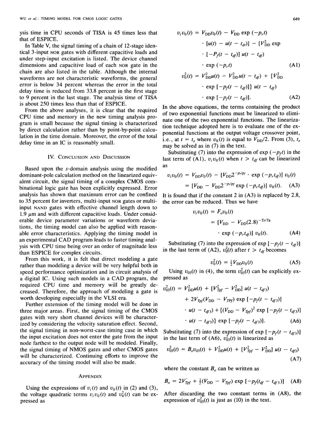
(0.9 Voo) /85/ $ IEEE. An Efficient Timing Model for CMOS Combinational Logic Gates
|
|
|
- Duane Morton
- 5 years ago
- Views:
Transcription
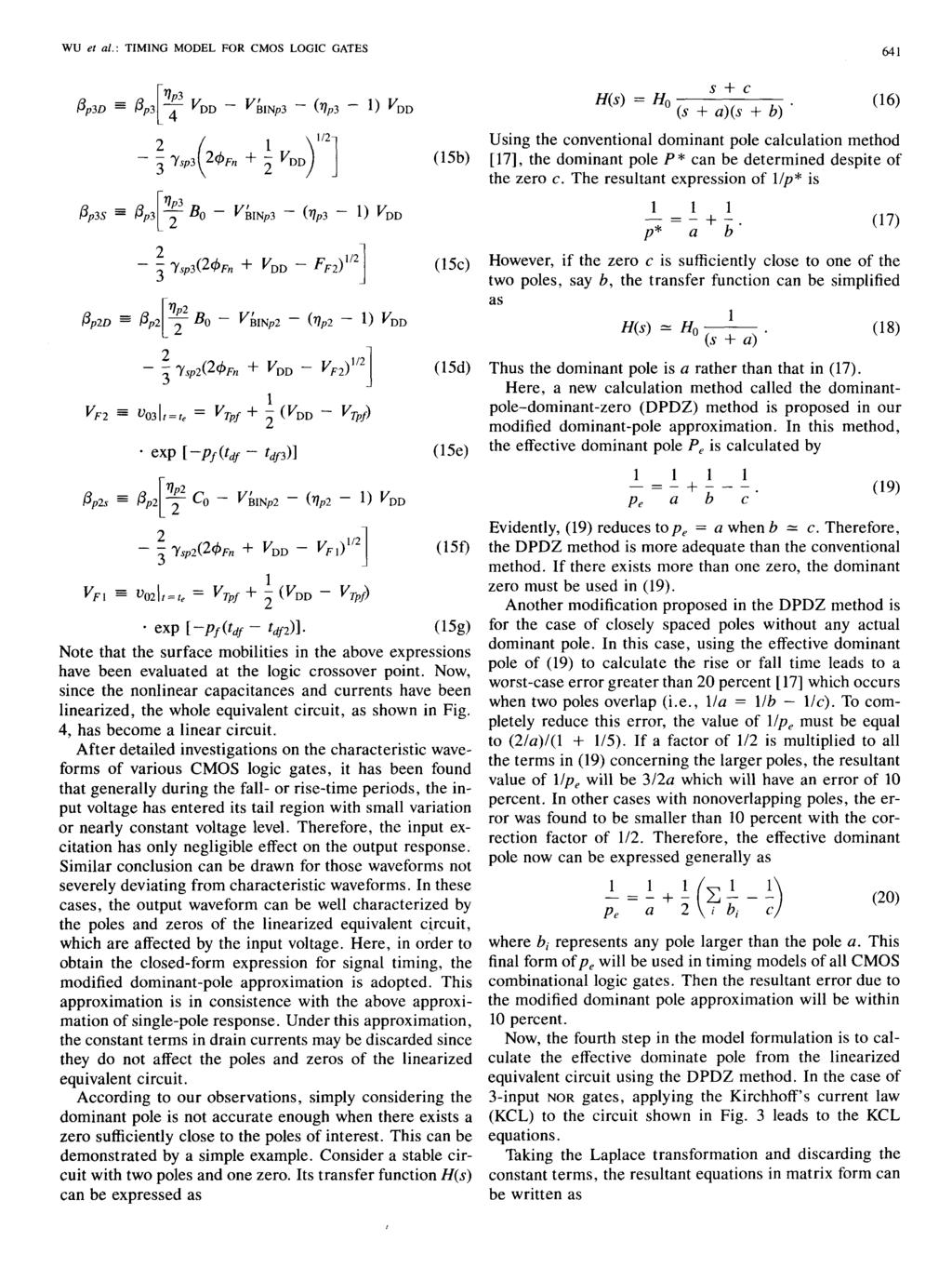
1 636 IEEE TRANSACTION S ON COMPUTER-AI D E D D E S IGN, VOL. CAO-4, NO.4, OCTOBER 1985 An Efficient Timing Model for CMOS Combinational Logic Gates CHUNG- YU WU, JEN-SHENG HWANG, CHIH CHANG, AND CHING-CHU CHANG Abstract-A new general timing model for CMOS combinational logic gates is proposed. In this model, the linearized large-signal equivalent circuit of a gate is first constructed. Then applying the dominant-poledominant-zero (DPDZ) method, the dominant pole of the equivalent circuit is calculated. Using this pole, the signal timing can be explicitly expressed. Comparisons between calculation results and simulation results are made and error analyses are performed. The worst-case error in characteristic-waveform timing can be confined to be within 35 percent for CMOS inverters, multi-input NOR gates or multi-input NAND gates with different device dimensions, capacitive loads, and device parameters. Better accuracy can be obtained for logic gates with commonly-used channel dimension or large capacitive load. For internal waveforms not deviating much from the characteristic waveforms, the worst-case uror in signal timing is not substantially increased. Applying the proposed timing model in an experimental timing simulator, the signal timing can be analyzed accurately and efficiently with reduced CPU time and memory. LIST OF SYMBOLS B Mobility correction parameter (SPICE device parameter). Cbdn(p) Bulk-drain p-n junction capacitance of an n-channel (p-channel) MOSFET. Cbsn( P ) Bulk-source p-n junction capacitance of an n-channel (p-channel) MOSFET. Cgdoun(p) Gate-drain overlap capacitance of an n channel (p-channel) MOSFET. Cgsoun(p) Gate-source overlap capacitance of an n channel (p-channel) MOSFET. CL Fixed load capacitance of a logic gate. Con(P) Channel oxide capacitance of an n-channel (p-channel) MOSFET. DELT A Channel width factor (SPICE device parameter). GAMMA Bulk threshold parameter in SPICE, which represents the proportionality factor relating the change in threshold voltage to backgate bias. Idn(p) Drain current of an n- channel (p-channel) MOSFET in large-signal model. Manuscript received October 8, 1984; revised January 8, This work was supported by ERSO, IT RI, Republic of China. C.-Y. Wu was with the Institute of Electronics, National Chiao-Tung University, Hsin-Chu, Taiwan, Republic of China. He is now with the Department of Electrical Engineering, School of Engineering and Applied Science, Portland State University, Portland, OR Y.-H. Yang is with the Institute of Electronics,-National Chiao-Tung University, Hsin-Chu, Taiwan, Republic of China. C. Chang and C.-C. Chang are with the Electronic Research and Service Organization. Industrial Technology Research Institute, Hsin-Chu, Taiwan, Republic of China. l o s DC drain current of an MOSFET. Leff Effective channel length of an MOSFET. NSUB Substrate Doping. Pier) Effective dominant pole in the fall (rise) characteristic waveform case. Dominant pole (zero) in the fall characteristic waveform case. Dominant pole (zero) in the rise characteristic waveform case. q Magnitude of electronic charge. Initial fall (rise) delay time. PId(Zfd) Prd(Zrd) tdi(r) T F(R) Fall (rise) time which is the time interval within which the output voltage lowers (raises) from 0.9 Voo (0.1 Voo) to 0.1 Voo (0.9 Voo). T ox Channel oxide thickness. Tp, Pair delay time which is the sum of fall del ay time and rise delay time. TpHL(LH) Fall (rise) del ay time which is the time interval between Vi = Voo to Va = Voo UCRIT Critical field for mobility degradation (SPICE device parameter). UEXP Critical field exponent in mobility degradation (SPICE device parameter). UEXPL (W) Correction factor of UEXP for short channel (narrow channel) case (SPICE device parameter). UO Surface mobility (SPICE device parameter). UOL(W) Correction factor of UO for short channel (narrow channel) case (SPICE device parameter). Vi(o) Input (output) large-signal voltage of a logic gate. V02(3) Large-signal voltage at internal nodes of a 3-input CMOS NOR gate. VBS(D) Bulk-source (drain) reverse bias of an MOSFET. Voo Power supply voltage. Drain (gate) source voltage of an MOS FET. Maximum drift velocity of carriers. Threshold voltage of an MOSFET under backgate bias. V TO Zero-bias threshold voltage of the MOS FET (SPICE device parameter). Weff Effective channel width of an MOSFET. VOS(GS) Vrnax VT /85/ $ IEEE
2
3
4
5
6
7
8
9
10
11
12
13
14
15
Timing macromodels for CMOS static setheset latches and their applications
 Timing macromodels for CMOS static setheset latches and their applications c.-y. wu C. Li J.S. Hwang Indexing terms: Modelling, Logic Abstract: Efficient timing macromodels for CMOS static NAND-type and
INTRODUCTION TO MOS TECHNOLOGY
 INTRODUCTION TO MOS TECHNOLOGY 1. The MOS transistor The most basic element in the design of a large scale integrated circuit is the transistor. For the processes we will discuss, the type of transistor
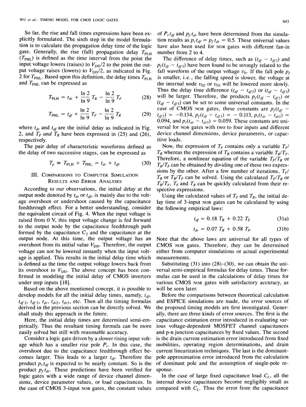
Field-Effect Transistor (FET) is one of the two major transistors; FET derives its name from its working mechanism;
 is one of the two major transistors; FET derives its name from its working mechanism;") Chapter 3 Field-Effect Transistors (FETs) 3.1 Introduction Field-Effect Transistor (FET) is one of the two major transistors; FET derives its name from its working mechanism; The concept has been known
Chapter 3 Field-Effect Transistors (FETs) 3.1 Introduction Field-Effect Transistor (FET) is one of the two major transistors; FET derives its name from its working mechanism; The concept has been known
Electronic CAD Practical work. Week 1: Introduction to transistor models. curve tracing of NMOS transfer characteristics
 Electronic CAD Practical work Dr. Martin John Burbidge Lancashire UK Tel: +44 (0)1524 825064 Email: martin@mjb-rfelectronics-synthesis.com Martin Burbidge 2006 Week 1: Introduction to transistor models
CMOS voltage controlled floating resistor
 INT. J. ELECTRONICS, 1996, VOL. 81, NO. 5, 571± 576 CMOS voltage controlled floating resistor HASSAN O. ELWAN², SOLIMAN A. MAHMOUD² AHMED M. SOLIMAN² and A new CMOS floating linear resistor circuit with
INTRODUCTION TO CIRCUIT SIMULATION USING SPICE
 LSI Circuits INTRODUCTION TO CIRCUIT SIMULATION USING SPICE Introduction: SPICE (Simulation Program with Integrated Circuit Emphasis) is a very powerful and probably the most widely used simulator for
PROCESS and environment parameter variations in scaled
 1078 IEEE TRANSACTIONS ON CIRCUITS AND SYSTEMS II: EXPRESS BRIEFS, VOL. 53, NO. 10, OCTOBER 2006 Reversed Temperature-Dependent Propagation Delay Characteristics in Nanometer CMOS Circuits Ranjith Kumar
LECTURE 4 SPICE MODELING OF MOSFETS
 LECTURE 4 SPICE MODELING OF MOSFETS Objectives for Lecture 4* Understanding the element description for MOSFETs Understand the meaning and significance of the various parameters in SPICE model levels 1
SPICE MODELING OF MOSFETS. Objectives for Lecture 4*
 LECTURE 4 SPICE MODELING OF MOSFETS Objectives for Lecture 4* Understanding the element description for MOSFETs Understand the meaning and significance of the various parameters in SPICE model levels 1
Lecture 16: MOS Transistor models: Linear models, SPICE models. Context. In the last lecture, we discussed the MOS transistor, and
 Lecture 16: MOS Transistor models: Linear models, SPICE models Context In the last lecture, we discussed the MOS transistor, and added a correction due to the changing depletion region, called the body
Modeling MOS Transistors. Prof. MacDonald
 Modeling MOS Transistors Prof. MacDonald 1 Modeling MOSFETs for simulation l Software is used simulate circuits for validation l Original program SPICE UC Berkeley Simulation Program with Integrated Circuit
Conduction Characteristics of MOS Transistors (for fixed Vds)! Topic 2. Basic MOS theory & SPICE simulation. MOS Transistor
! Topic 2. Basic MOS theory & SPICE simulation. MOS Transistor") Conduction Characteristics of MOS Transistors (for fixed Vds)! Topic 2 Basic MOS theory & SPICE simulation Peter Cheung Department of Electrical & Electronic Engineering Imperial College London (Weste&Harris,
Conduction Characteristics of MOS Transistors (for fixed Vds)! Topic 2 Basic MOS theory & SPICE simulation Peter Cheung Department of Electrical & Electronic Engineering Imperial College London (Weste&Harris,
Topic 2. Basic MOS theory & SPICE simulation
 Topic 2 Basic MOS theory & SPICE simulation Peter Cheung Department of Electrical & Electronic Engineering Imperial College London (Weste&Harris, Ch 2 & 5.1-5.3 Rabaey, Ch 3) URL: www.ee.ic.ac.uk/pcheung/
Conduction Characteristics of MOS Transistors (for fixed Vds) Topic 2. Basic MOS theory & SPICE simulation. MOS Transistor
 Topic 2. Basic MOS theory & SPICE simulation. MOS Transistor") Conduction Characteristics of MOS Transistors (for fixed Vds) Topic 2 Basic MOS theory & SPICE simulation Peter Cheung Department of Electrical & Electronic Engineering Imperial College London (Weste&Harris,
Conduction Characteristics of MOS Transistors (for fixed Vds) Topic 2 Basic MOS theory & SPICE simulation Peter Cheung Department of Electrical & Electronic Engineering Imperial College London (Weste&Harris,
FUNDAMENTALS OF MODERN VLSI DEVICES
 19-13- FUNDAMENTALS OF MODERN VLSI DEVICES YUAN TAUR TAK H. MING CAMBRIDGE UNIVERSITY PRESS Physical Constants and Unit Conversions List of Symbols Preface page xi xiii xxi 1 INTRODUCTION I 1.1 Evolution
Digital Electronics. By: FARHAD FARADJI, Ph.D. Assistant Professor, Electrical and Computer Engineering, K. N. Toosi University of Technology
 K. N. Toosi University of Technology Chapter 7. Field-Effect Transistors By: FARHAD FARADJI, Ph.D. Assistant Professor, Electrical and Computer Engineering, K. N. Toosi University of Technology http://wp.kntu.ac.ir/faradji/digitalelectronics.htm
ECE520 VLSI Design. Lecture 2: Basic MOS Physics. Payman Zarkesh-Ha
 ECE520 VLSI Design Lecture 2: Basic MOS Physics Payman Zarkesh-Ha Office: ECE Bldg. 230B Office hours: Wednesday 2:00-3:00PM or by appointment E-mail: pzarkesh@unm.edu Slide: 1 Review of Last Lecture Semiconductor
MOS Field Effect Transistors
 MOS Field Effect Transistors A gate contact gate interconnect n polysilicon gate source contacts W active area (thin oxide area) polysilicon gate contact metal interconnect drain contacts A bulk contact
Session 10: Solid State Physics MOSFET
 Session 10: Solid State Physics MOSFET 1 Outline A B C D E F G H I J 2 MOSCap MOSFET Metal-Oxide-Semiconductor Field-Effect Transistor: Al (metal) SiO2 (oxide) High k ~0.1 ~5 A SiO2 A n+ n+ p-type Si (bulk)
problem grade total
 Fall 2005 6.012 Microelectronic Devices and Circuits Prof. J. A. del Alamo Name: Recitation: November 16, 2005 Quiz #2 problem grade 1 2 3 4 total General guidelines (please read carefully before starting):
8. Combinational MOS Logic Circuits
 8. Combinational MOS Introduction Combinational logic circuits, or gates, witch perform Boolean operations on multiple input variables and determine the output as Boolean functions of the inputs, are the
Lecture-45. MOS Field-Effect-Transistors Threshold voltage
 Lecture-45 MOS Field-Effect-Transistors 7.4. Threshold voltage In this section we summarize the calculation of the threshold voltage and discuss the dependence of the threshold voltage on the bias applied
Depletion-mode operation ( 공핍형 ): Using an input gate voltage to effectively decrease the channel size of an FET
: Using an input gate voltage to effectively decrease the channel size of an FET") Ch. 13 MOSFET Metal-Oxide-Semiconductor Field-Effect Transistor : I D D-mode E-mode V g The gate oxide is made of dielectric SiO 2 with e = 3.9 Depletion-mode operation ( 공핍형 ): Using an input gate voltage
Ch. 13 MOSFET Metal-Oxide-Semiconductor Field-Effect Transistor : I D D-mode E-mode V g The gate oxide is made of dielectric SiO 2 with e = 3.9 Depletion-mode operation ( 공핍형 ): Using an input gate voltage
97.398*, Physical Electronics, Lecture 21. MOSFET Operation
 97.398*, Physical Electronics, Lecture 21 MOSFET Operation Lecture Outline Last lecture examined the MOSFET structure and required processing steps Now move on to basic MOSFET operation, some of which
MOS TRANSISTOR THEORY
 MOS TRANSISTOR THEORY Introduction A MOS transistor is a majority-carrier device, in which the current in a conducting channel between the source and the drain is modulated by a voltage applied to the
Power MOSFET Zheng Yang (ERF 3017,
 ECE442 Power Semiconductor Devices and Integrated Circuits Power MOSFET Zheng Yang (ERF 3017, email: yangzhen@uic.edu) Evolution of low-voltage (
55:041 Electronic Circuits
 55:041 Electronic Circuits MOSFETs Sections of Chapter 3 &4 A. Kruger MOSFETs, Page-1 Basic Structure of MOS Capacitor Sect. 3.1 Width = 1 10-6 m or less Thickness = 50 10-9 m or less ` MOS Metal-Oxide-Semiconductor
Lecture 4. MOS transistor theory
 Lecture 4 MOS transistor theory 1.7 Introduction: A MOS transistor is a majority-carrier device, in which the current in a conducting channel between the source and the drain is modulated by a voltage
Lecture 24 - The Si surface and the Metal-Oxide-Semiconductor Structure (cont.) The Long Metal-Oxide-Semiconductor Field-Effect Transistor
 The Long Metal-Oxide-Semiconductor Field-Effect Transistor") 6.720J/3.43J - Integrated Microelectronic Devices - Spring 2007 Lecture 24-1 Lecture 24 - The Si surface and the Metal-Oxide-Semiconductor Structure (cont.) The Long Metal-Oxide-Semiconductor Field-Effect
6.720J/3.43J - Integrated Microelectronic Devices - Spring 2007 Lecture 24-1 Lecture 24 - The Si surface and the Metal-Oxide-Semiconductor Structure (cont.) The Long Metal-Oxide-Semiconductor Field-Effect
ECE/CoE 0132: FETs and Gates
 ECE/CoE 0132: FETs and Gates Kartik Mohanram September 6, 2017 1 Physical properties of gates Over the next 2 lectures, we will discuss some of the physical characteristics of integrated circuits. We will
NAME: Last First Signature
 UNIVERSITY OF CALIFORNIA, BERKELEY College of Engineering Department of Electrical Engineering and Computer Sciences EE 130: IC Devices Spring 2003 FINAL EXAMINATION NAME: Last First Signature STUDENT
MEASUREMENT AND INSTRUMENTATION STUDY NOTES UNIT-I
 MEASUREMENT AND INSTRUMENTATION STUDY NOTES The MOSFET The MOSFET Metal Oxide FET UNIT-I As well as the Junction Field Effect Transistor (JFET), there is another type of Field Effect Transistor available
UNIT-1 Bipolar Junction Transistors. Text Book:, Microelectronic Circuits 6 ed., by Sedra and Smith, Oxford Press
 UNIT-1 Bipolar Junction Transistors Text Book:, Microelectronic Circuits 6 ed., by Sedra and Smith, Oxford Press Figure 6.1 A simplified structure of the npn transistor. Microelectronic Circuits, Sixth
Difference between BJTs and FETs. Junction Field Effect Transistors (JFET)
") Difference between BJTs and FETs Transistors can be categorized according to their structure, and two of the more commonly known transistor structures, are the BJT and FET. The comparison between BJTs
Difference between BJTs and FETs Transistors can be categorized according to their structure, and two of the more commonly known transistor structures, are the BJT and FET. The comparison between BJTs
EE 42/100 Lecture 23: CMOS Transistors and Logic Gates. Rev A 4/15/2012 (10:39 AM) Prof. Ali M. Niknejad
 Prof. Ali M. Niknejad") A. M. Niknejad University of California, Berkeley EE 100 / 42 Lecture 23 p. 1/16 EE 42/100 Lecture 23: CMOS Transistors and Logic Gates ELECTRONICS Rev A 4/15/2012 (10:39 AM) Prof. Ali M. Niknejad University
A. M. Niknejad University of California, Berkeley EE 100 / 42 Lecture 23 p. 1/16 EE 42/100 Lecture 23: CMOS Transistors and Logic Gates ELECTRONICS Rev A 4/15/2012 (10:39 AM) Prof. Ali M. Niknejad University
AS THE semiconductor process is scaled down, the thickness
 IEEE TRANSACTIONS ON CIRCUITS AND SYSTEMS II: EXPRESS BRIEFS, VOL. 52, NO. 7, JULY 2005 361 A New Schmitt Trigger Circuit in a 0.13-m 1/2.5-V CMOS Process to Receive 3.3-V Input Signals Shih-Lun Chen,
Digital Electronics Part II - Circuits
 Digital Electronics Part II - Circuits Dr. I. J. Wassell Gates from Transistors 1 Introduction Logic circuits are non-linear, consequently we will introduce a graphical technique for analysing such circuits
EE105 Fall 2015 Microelectronic Devices and Circuits: MOSFET Prof. Ming C. Wu 511 Sutardja Dai Hall (SDH)
") EE105 Fall 2015 Microelectronic Devices and Circuits: MOSFET Prof. Ming C. Wu wu@eecs.berkeley.edu 511 Sutardja Dai Hall (SDH) 7-1 Simplest Model of MOSFET (from EE16B) 7-2 CMOS Inverter 7-3 CMOS NAND
EE105 Fall 2015 Microelectronic Devices and Circuits: MOSFET Prof. Ming C. Wu wu@eecs.berkeley.edu 511 Sutardja Dai Hall (SDH) 7-1 Simplest Model of MOSFET (from EE16B) 7-2 CMOS Inverter 7-3 CMOS NAND
Low Power Realization of Subthreshold Digital Logic Circuits using Body Bias Technique
 Indian Journal of Science and Technology, Vol 9(5), DOI: 1017485/ijst/2016/v9i5/87178, Februaru 2016 ISSN (Print) : 0974-6846 ISSN (Online) : 0974-5645 Low Power Realization of Subthreshold Digital Logic
ECE 340 Lecture 40 : MOSFET I
 ECE 340 Lecture 40 : MOSFET I Class Outline: MOS Capacitance-Voltage Analysis MOSFET - Output Characteristics MOSFET - Transfer Characteristics Things you should know when you leave Key Questions How do
INTERNATIONAL JOURNAL OF APPLIED ENGINEERING RESEARCH, DINDIGUL Volume 1, No 3, 2010
 Low Power CMOS Inverter design at different Technologies Vijay Kumar Sharma 1, Surender Soni 2 1 Department of Electronics & Communication, College of Engineering, Teerthanker Mahaveer University, Moradabad
UNIT-1 Fundamentals of Low Power VLSI Design
 UNIT-1 Fundamentals of Low Power VLSI Design Need for Low Power Circuit Design: The increasing prominence of portable systems and the need to limit power consumption (and hence, heat dissipation) in very-high
3084 IEEE TRANSACTIONS ON NUCLEAR SCIENCE, VOL. 60, NO. 4, AUGUST 2013
 3084 IEEE TRANSACTIONS ON NUCLEAR SCIENCE, VOL. 60, NO. 4, AUGUST 2013 Dummy Gate-Assisted n-mosfet Layout for a Radiation-Tolerant Integrated Circuit Min Su Lee and Hee Chul Lee Abstract A dummy gate-assisted
Semiconductor Physics and Devices
 Metal-Semiconductor and Semiconductor Heterojunctions The Metal-Oxide-Semiconductor Field-Effect Transistor (MOSFET) is one of two major types of transistors. The MOSFET is used in digital circuit, because
Atomic-layer deposition of ultrathin gate dielectrics and Si new functional devices
 Atomic-layer deposition of ultrathin gate dielectrics and Si new functional devices Anri Nakajima Research Center for Nanodevices and Systems, Hiroshima University 1-4-2 Kagamiyama, Higashi-Hiroshima,
Final for EE 421 Digital Electronics and ECG 621 Digital Integrated Circuit Design Fall, University of Nevada, Las Vegas
 Final for EE 421 Digital Electronics and ECG 621 Digital Integrated Circuit Design Fall, University of Nevada, Las Vegas NAME: Show your work to get credit. Open book and closed notes. Unless otherwise
ECE4902 B2015 HW Set 1
 ECE4902 B2015 HW Set 1 Due in class Tuesday November 3. To make life easier on the graders: Be sure your NAME and ECE MAILBOX NUMBER are prominently displayed on the upper right of what you hand in. When
Field Effect Transistors
 Field Effect Transistors LECTURE NO. - 41 Field Effect Transistors www.mycsvtunotes.in JFET MOSFET CMOS Field Effect transistors - FETs First, why are we using still another transistor? BJTs had a small
ECE 334: Electronic Circuits Lecture 10: Digital CMOS Circuits
 Faculty of Engineering ECE 334: Electronic Circuits Lecture 10: Digital CMOS Circuits CMOS Technology Complementary MOS, or CMOS, needs both PMOS and NMOS FET devices for their logic gates to be realized
ECE380 Digital Logic. Logic values as voltage levels
 ECE380 Digital Logic Implementation Technology: NMOS and PMOS Transistors, CMOS logic gates Dr. D. J. Jackson Lecture 13-1 Logic values as voltage levels V ss is the minimum voltage that can exist in the
Education on CMOS RF Circuit Reliability
 Education on CMOS RF Circuit Reliability Jiann S. Yuan 1 Abstract This paper presents a design methodology to study RF circuit performance degradations due to hot carrier and soft breakdown. The experimental
Leakage Current Modeling in PD SOI Circuits
 Leakage Current Modeling in PD SOI Circuits Mini Nanua David Blaauw Chanhee Oh Sun MicroSystems University of Michigan Nascentric Inc. mini.nanua@sun.com blaauw@umich.edu chanhee.oh@nascentric.com Abstract
Temperature-adaptive voltage tuning for enhanced energy efficiency in ultra-low-voltage circuits
 Microelectronics Journal 39 (2008) 1714 1727 www.elsevier.com/locate/mejo Temperature-adaptive voltage tuning for enhanced energy efficiency in ultra-low-voltage circuits Ranjith Kumar, Volkan Kursun Department
MOSFET short channel effects
 MOSFET short channel effects overview Five different short channel effects can be distinguished: velocity saturation drain induced barrier lowering (DIBL) impact ionization surface scattering hot electrons
SUBTHRESHOLD CIRCUIT DESIGN FOR HIGH PERFORMANCE
 SUBTHRESHOLD CIRCUIT DESIGN FOR HIGH PERFORMANCE K. VIKRANTH REDDY 1, M. MURALI KRISHNA 2, K. LAL KISHORE 3 1 M.Tech. Student, Department of ECE, GITAM University, Visakhapatnam, INDIA 2 Assistant Professor,
8. Characteristics of Field Effect Transistor (MOSFET)
") 1 8. Characteristics of Field Effect Transistor (MOSFET) 8.1. Objectives The purpose of this experiment is to measure input and output characteristics of n-channel and p- channel field effect transistors
1 8. Characteristics of Field Effect Transistor (MOSFET) 8.1. Objectives The purpose of this experiment is to measure input and output characteristics of n-channel and p- channel field effect transistors
EE301 Electronics I , Fall
 EE301 Electronics I 2018-2019, Fall 1. Introduction to Microelectronics (1 Week/3 Hrs.) Introduction, Historical Background, Basic Consepts 2. Rewiev of Semiconductors (1 Week/3 Hrs.) Semiconductor materials
Stacked-FET linear SOI CMOS SPDT antenna switch with input P1dB greater than
 LETTER IEICE Electronics Express, Vol.9, No.24, 1813 1822 Stacked-FET linear SOI CMOS SPDT antenna switch with input P1dB greater than 40 dbm Donggu Im 1a) and Kwyro Lee 1,2 1 Department of EE, Korea Advanced
ELEC 350L Electronics I Laboratory Fall 2012
 ELEC 350L Electronics I Laboratory Fall 2012 Lab #9: NMOS and CMOS Inverter Circuits Introduction The inverter, or NOT gate, is the fundamental building block of most digital devices. The circuits used
C H A P T E R 5. Amplifier Design
 C H A P T E 5 Amplifier Design The Common-Source Amplifier v 0 = r ( g mvgs )( D 0 ) A v0 = g m r ( D 0 ) Performing the analysis directly on the circuit diagram with the MOSFET model used implicitly.
Advanced Power MOSFET Concepts
 В. Jayant Baliga Advanced Power MOSFET Concepts Springer Contents 1 Introduction 1 1.1 Ideal Power Switching Waveforms 2 1.2 Ideal and Typical Power MOSFET Characteristics 3 1.3 Typical Power MOSFET Structures
Pramoda N V Department of Electronics and Communication Engineering, MCE Hassan Karnataka India
 Advanced Low Power CMOS Design to Reduce Power Consumption in CMOS Circuit for VLSI Design Pramoda N V Department of Electronics and Communication Engineering, MCE Hassan Karnataka India Abstract: Low
Fundamentos de Electrónica Lab Guide
 Fundamentos de Electrónica Lab Guide Field Effect Transistor MOS-FET IST-2016/2017 2 nd Semester I-Introduction These are the objectives: a. n-type MOSFET characterization from the I(U) characteristics.
Implementation of Full Adder using Cmos Logic
 ISSN: 232-9653; IC Value: 45.98; SJ Impact Factor:6.887 Volume 5 Issue VIII, July 27- Available at www.ijraset.com Implementation of Full Adder using Cmos Logic Ravika Gupta Undergraduate Student, Dept
ENEE307 Lab 7 MOS Transistors 2: Small Signal Amplifiers and Digital Circuits
 ENEE307 Lab 7 MOS Transistors 2: Small Signal Amplifiers and Digital Circuits In this lab, we will be looking at ac signals with MOSFET circuits and digital electronics. The experiments will be performed
55:041 Electronic Circuits
 55:041 Electronic Circuits Mosfet Review Sections of Chapter 3 &4 A. Kruger Mosfet Review, Page-1 Basic Structure of MOS Capacitor Sect. 3.1 Width 1 10-6 m or less Thickness 50 10-9 m or less ` MOS Metal-Oxide-Semiconductor
ESD-Transient Detection Circuit with Equivalent Capacitance-Coupling Detection Mechanism and High Efficiency of Layout Area in a 65nm CMOS Technology
 ESD-Transient Detection Circuit with Equivalent Capacitance-Coupling Detection Mechanism and High Efficiency of Layout Area in a 65nm CMOS Technology Chih-Ting Yeh (1, 2) and Ming-Dou Ker (1, 3) (1) Department
SUBTHRESHOLD operation of a MOSFET has long been
 IEEE TRANSACTIONS ON COMPUTER-AIDED DESIGN OF INTEGRATED CIRCUITS AND SYSTEMS, VOL. 16, NO. 4, APRIL 1997 343 A Three-Parameters-Only MOSFET Subthreshold Current CAD Model Considering Back-Gate Bias and
LECTURE 09 LARGE SIGNAL MOSFET MODEL
 Lecture 9 Large Signal MOSFET Model (5/14/18) Page 9-1 LECTURE 9 LARGE SIGNAL MOSFET MODEL LECTURE ORGANIZATION Outline Introduction to modeling Operation of the MOS transistor Simple large signal model
MOSFET Terminals. The voltage applied to the GATE terminal determines whether current can flow between the SOURCE & DRAIN terminals.
 MOSFET Terminals The voltage applied to the GATE terminal determines whether current can flow between the SOURCE & DRAIN terminals. For an n-channel MOSFET, the SOURCE is biased at a lower potential (often
Three Terminal Devices
 Three Terminal Devices - field effect transistor (FET) - bipolar junction transistor (BJT) - foundation on which modern electronics is built - active devices - devices described completely by considering
EFFECT OF THRESHOLD VOLTAGE AND CHANNEL LENGTH ON DRAIN CURRENT OF SILICON N-MOSFET
 EFFECT OF THRESHOLD VOLTAGE AND CHANNEL LENGTH ON DRAIN CURRENT OF SILICON N-MOSFET A.S.M. Bakibillah Nazibur Rahman Dept. of Electrical & Electronic Engineering, American International University Bangladesh
Solid State Device Fundamentals
 Solid State Device Fundamentals 4.4. Field Effect Transistor (MOSFET) ENS 463 Lecture Course by Alexander M. Zaitsev alexander.zaitsev@csi.cuny.edu Tel: 718 982 2812 4N101b 1 Field-effect transistor (FET)
Design of a High Speed Mixed Signal CMOS Mutliplying Circuit
 Brigham Young University BYU ScholarsArchive All Theses and Dissertations 2004-03-12 Design of a High Speed Mixed Signal CMOS Mutliplying Circuit David Ray Bartholomew Brigham Young University - Provo
Very Low Voltage Testing of SOI Integrated Circuits
 Very Low Voltage Testing of SOI Integrated Circuits Eric MacDonald Nur A.Touba IBM Microelectronics Division Computer Engineering Research Center 114 Burnet Road Dept. of Electrical and Computer Engineering
45nm Bulk CMOS Within-Die Variations. Courtesy of C. Spanos (UC Berkeley) Lecture 11. Process-induced Variability I: Random
 Lecture 11. Process-induced Variability I: Random") 45nm Bulk CMOS Within-Die Variations. Courtesy of C. Spanos (UC Berkeley) Lecture 11 Process-induced Variability I: Random Random Variability Sources and Characterization Comparisons of Different MOSFET
45nm Bulk CMOS Within-Die Variations. Courtesy of C. Spanos (UC Berkeley) Lecture 11 Process-induced Variability I: Random Random Variability Sources and Characterization Comparisons of Different MOSFET
Sub-Threshold Region Behavior of Long Channel MOSFET
 Sub-threshold Region - So far, we have discussed the MOSFET behavior in linear region and saturation region - Sub-threshold region is refer to region where Vt is less than Vt - Sub-threshold region reflects
International Journal of Scientific & Engineering Research, Volume 6, Issue 2, February-2015 ISSN
 Performance Evaluation and Comparison of Ultra-thin Bulk (UTB), Partially Depleted and Fully Depleted SOI MOSFET using Silvaco TCAD Tool Seema Verma1, Pooja Srivastava2, Juhi Dave3, Mukta Jain4, Priya
Exam Below are two schematics of current sources implemented with MOSFETs. Which current source has the best compliance voltage?
 Exam 2 Name: Score /90 Question 1 Short Takes 1 point each unless noted otherwise. 1. Below are two schematics of current sources implemented with MOSFETs. Which current source has the best compliance
Performance Comparison of CMOS and Finfet Based Circuits At 45nm Technology Using SPICE
 RESEARCH ARTICLE OPEN ACCESS Performance Comparison of CMOS and Finfet Based Circuits At 45nm Technology Using SPICE Mugdha Sathe*, Dr. Nisha Sarwade** *(Department of Electrical Engineering, VJTI, Mumbai-19)
NOVEL OSCILLATORS IN SUBTHRESHOLD REGIME
 NOVEL OSCILLATORS IN SUBTHRESHOLD REGIME Neeta Pandey 1, Kirti Gupta 2, Rajeshwari Pandey 3, Rishi Pandey 4, Tanvi Mittal 5 1, 2,3,4,5 Department of Electronics and Communication Engineering, Delhi Technological
Index. Small-Signal Models, 14 saturation current, 3, 5 Transistor Cutoff Frequency, 18 transconductance, 16, 22 transit time, 10
 Index A absolute value, 308 additional pole, 271 analog multiplier, 190 B BiCMOS,107 Bode plot, 266 base-emitter voltage, 16, 50 base-emitter voltages, 296 bias current, 111, 124, 133, 137, 166, 185 bipolar
(Refer Slide Time: 02:05)
") Electronics for Analog Signal Processing - I Prof. K. Radhakrishna Rao Department of Electrical Engineering Indian Institute of Technology Madras Lecture 27 Construction of a MOSFET (Refer Slide Time:
Electronics for Analog Signal Processing - I Prof. K. Radhakrishna Rao Department of Electrical Engineering Indian Institute of Technology Madras Lecture 27 Construction of a MOSFET (Refer Slide Time:
ECE 340 Lecture 37 : Metal- Insulator-Semiconductor FET Class Outline:
 ECE 340 Lecture 37 : Metal- Insulator-Semiconductor FET Class Outline: Metal-Semiconductor Junctions MOSFET Basic Operation MOS Capacitor Things you should know when you leave Key Questions What is the
Gechstudentszone.wordpress.com
 UNIT 4: Small Signal Analysis of Amplifiers 4.1 Basic FET Amplifiers In the last chapter, we described the operation of the FET, in particular the MOSFET, and analyzed and designed the dc response of circuits
MOSFET & IC Basics - GATE Problems (Part - I)
") MOSFET & IC Basics - GATE Problems (Part - I) 1. Channel current is reduced on application of a more positive voltage to the GATE of the depletion mode n channel MOSFET. (True/False) [GATE 1994: 1 Mark]
MOSFET & IC Basics - GATE Problems (Part - I) 1. Channel current is reduced on application of a more positive voltage to the GATE of the depletion mode n channel MOSFET. (True/False) [GATE 1994: 1 Mark]
Q1. Explain the construction and principle of operation of N-Channel and P-Channel Junction Field Effect Transistor (JFET).
.") Q. Explain the construction and principle of operation of N-Channel and P-Channel Junction Field Effect Transistor (JFET). Answer: N-Channel Junction Field Effect Transistor (JFET) Construction: Drain(D)
Q. Explain the construction and principle of operation of N-Channel and P-Channel Junction Field Effect Transistor (JFET). Answer: N-Channel Junction Field Effect Transistor (JFET) Construction: Drain(D)
Alternative Channel Materials for MOSFET Scaling Below 10nm
 Alternative Channel Materials for MOSFET Scaling Below 10nm Doug Barlage Electrical Requirements of Channel Mark Johnson Challenges With Material Synthesis Introduction Outline Challenges with scaling
Design cycle for MEMS
 Design cycle for MEMS Design cycle for ICs IC Process Selection nmos CMOS BiCMOS ECL for logic for I/O and driver circuit for critical high speed parts of the system The Real Estate of a Wafer MOS Transistor
A New Model for Thermal Channel Noise of Deep-Submicron MOSFETS and its Application in RF-CMOS Design
 IEEE JOURNAL OF SOLID-STATE CIRCUITS, VOL. 36, NO. 5, MAY 2001 831 A New Model for Thermal Channel Noise of Deep-Submicron MOSFETS and its Application in RF-CMOS Design Gerhard Knoblinger, Member, IEEE,
AS THE GATE-oxide thickness is scaled and the gate
 1174 IEEE TRANSACTIONS ON ELECTRON DEVICES, VOL. 46, NO. 6, JUNE 1999 A New Quasi-2-D Model for Hot-Carrier Band-to-Band Tunneling Current Kuo-Feng You, Student Member, IEEE, and Ching-Yuan Wu, Member,
Lecture 16. Complementary metal oxide semiconductor (CMOS) CMOS 1-1
 CMOS 1-1") Lecture 16 Complementary metal oxide semiconductor (CMOS) CMOS 1-1 Outline Complementary metal oxide semiconductor (CMOS) Inverting circuit Properties Operating points Propagation delay Power dissipation
Lecture 16 Complementary metal oxide semiconductor (CMOS) CMOS 1-1 Outline Complementary metal oxide semiconductor (CMOS) Inverting circuit Properties Operating points Propagation delay Power dissipation
BJT Amplifier. Superposition principle (linear amplifier)
") BJT Amplifier Two types analysis DC analysis Applied DC voltage source AC analysis Time varying signal source Superposition principle (linear amplifier) The response of a linear amplifier circuit excited
BJT Amplifier Two types analysis DC analysis Applied DC voltage source AC analysis Time varying signal source Superposition principle (linear amplifier) The response of a linear amplifier circuit excited
Intro to Electricity. Introduction to Transistors. Example Circuit Diagrams. Water Analogy
 Introduction to Transistors Transistors form the basic building blocks of all computer hardware. Invented by William Shockley, John Bardeen and Walter Brattain in 1947, replacing previous vaccuumtube technology
UNIT 3: FIELD EFFECT TRANSISTORS
 FIELD EFFECT TRANSISTOR: UNIT 3: FIELD EFFECT TRANSISTORS The field effect transistor is a semiconductor device, which depends for its operation on the control of current by an electric field. There are
Computer Exercises Manual: Device Parameters in SPICE. Interactive MATLAB Animations for Understanding Semiconductor Devices
 Computer Exercises Manual: Device Parameters in SPICE This manual is provided as a PDF le { just click on cem.pdf to open it. This can be done from the CD (using Windows Explorer, click on the CD-drive
CHAPTER 6 DIGITAL CIRCUIT DESIGN USING SINGLE ELECTRON TRANSISTOR LOGIC
 94 CHAPTER 6 DIGITAL CIRCUIT DESIGN USING SINGLE ELECTRON TRANSISTOR LOGIC 6.1 INTRODUCTION The semiconductor digital circuits began with the Resistor Diode Logic (RDL) which was smaller in size, faster
Week 7: Common-Collector Amplifier, MOS Field Effect Transistor
 EE 2110A Electronic Circuits Week 7: Common-Collector Amplifier, MOS Field Effect Transistor ecture 07-1 Topics to coer Common-Collector Amplifier MOS Field Effect Transistor Physical Operation and I-V
DG-FINFET LOGIC DESIGN USING 32NM TECHNOLOGY
 International Journal of Knowledge Management & e-learning Volume 3 Number 1 January-June 2011 pp. 1-5 DG-FINFET LOGIC DESIGN USING 32NM TECHNOLOGY K. Nagarjuna Reddy 1, K. V. Ramanaiah 2 & K. Sudheer
Performance Analysis of Energy Efficient and Charge Recovery Adiabatic Techniques for Low Power Design
 IOSR Journal of Engineering (IOSRJEN) e-issn: 2250-3021, p-issn: 2278-8719 Vol. 3, Issue 6 (June. 2013), V1 PP 14-21 Performance Analysis of Energy Efficient and Charge Recovery Adiabatic Techniques for