EUVL Exposure Tools for HVM: It s Under (and About) Control
|
|
|
- Samantha Walker
- 6 years ago
- Views:
Transcription

1 EUVL Exposure Tools for HVM: It s Under (and About) Control Wim van der Zande ASML Director, Research EUV Litho Workshop Amsterdam November 2016
2 ASML at a EUV Source Workshop Slide 2 The position of EUV for continuation of advanced lithography solutions: More than simply shrink EUV Installed base performance: Imaging, overlay, defectivity: status and implication EUV source architecture, performance and power scaling: The beauty of the ASML EUV Source Summary
3 Acknowledgements: Igor Fomenkov, David Brandt, Daniel Brown, Rob Rafac, Alexander Schafgans, Yezheng Tao, Michael Purvis, Alex Ershov, Georgiy Vaschenko, Slava Rokitski, Michael Kats, Daniel Riggs, Wayne Dunstan, Michael Varga, Mathew Abraham, Matthew Graham, Slide 3 Cymer LLC, Thornmint Ct, San Diego, CA USA Marco Pieters, Rudy Peeters, Daniel Smith, Uwe Stamm, Sjoerd Lok, Arthur Minnaert, Martijn van Noordenburg, Joerg Mallmann, David Ockwell, Henk Meijer, Judon Stoeldraijer, Christian Wagner, Carmen Zoldesi, Eelco van Setten, Jo Finders, Koen de Peuter, Chris de Ruijter, Milos Popadic, Roger Huang, Roderik van Es, Marcel Beckers, Hans Meiling,..... ASML Netherlands B.V., De Run 6501, 5504 DR Veldhoven, The Netherlands
4 Minimum Resolution, Half Pitch [nm] Shrink drives need for advanced lithography solutions Minimum Resolution of Critical Device Features 70nm 50nm MPU Metal interconnect 3D NAND Memory Pipe xx Minimum resolution Effective 3D resolution Number of 3D or x-point stacks Confidential Slide 4 11/17/ nm 20nm 10nm 8nm 2D NAND Bit & Word Line 24 3D NAND Half pitch / # stacks 32 Foundry Metal interconnect DRAM Bit line X-point Bit & Word Lines 6nm nm 3nm X-point Half pitch / # stacks Year Production Start
5 Overlay [nm] Focus [nm] Requirements for Overlay & Focus are challenging Year HVM Logic - Foundry 20 nm nm 10 nm 7 nm 5 nm Slide 5 June 22, 2016 Logic - MPU DRAM NAND planar & 3D X-Point 22 nm 14 nm 10 nm 7 nm D2xM D2xL D1xH D1xM D1x 19 nm 3D x24 3D x32 16 nm 3D x48 14 nm 3D x64 3D x96 3D x128 x192 2x x2 2x x4 1x x4 1x x8 Production Ramp R&D Roadmap On-Product Overlay ~ 4.0 nm 5.0 ~ 3.5 nm 5.0 ~ 3.5 nm 4.5 ~ 2.5 nm 3.5 ~ 2.5 nm 2.5 ~ 2.0 nm 2.5 ~ 1.8 nm On-Product Focus 2 90 ~ 60 nm 80 ~ 60 nm 70 ~ 60 nm 60 ~ 50 nm 60 ~ 50 nm 50 ~ 40 nm 50 ~ 40 nm 1 Range for Logic & Memory critical layers 2 Range for EUV & ArF immersion foundry production wafer focus control requirements with process window enhancement techniques Holistic Overlay Roadmap On Product Overlay Matched Scanner Overlay Application & Process Holistic Immersion Focus Control Roadmap On Product Focus Control Scanner Focus Control Application & Process


6 ASML s holistic shrink roadmap: DUV-EUV coexistence Slide 6 Extend DUV to support multiple patterning Introduce EUV to volume manufacturing Support both with a suite of process window enhancement, control and calibration products
7 Slide 7 12 Jan 2016 EUV Why It Helps


8 EUV single exposure replaces immersion multiple patterning 2D-Metal at 32nm pitch achieved with Quasar illumination Confidential Slide 8 April 2016 ArFi LE 3 (triple patterning) EUV Single Exposure 32nm pitch / 16nm CD Dose: 20 mj/cm 2 48nm pitch / 24nm CD Quasar Quasar, illumination Pupil Pupil Fill ratio Fill 20% ratio 20% In cooperation with IMEC


9 EUV: The overall economic value to Customers Slide Per-layer patterning cost comparison EUV clear winner for critical layers (3x ArFi immersion and above) Shorter cycles of learning = faster time to market Single-expose layers reduce process complexity (6-month gain) 3 Steeper ramp to higher yield Fewer multiple patterning layers mean higher yield (up to 9%) 4 Superior electrical properties Better binning 5 In a full fab, EUV enables higher output DRAM example: 78% vs 62% bit growth
10 Increasing Yield 2 Faster yield ramp with EUV means faster time to market Slide 10 6 months 1D-ArFi 1D-EUV 2D-EUV May June July Aug Sept Oct Nov Dec Jan Feb Mar Apr May June A simpler process goes through yield ramp faster


11 4 Electrical data confirms: EUV enables superior devices Slide 11 SADP: Self aligned double patterning
12 Slide Jan 2016 EUV Where are we now
13 Customer Confidence in EUV continues to increase Slide 13 Source power 125W configuration at customer sites 210 Watts of dose-controlled EUV power demonstrated Availability Five customer systems have achieved a four-week average availability of more than 80%; however, consistency still needs to be improved Productivity More than 1,200 wafers per day (wpd) exposed on NXE:3350B at a customer site Peak performance near target of 1500 wpd (achieved 1488 wpd at ASML)
14 NXE extension roadmap to optimize capital efficiency Slide 14 1 st system shipment 2013 Logic DRAM 55 WPH 125 WPH 145 WPH 185 WPH R&D NXE:3300B 250W LPP Half pitch 22 nm Focus* 110 nm DCO/MMO 3.0/5.0 nm OPO * 7.0 nm UVLS D1H SNEP 3350B NXE:3350B 16 nm 70 nm 1.5/2.5 nm 3.5 nm D1M 20% PFR illuminator OFP 3350B-3400B NXE:3400B 350W LPP 13 nm 60 nm 1.4/<2.0 nm 2.5 nm x D1L UVLS Mk2 Orion 200 Lens thermal NXE:3450C 13 nm 50 nm 1.2/<1.7 nm 2.0 nm <D1L ~2.5 Products under study 500W source Anamorphic lens Stages, handlers High NA <8 nm <40 nm 1.0/<1.4 nm 1.5 nm Roadmap: July 2016 * On product overlay (OPO) and focus are not ATP specs, but required performance for specific customer nodes to be achieved including Application and DUV configuration
15 Slide Jan 2016 EUV Installed Base

16 NXE:3350B: 2x overlay improvement at 16nm resolution Supporting 7nm logic, ~15nm DRAM requirements Slide 16 Overlay set up Set-up and modeling improvements Reticle Stage Better thermal control increased servo bandwidth Projection Optics Higher lens transmission improved aberrations and distortion SMASH sensor Improved alignment sensor Off-Axis Illuminator FlexPupil Wafer Stage Improved thermal control Resolution Full wafer CDU DCO MMO 16nm < 1.3nm < 1.5nm < 2.5nm Spotless NXE Automated wafer table cleaning Focus control < 70nm Productivity 125 WPH New UV level sensor Improved air mounts Overlay Imaging/Focus Productivity
17 Total number of wafers exposed >405k wafers exposed on NXE:3300B at customer sites Currently 8 systems running in the field Slide , , , , , , , ,000 50, Week

18 NXE:3350B: 125W settings qualified Slide 18 Mean pulse energy at Intermediate Focus ~3mJ EUV power at Intermediate Focus 125W Energy control Overhead ~20%
 3100 MOPA (not")

19 Dose controlled EUV power (W) Progress in source power supporting productivity roadmap to >125 WPH Slide NOMO (delivered) 3100 MOPA (not shipped) 3100 MOPA+PP (not shipped) 3300 MOPA+PP (delivered) 3400 MOPA+PP (development) Year CE~5.5% 210W with dose in specifications obtained on development source
20 Slide Jan 2016 EUV Installed Base: more than power alone


 SEM image @BE/BF Dose 40 mj/cm 2 25 mj/cm 2")


21 Process: resist towards 16nm resolution at 125 WPH 19% EL, 4.4nm 2. Also 13nm resolved with 17% EL and 4.2nm 2 Slide 21 NXE:3350B 16nm Horizontal Dense lines/spaces 13nm Horizontal Dense lines/spaces Reference CAR New formulation CAR New Inpria resist (NTI non-car) CAR New Inpria resist (NTI non-car) SEM Dose 40 mj/cm 2 25 mj/cm mj/cm 2 ~40 mj/cm 2 31 mj/cm 2 Exposure Latitude 16 % 16 % 19 % - 17 % DoF 145 nm 100 nm 125 nm nm LWR 4.6 nm 5.2 nm 4.4 nm 4.5 nm 4.2 nm LWR = Line Width Roughness DoF = Depth of Focus EL = Exposure Latitude BE/BF = Best Energy/Best Focus CAR = Chemically Amplified Resist


![[nm] Matched machine](/docs-images/72/66784683/images/22-3.jpg "overlay [nm] Focus")
22 NXE:3350B overlay and focus performance Well in specification due to HW improvement and new calibrations Slide 22 Dedicated chuck overlay [nm] Matched machine overlay [nm] Focus uniformity [nm]
")


23 Overlay 99.7% (nm) NXE:3350B matched machine overlay with NXT:1980Di <2.8nm Slide 23 Lot (x: 2.8nm, y: 2.5nm) Wafer number

24 NXE Pellicles are being mounted and used in scanners Slide 24 Prototype pellicle on early integration mounting tooling
25 Slide Jan 2016 EUV source architecture, performance, power scaling The beauty of the ASML/CYMER EUV Source
26 Beam Transport Intermediate Focus Unit EUV Source Architecture, Sn LPP MOPA with Pre-pulse Collector Tin Droplet Generator Vessel Scanner Slide 26 Laser Metrology, MP PP Focusing Collector x z metrology for source to scanner alignment Vanes High Power Amplification Chain Tin catch Source Pedestal CO2 system Fab Floor Fab Floor Scanner Pedestal High Power Seed System On-droplet Gain Optimization Power Amplifiers PP&MP Seed unit Laser / EUV dose Controls Sub-fab Floor

27 EUV LPP Source Key Technologies Slide
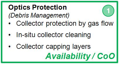
28 Source power and availability drive productivity Technology development work is ongoing to improve all aspects Slide 28 Productivity = Throughput( EUV Power) Availability EUV Power= (CO 2 laser power CE transmission)*(1-dose overhead) Raw EUV power Source power from 10 W to > 250 W Drive laser power from 20 to 40 kw Conversion efficiency (CE) from 1 to 6% Dose margin from 50 to 10% Optical transmission Source availability Automation Collector protection Droplet generator reliability & lifetime Drive laser reliability
29 8kW 10W 45% 12kW 50W 30% 17% 10% 15kW 20kW 100W Laser Power (kw) EUV Power (W) Dose Overhead (%) 210W EUV power scaling through 2016 EUV power ~ CO 2 power * Conversion Efficiency * (1-Dose Overhead) Slide 29 CE=5.5% CE=3.5% CE=2.5% CE=0.8% NOMO and NXE:3100 drive laser MOPA+PP and NXE:3100 drive laser MOPA+PP and NXE:3300B Drive Laser MOPA+PP High Power Amplification Chain


30 Conversion efficiency: Optimizing pre-pulse to create a more efficient Target target expansion fills main pulse beam waist Slide 30 Prepulse (low energy) Mainpulse (high energy) Target shape changes from droplet to disk


31 Conversion efficiency (%) Increased conversion efficiency with Pre-pulse by optimization of target size, shape and density 7 Slide no PP small disk large disk partial-cloud cloud EUV CE ~6% demonstrated on development platforms


32 Plasma scale length (Z) is the key to increase its volume Volume-distributed laser absorption enhances CO 2 laser deposition in plasma Schematic diagram of traditional LPP T e Z absorption ablation n Hydrodynamic simulation of CO 2 Sn LPP T e Z Slide laser n c EUV n e n i Corona Laser Laser, e, ions Energy transport Heat, radiation flow Mass flow SPIE 2016, 97760K-1, Michael Purvis Advances in predictive plasma formation modelling
33 Slide Jan 2016 The Drive Laser, Droplet Generator And collector
 27 30 40 3300 CO 2 drive laser 35000 30000 25000 20000 15000 10000 5000 0 0 50 100 150 200 250 Laser pulse duration")
34 Laser power (W) CO 2 laser power scaling to scale EUV power Efficient CO 2 laser pulse amplification Slide 34 Throughput, WPH EUV power (W) CO 2 lase power (kw) CO 2 drive laser Laser pulse duration (ns)


35 Droplet position, m Droplet Generator, Principle of Operation Tin is loaded in a vessel & heated above melting point Pressure applied by an inert gas Tin flows through a filter prior to the nozzle Tin jet is modulated by mechanical vibrations Slide 35 Sn Gas Filter Modulator Nozzle Pressure: 1005 psi Pressure: Frequency: 30 khz Frequency: 50 khz 140 m 50 m Diameter: 30 m 31 µm Diameter: 37 µm Distance: 1357 µm Velocity: 40.7 m/s 1025 psi Distance: 821 µm Velocity: 41.1 m/s 16 m Pressure: 1025 psi Frequency: 500 khz Diameter: 14 µm Distance: 82 µm Velocity: 40.8 m/s Time, sec Pressure: 1005 psi Frequency: 1706 khz Diameter: 9 µm Distance: 24 µm Velocity: 41.1 m/s Fig. 1. Images of tin droplets obtained with a 5.5 μm nozzle. The images on the left were obtained in frequency modulation regime; the image on the right with a simple sine wave signal. The images were taken at 300 mm distance from the nozzle. Short term droplet position stability σ~1 m


36 Forces on Droplets during EUV Generation Slide 36 High EUV power at high repetition rates drives requirements for higher speed droplets with large space between droplets
 55.2 MPa (121 m/s) 1.5 mm Tin droplets at 80 khz and at different applied pressures.")
37 High Speed Droplet Generation Slide 37 Pressure (Speed) 3.5 MPa (26 m/s) 6.9 MPa (40 m/s) 13.8 MPa (58 m/s) 27.6 MPa (84 m/s) 41.4 MPa (104 m/s) 55.2 MPa (121 m/s) 1.5 mm Tin droplets at 80 khz and at different applied pressures. Images taken at a distance of 200 mm from the nozzle

38 EUV Collector: Normal Incidence Slide 38 Ellipsoidal design Plasma at first focus Power delivered to exposure tool at second focus (intermediate focus) 650 mm diameter Collection solid angle: 5 sterrad Average reflectivity: > 40% Wavelength matching across the entire collection area 5sr Normal Incidence Graded Multilayer Coated Collector
39 Collector Protection EUV collector Temperature controlled DG Hydrogen buffer gas causes deceleration of ions Hydrogen flow away from collector reduces atomic tin deposition rate Slide 39 H 2 flow Laser beam Sn droplet / plasma IF Reaction of H radicals with Sn to form SnH 4, which can be pumped away. Sn (s) + 4H (g) SnH 4 (g) Sn catcher Vessel with vacuum pumping to remove hot gas and tin vapor Internal hardware to collect micro particles
40 Collector Lifetime on NXE Slide %/Gp: observed at a customer About 4 months


41 250W feasibility proven without increase in protective Hydrogen flow No rapid collector contamination, allowing stable droplets and >125 mj/cm² Slide 41 ~200W dose controlled power

42 Summary Significant progress in EUV power scaling, Slide 43 - CE is up to 6 % - Dose-controlled power is up to 210 W CO 2 developments support EUV power scaling, - Clean (spatial and temporal) amplification of short CO 2 laser pulse - High power seed-table enables CO 2 laser power scaling Significant progress made in Source Availability - >80% source availability in the field - >1000 hrs droplet generator runtime - >100 Gp collector lifetime


43 Acknowledgements: Slide 44

44
EUV Source for High Volume Manufacturing: Performance at 250 W and Key Technologies for Power Scaling
 EUV Source for High Volume Manufacturing: Performance at 250 W and Key Technologies for Power Scaling Igor Fomenkov ASML Fellow 2017 Source Workshop, Dublin, Ireland, November 7 th Outline Slide 2 Background
Status and challenges of EUV Lithography
 Status and challenges of EUV Lithography SEMICON Europa Dresden, Germany Jan-Willem van der Horst Product Manager EUV October 10 th, 2013 Slide 2 Contents Introduction NXE:3100 NXE:3300B Summary and acknowledgements
EUV lithography: status, future requirements and challenges
 EUV lithography: status, future requirements and challenges EUVL Dublin Vadim Banine with the help of Rudy Peters, David Brandt, Igor Fomenkov, Maarten van Kampen, Andrei Yakunin, Vladimir Ivanov and many
EUVL Scanners Operational at Chipmakers. Skip Miller Semicon West 2011
 EUVL Scanners Operational at Chipmakers Skip Miller Semicon West 2011 Outline ASML s Lithography roadmap to support Moore s Law Progress on NXE:3100 (0.25NA) EUV systems Progress on NXE:3300 (0.33NA) EUV
EUV lithography: today and tomorrow
 EUV lithography: today and tomorrow Vadim Banine, Stuart Young, Roel Moors Dublin, October 2012 Resolution/half pitch, "Shrink" [nm] EUV DPT ArFi ArF KrF Industry roadmap towards < 10 nm resolution Lithography
EUVL getting ready for volume introduction
 EUVL getting ready for volume introduction SEMICON West 2010 Hans Meiling, July 14, 2010 Slide 1 public Outline ASML s Lithography roadmap to support Moore s Law Progress on 0.25NA EUV systems Progress
LPP EUV Source Development and HVM I Productization
 LPP EUV Source Development and HVM I Productization October 19, 2009 David C. Brandt*, Igor V. Fomenkov, Alex I. Ershov, William N. Partlo, David W. Myers Richard L. Sandstrom, Norbert R. Böwering, Alexander
EUV Light Source The Path to HVM Scalability in Practice
 EUV Light Source The Path to HVM Scalability in Practice Harald Verbraak et al. (all people at XTREME) 2011 International Workshop on EUV and Soft X-ray Sources Nov. 2011 Today s Talk o LDP Technology
EUV Supporting Moore s Law
 EUV Supporting Moore s Law Marcel Kemp Director Investor Relations - Europe DB 2014 TMT Conference London September 4, 2014 Forward looking statements This document contains statements relating to certain
High-NA EUV lithography enabling Moore s law in the next decade
 High-NA EUV lithography enabling Moore s law in the next decade Jan van Schoot, Kars Troost, Alberto Pirati, Rob van Ballegoij, Peter Krabbendam, Judon Stoeldraijer, Erik Loopstra, Jos Benschop, Jo Finders,
TSMC Property. EUV Lithography. The March toward HVM. Anthony Yen. 9 September TSMC, Ltd
 EUV Lithography The March toward HVM Anthony Yen 9 September 2016 1 1 st EUV lithography setup and results, 1986 Si Stencil Mask SR W/C Multilayer Coating Optics λ=11 nm, provided by synchrotron radiation
Discovering Electrical & Computer Engineering. Carmen S. Menoni Professor Week 3 armain.
 Discovering Electrical & Computer Engineering Carmen S. Menoni Professor Week 3 http://www.engr.colostate.edu/ece103/semin armain.html TOP TECH 2012 SPECIAL REPORT IEEE SPECTRUM PAGE 28, JANUARY 2012 P.E.
Bank of America Merrill Lynch Taiwan, Technology and Beyond Conference
 Bank of America Merrill Lynch Taiwan, Technology and Beyond Conference Craig De Young Vice President Investor Relations Taipei, Taiwan March 12, 2013 Forward looking statements Slide 2 Safe Harbor Statement
Holistic View of Lithography for Double Patterning. Skip Miller ASML
 Holistic View of Lithography for Double Patterning Skip Miller ASML Outline Lithography Requirements ASML Holistic Lithography Solutions Conclusions Slide 2 Shrink Continues Lithography keeps adding value
2008 European EUVL. EUV activities the EUVL shop future plans. Rob Hartman
 2008 European EUVL EUV activities the EUVL shop future plans Rob Hartman 2007 international EUVL Symposium 28-31 October 2007 2008 international EUVL Symposium 28 Sapporo, September Japan 1 October 2008
Light Source Technology Advances to Support Process Stability and Performance Predictability for ArF Immersion Double Patterning
 Light Source Technology Advances to Support Process Stability and Performance Predictability for ArF Immersion Double Patterning Ivan Lalovic, Rajasekhar Rao, Slava Rokitski, John Melchior, Rui Jiang,
Laser-Produced Sn-plasma for Highvolume Manufacturing EUV Lithography
 Panel discussion Laser-Produced Sn-plasma for Highvolume Manufacturing EUV Lithography Akira Endo * Extreme Ultraviolet Lithography System Development Association Gigaphoton Inc * 2008 EUVL Workshop 11
Spring of EUVL: SPIE 2012 AL EUVL Conference Review
 Spring of EUVL: SPIE 2012 AL EUVL Conference Review Vivek Bakshi, EUV Litho, Inc., Austin, Texas Monday, February 20, 2012 The SPIE Advanced Lithography EUVL Conference is usually held close to spring,
TWINSCAN XT:1950i Water-based immersion taken to the max Enabling fast, single-exposure lithography at sub 40 nm
 TWINSCAN XT:1950i Water-based immersion taken to the max Enabling fast, single-exposure lithography at sub 40 nm SEMICON West, San Francisco July 14-18, 2008 Slide 1 The immersion pool becomes an ocean
DUV. Matthew McLaren Vice President Program Management, DUV. 24 November 2014
 DUV Matthew McLaren Vice President Program Management, DUV 24 Forward looking statements This document contains statements relating to certain projections and business trends that are forward-looking,
EUV: Status and Challenges Ahead International Workshop on EUVL, Maui 2010
 EUV: Status and Challenges Ahead International Workshop on EUVL, Maui 2010 Jos Benschop Public Agenda Roadmap Status Challenges Summary & conclusion Slide 2 Public Resolution (half pitch) "Shrink" [nm]
Reliable High Power EUV Source Technology for HVM: LPP or DPP? Vivek Bakshi, Ph.D. EUV Litho, Inc.
 Reliable High Power EUV Source Technology for HVM: LPP or DPP? Vivek Bakshi, Ph.D. EUV Litho, Inc. Presentation Outline Source Technology Requirements Source Technology Performance DPP LPP Technology Trend
Nikon EUVL Development Progress Update
 Nikon EUVL Development Progress Update Takaharu Miura EUVL Symposium September 29, 2008 EUVL Symposium 2008 @Lake Tahoe T. Miura September 29, 2008 Slide 1 Presentation Outline 1. Nikon EUV roadmap 2.
Optics for EUV Lithography
 Optics for EUV Lithography Dr. Sascha Migura, Carl Zeiss SMT GmbH, Oberkochen, Germany 2018 EUVL Workshop June 13 th, 2018 Berkeley, CA, USA The resolution of the optical system determines the minimum
Imaging for the next decade
 Imaging for the next decade Martin van den Brink Executive Vice President Products & Technology IMEC Technology Forum 2009 3 June, 2009 Slide 1 Congratulations! ASML and years of making chips better Slide
Metrology in the context of holistic Lithography
 Metrology in the context of holistic Lithography Jeroen Ottens Product System Engineer YieldStar, ASML Lithography is at the heart of chip manufacturing Slide 2 25.April.2017 Repeat 30 to 40 times to build
Lithography Roadmap. without immersion lithography. Node Half pitch. 248nm. 193nm. 157nm EUVL. 3-year cycle: 2-year cycle: imec 2005
 Lithography Roadmap without immersion lithography Node Half pitch 180 nm 130 nm 90 nm 65 nm 45 nm 32 nm 22 nm 250 nm 180 nm 130 nm 90 nm 65 nm 45 nm 32 nm 248nm 193nm 157nm EUVL 3-year cycle: 2-year cycle:
Progress towards Actinic Patterned Mask Inspection. Oleg Khodykin
 Progress towards Actinic Patterned Mask Inspection Oleg Khodykin Outline Status (technical) of EUV Actinic Reticle Inspection program Xe based LPP source as bright and reliable solution Requirements Choice
Laser Produced Plasma Light Source for HVM-EUVL
 Laser Produced Plasma Light Source for HVM-EUVL Akira Endo, Hideo Hoshino, Takashi Suganuma, Krzysztof Nowak, Tatsuya Yanagida, Takayuki Yabu, Takeshi Asayama, Yoshifumi Ueno, Masato Moriya, Masaki Nakano,
EUVL: Challenges to Manufacturing Insertion
 EUVL: Challenges to Manufacturing Insertion Obert R Wood II International Workshop on EUV Lithography CXRO, LBNL, Berkeley, California 14 June 2017 EUV Critical Issues List EUV Critical Issues, as identified
immersion optics Immersion Lithography with ASML HydroLith TWINSCAN System Modifications for Immersion Lithography by Bob Streefkerk
 immersion optics Immersion Lithography with ASML HydroLith by Bob Streefkerk For more than 25 years, many in the semiconductor industry have predicted the end of optical lithography. Recent developments,
Holistic Lithography. Christophe Fouquet. Executive Vice President, Applications. 24 November 2014
 Holistic Lithography Christophe Fouquet Executive Vice President, Applications 24 Holistic Lithography Introduction Customer Problem: Beyond 20nm node scanner and non scanner contributions must be addressed
Update on 193nm immersion exposure tool
 Update on 193nm immersion exposure tool S. Owa, H. Nagasaka, Y. Ishii Nikon Corporation O. Hirakawa and T. Yamamoto Tokyo Electron Kyushu Ltd. January 28, 2004 Litho Forum 1 What is immersion lithography?
Progress in full field EUV lithography program at IMEC
 Progress in full field EUV lithography program at IMEC A.M. Goethals*, G.F. Lorusso*, R. Jonckheere*, B. Baudemprez*, J. Hermans*, F. Iwamoto 1, B.S. Kim 2, I.S. Kim 2, A. Myers 3, A. Niroomand 4, N. Stepanenko
CO 2 / Sn LPP EUV Sources for device development and HVM
 CO 2 / Sn LPP EUV Sources for device development and HVM David C. Brandt, Igor V. Fomenkov, Nigel R. Farrar, Bruno La Fontaine, David W. Myers, Daniel J. Brown, Alex I. Ershov, Richard L. Sandstrom, Georgiy
EUV Lithography Transition from Research to Commercialization
 EUV Lithography Transition from Research to Commercialization Charles W. Gwyn and Peter J. Silverman and Intel Corporation Photomask Japan 2003 Pacifico Yokohama, Kanagawa, Japan Gwyn:PMJ:4/17/03:1 EUV
1 st /2nd generation Laser-Produced Plasma source system for HVM EUV lithography
 1 st /2nd generation Laser-Produced Plasma source system for HVM EUV lithography Hakaru Mizoguchi*1, Tamotsu Abe, Yukio Watanabe, Takanobu Ishihara, Takeshi Ohta,Tsukasa Hori, Tatsuya Yanagida, Hitoshi
UV Nanoimprint Stepper Technology: Status and Roadmap. S.V. Sreenivasan Sematech Litho Forum May 14 th, 2008
 UV Nanoimprint Stepper Technology: Status and Roadmap S.V. Sreenivasan Sematech Litho Forum May 14 th, 2008 Overview Introduction Stepper technology status: Patterning and CD Control Through Etch Alignment
22nm node imaging and beyond: a comparison of EUV and ArFi double patterning
 22nm node imaging and beyond: a comparison of EUV and ArFi double patterning ASML: Eelco van Setten, Orion Mouraille, Friso Wittebrood, Mircea Dusa, Koen van Ingen-Schenau, Jo Finders, Kees Feenstra IMEC:
Light Sources for High Volume Metrology and Inspection Applications
 Light Sources for High Volume Metrology and Inspection Applications Reza Abhari International Workshop on EUV and Soft X- Ray Sources November 9-11, 2015, Dublin, Ireland Reza S. Abhari 11/10/15 1 Inspection
Japan Update. EUVA (Extreme Ultraviolet Lithography System Development Association) Koichi Toyoda. SOURCE TWG 2 March, 2005 San Jose
 Koichi Toyoda. SOURCE TWG 2 March, 2005 San Jose") 1 Japan Update EUVA (Extreme Ultraviolet Lithography System Development Association) Koichi Toyoda SOURCE TWG 2 March, 2005 San Jose Outline 2 EUVA LPP at Hiratsuka R&D Center GDPP at Gotenba Branch Lab.
1 Japan Update EUVA (Extreme Ultraviolet Lithography System Development Association) Koichi Toyoda SOURCE TWG 2 March, 2005 San Jose Outline 2 EUVA LPP at Hiratsuka R&D Center GDPP at Gotenba Branch Lab.
IMEC update. A.M. Goethals. IMEC, Leuven, Belgium
 IMEC update A.M. Goethals IMEC, Leuven, Belgium Outline IMEC litho program overview ASML ADT status 1 st imaging Tool description Resist projects Screening using interference litho K LUP / Novel resist
Mask Technology Development in Extreme-Ultraviolet Lithography
 Mask Technology Development in Extreme-Ultraviolet Lithography Anthony Yen September 6, 2013 Projected End of Optical Lithography 2013 TSMC, Ltd 1976 1979 1982 1985 1988 1991 1994 1997 2000 2003 2007 2012
From ArF Immersion to EUV Lithography
 From ArF Immersion to EUV Lithography Luc Van den hove Vice President IMEC Outline Introduction 193nm immersion lithography EUV lithography Global collaboration Conclusions Lithography is enabling 1000
Newer process technology (since 1999) includes :
 includes :") Newer process technology (since 1999) includes : copper metalization hi-k dielectrics for gate insulators si on insulator strained silicon lo-k dielectrics for interconnects Immersion lithography for masks
Newer process technology (since 1999) includes : copper metalization hi-k dielectrics for gate insulators si on insulator strained silicon lo-k dielectrics for interconnects Immersion lithography for masks
S26 Basic research on 6.x nm EUV generation by laser produced plasma
 S26 Basic research on 6.x nm EUV generation by laser produced plasma Tsukasa Hori, Tatsuya Yanagida, Hitoshi Nagano, Yasunori Wada, Soumagne Georg, Junichi Fujimoto*, Hakaru Mizoguchi* e-mail : tsukasa_hori@komatsu.co.jp
MAPPER: High throughput Maskless Lithography
 MAPPER: High throughput Maskless Lithography Marco Wieland CEA- Leti Alterative Lithography workshop 1 Today s agenda Introduction Applications Qualification of on-tool metrology by in-resist metrology
Development Status of EUV Sources for Use in Alpha-, Beta- and High Volume Chip Manufacturing Tools
 Development Status of EUV Sources for Use in Alpha-, Beta- and High Volume Chip Manufacturing Tools Uwe Stamm, Jürgen Kleinschmidt, Bernd Nikolaus, Guido Schriever, Max Christian Schürmann, Christian Ziener
Scope and Limit of Lithography to the End of Moore s Law
 Scope and Limit of Lithography to the End of Moore s Law Burn J. Lin tsmc, Inc. 1 What dictate the end of Moore s Law Economy Device limits Lithography limits 2 Litho Requirement of Critical Layers Logic
R&D Status and Key Technical and Implementation Challenges for EUV HVM
 R&D Status and Key Technical and Implementation Challenges for EUV HVM Sam Intel Corporation Agenda Requirements by Process Node EUV Technology Status and Gaps Photoresists Tools Reticles Summary 2 Moore
NXE: 3300B qualified to support customer product development
 ASML s customer magazine 2013 Issue 2 Extending the TWINSCAN NXT platform Computational lithography enables device scaling NXE: 3300B qualified to support customer product development 4 8 10 4 NXE:3300B
Competitive in Mainstream Products
 Competitive in Mainstream Products Bert Koek VP, Business Unit manager 300mm Fabs Analyst Day 20 September 2005 ASML Competitive in mainstream products Introduction Market share Device layers critical
1 st generation Laser-Produced Plasma source system for HVM EUV lithography
 1 st generation Laser-Produced Plasma source system for HVM EUV lithography Hakaru Mizoguchi *1, Tamotsu Abe, Yukio Watanabe, Takanobu Ishihara, Takeshi Ohta, Tsukasa Hori, Akihiko Kurosu, Hiroshi Komori,
Imec pushes the limits of EUV lithography single exposure for future logic and memory
 Edition March 2018 Semiconductor technology & processing Imec pushes the limits of EUV lithography single exposure for future logic and memory Imec has made considerable progress towards enabling extreme
Optical Microlithography XXVIII
 PROCEEDINGS OF SPIE Optical Microlithography XXVIII Kafai Lai Andreas Erdmann Editors 24-26 February 2015 San Jose, California, United States Sponsored by SPIE Cosponsored by Cymer, an ASML company (United
Power scaling of picosecond thin disc laser for LPP and FEL EUV sources
 Power scaling of picosecond thin disc laser for LPP and FEL EUV sources A. Endo 1,2, M. Smrz 1, O. Novak 1, T. Mocek 1, K.Sakaue 2 and M.Washio 2 1) HiLASE Centre, Institute of Physics AS CR, Dolní Břežany,
Fiber Lasers for EUV Lithography
 Fiber Lasers for EUV Lithography A. Galvanauskas, Kai Chung Hou*, Cheng Zhu CUOS, EECS Department, University of Michigan P. Amaya Arbor Photonics, Inc. * Currently with Cymer, Inc 2009 International Workshop
Process Optimization
 Process Optimization Process Flow for non-critical layer optimization START Find the swing curve for the desired resist thickness. Determine the resist thickness (spin speed) from the swing curve and find
Multiple Patterning for Immersion Extension and EUV Insertion. Chris Bencher Distinguished Member of Technical Staff Applied Materials CTO group
 Multiple Patterning for Immersion Extension and EUV Insertion Chris Bencher Distinguished Member of Technical Staff Applied Materials CTO group Abstract Multiple Patterning for Immersion Extension and
Light Sources for EUV Mask Metrology. Heiko Feldmann, Ulrich Müller
 Light Sources for EUV Mask Metrology Heiko Feldmann, Ulrich Müller Dublin, October 9, 2012 Agenda 1 2 3 4 Actinic Metrology in Mask Making The AIMS EUV Concept Metrology Performance Drivers and their Relation
Enabling Semiconductor Innovation and Growth
 Enabling Semiconductor Innovation and Growth EUV lithography drives Moore s law well into the next decade BAML 2018 APAC TMT Conference Taipei, Taiwan Craig De Young Vice President IR - Asia IR March 14,
Section 2: Lithography. Jaeger Chapter 2. EE143 Ali Javey Slide 5-1
 Section 2: Lithography Jaeger Chapter 2 EE143 Ali Javey Slide 5-1 The lithographic process EE143 Ali Javey Slide 5-2 Photolithographic Process (a) (b) (c) (d) (e) (f) (g) Substrate covered with silicon
The future of EUVL. Outline. by Winfried Kaiser, Udo Dinger, Peter Kuerz, Martin Lowisch, Hans-Juergen Mann, Stefan Muellender,
 The future of EUVL by Winfried Kaiser, Udo Dinger, Peter Kuerz, Martin Lowisch, Hans-Juergen Mann, Stefan Muellender, William H. Arnold, Jos Benshop, Steven G. Hansen, Koen van Ingen-Schenau Outline Introduction
EUVL Activities in China
 2014 EUVL Workshop EUVL Activities in China Yanqiu Li, Zhen Cao Beijing Institute of Technology (BIT) Email: liyanqiu@bit.edu.cn Activities only refer to published papers June 25, 2014 OUTLINE Overview
Novel EUV Resist Development for Sub-14nm Half Pitch
 EUV Workshop 2015 Maui, HI P64 Novel EUV Resist Development for Sub-14nm Half Pitch Yoshi Hishiro JSR Micro Inc. EUV Workshop, June 17, 2015 1 Contents Requirement for sub-14nm HP EUV resist JSR strategy
Present Status and Future Prospects of EUV Lithography
 3rd EUV-FEL Workshop Present Status and Future Prospects of EUV Lithography (EUV リソグラフィーの現状と将来展望 ) December 11, 2011 Evolving nano process Infrastructure Development Center, Inc. (EIDEC) Hidemi Ishiuchi
Closed Loop Registration Control (RegC ) Using PROVE as the Data Source for the RegC Process
 Using PROVE as the Data Source for the RegC Process") Invited Paper Closed Loop Registration Control (RegC ) Using PROVE as the Data Source for the RegC Process Erez Graitzer 1 ; Avi Cohen 1 ; Vladimir Dmitriev 1 ; Itamar Balla 1 ; Dan Avizemer 1 Dirk Beyer
Invited Paper Closed Loop Registration Control (RegC ) Using PROVE as the Data Source for the RegC Process Erez Graitzer 1 ; Avi Cohen 1 ; Vladimir Dmitriev 1 ; Itamar Balla 1 ; Dan Avizemer 1 Dirk Beyer
A Comparison of ArF and KrF Laser Performance At 2kHz For Microlithography
 A Comparison of ArF and KrF Laser Performance At 2kHz For Microlithography Herve Besaucele, Palash Das, Thomas Duffey, Todd Embree, Alex Ershov, Vladimir Fleurov, Steve Grove, Paul Meleher, Richard Ness,
Actinic Review of EUV Masks: Performance Data and Status of the AIMS TM EUV System
 Actinic Review of EUV Masks: Performance Data and Status of the AIMS TM EUV System Dirk Hellweg*, Markus Koch, Sascha Perlitz, Martin Dietzel, Renzo Capelli Carl Zeiss SMT GmbH, Rudolf-Eber-Str. 2, 73447
Electron Multi-Beam Technology for Mask and Wafer Direct Write. Elmar Platzgummer IMS Nanofabrication AG
 Electron Multi-Beam Technology for Mask and Wafer Direct Write Elmar Platzgummer IMS Nanofabrication AG Contents 2 Motivation for Multi-Beam Mask Writer (MBMW) MBMW Tool Principles and Architecture MBMW
EUVL Activities in China. Xiangzhao Wang Shanghai Inst. Of Opt. and Fine Mech. Of CAS. (SIOM) Shanghai, China.
 Shanghai, China.") EUVL Activities in China Xiangzhao Wang Shanghai Inst. Of Opt. and Fine Mech. Of CAS. (SIOM) Shanghai, China. wxz26267@siom.ac.cn Projection Optics Imaging System Surface Testing Optical Machining ML Coating
EUVL Activities in China Xiangzhao Wang Shanghai Inst. Of Opt. and Fine Mech. Of CAS. (SIOM) Shanghai, China. wxz26267@siom.ac.cn Projection Optics Imaging System Surface Testing Optical Machining ML Coating
PROCEEDINGS OF SPIE. LPP-EUV light source for HVM lithography. T. Saito, Y. Ueno, T. Yabu, A. Kurosawa, S. Nagai, et al.
 PROCEEDINGS OF SPIE SPIEDigitalLibrary.org/conference-proceedings-of-spie LPP-EUV light source for HVM lithography T. Saito, Y. Ueno, T. Yabu, A. Kurosawa, S. Nagai, et al. Invited Paper LPP-EUV light
Immersion Lithography: New Opportunities for Semiconductor Manufacturing
 Immersion Lithography: New Opportunities for Semiconductor Manufacturing Tim Brunner, Dario Gil, Carlos Fonseca and Nakgeuon Seong IBM - SRDC Bob Streefkerk, Christian Wagner and Marco Stavenga ASML Outline
Section 2: Lithography. Jaeger Chapter 2 Litho Reader. EE143 Ali Javey Slide 5-1
 Section 2: Lithography Jaeger Chapter 2 Litho Reader EE143 Ali Javey Slide 5-1 The lithographic process EE143 Ali Javey Slide 5-2 Photolithographic Process (a) (b) (c) (d) (e) (f) (g) Substrate covered
Benefit of ArF immersion lithography in 55 nm logic device manufacturing
 Benefit of ArF immersion lithography in 55 nm logic device manufacturing Takayuki Uchiyama* a, Takao Tamura a, Kazuyuki Yoshimochi a, Paul Graupner b, Hans Bakker c, Eelco van Setten c, Kenji Morisaki
Towards an affordable Cost of Ownership for EUVL. Melissa Shell Principal Engineer & Program Manager, EUVL Research Components Research October 2006
 Towards an affordable Cost of Ownership for EUVL Melissa Shell Principal Engineer & Program Manager, EUVL Research Components Research October 2006 1 Robert Bristol Heidi Cao Manish Chandhok Michael Leeson
2009 International Workshop on EUV Lithography
 Contents Introduction Absorber Stack Optimization Non-flatness Correction Blank Defect and Its Mitigation Wafer Printing Inspection Actinic Metrology Cleaning and Repair Status Remaining Issues in EUV
Improving efficiency of CO 2
 Improving efficiency of CO 2 Laser System for LPP Sn EUV Source K.Nowak*, T.Suganuma*, T.Yokotsuka*, K.Fujitaka*, M.Moriya*, T.Ohta*, A.Kurosu*, A.Sumitani** and J.Fujimoto*** * KOMATSU ** KOMATSU/EUVA
450mm and Moore s Law Advanced Packaging Challenges and the Impact of 3D
 450mm and Moore s Law Advanced Packaging Challenges and the Impact of 3D Doug Anberg VP, Technical Marketing Ultratech SOKUDO Lithography Breakfast Forum July 10, 2013 Agenda Next Generation Technology
Section 2: Lithography. Jaeger Chapter 2 Litho Reader. The lithographic process
 Section 2: Lithography Jaeger Chapter 2 Litho Reader The lithographic process Photolithographic Process (a) (b) (c) (d) (e) (f) (g) Substrate covered with silicon dioxide barrier layer Positive photoresist
GIGAPHOTON INTRODUCTION
 GIGAPHOTON INTRODUCTION 15 th September 2017 Tatsuo Enami Director and Senior Executive Officer GIGAPHOTON Copyright Gigaphoton Inc. Outline of Gigaphoton Business Light source business
Major Fabrication Steps in MOS Process Flow
 Major Fabrication Steps in MOS Process Flow UV light Mask oxygen Silicon dioxide photoresist exposed photoresist oxide Silicon substrate Oxidation (Field oxide) Photoresist Coating Mask-Wafer Alignment
Lithography. 3 rd. lecture: introduction. Prof. Yosi Shacham-Diamand. Fall 2004
 Lithography 3 rd lecture: introduction Prof. Yosi Shacham-Diamand Fall 2004 1 List of content Fundamental principles Characteristics parameters Exposure systems 2 Fundamental principles Aerial Image Exposure
Shooting for the 22nm Lithography Goal with the. Coat/Develop Track. SOKUDO Lithography Breakfast Forum 2010 July 14 (L1)
") Shooting for the 22nm Lithography Goal with the Coat/Develop Track SOKUDO Lithography Breakfast Forum 2010 July 14 (L1) Three (3) different exposure options for 22nm: Public External (L1) MAPPER Lithography
Shooting for the 22nm Lithography Goal with the Coat/Develop Track SOKUDO Lithography Breakfast Forum 2010 July 14 (L1) Three (3) different exposure options for 22nm: Public External (L1) MAPPER Lithography
Lecture 7. Lithography and Pattern Transfer. Reading: Chapter 7
 Lecture 7 Lithography and Pattern Transfer Reading: Chapter 7 Used for Pattern transfer into oxides, metals, semiconductors. 3 types of Photoresists (PR): Lithography and Photoresists 1.) Positive: PR
EUV Substrate and Blank Inspection
 EUV Substrate and Blank Inspection SEMATECH EUV Workshop 10/11/99 Steve Biellak KLA-Tencor RAPID Division *This work is partially funded by NIST-ATP project 98-06, Project Manager Purabi Mazumdar 1 EUV
Optical Lithography. Here Is Why. Burn J. Lin SPIE PRESS. Bellingham, Washington USA
 Optical Lithography Here Is Why Burn J. Lin SPIE PRESS Bellingham, Washington USA Contents Preface xiii Chapter 1 Introducing Optical Lithography /1 1.1 The Role of Lithography in Integrated Circuit Fabrication
Institute of Solid State Physics. Technische Universität Graz. Lithography. Peter Hadley
 Technische Universität Graz Institute of Solid State Physics Lithography Peter Hadley http://www.cleanroom.byu.edu/virtual_cleanroom.parts/lithography.html http://www.cleanroom.byu.edu/su8.phtml Spin coater
Multi-pass Slab CO 2 Amplifiers for Application in EUV Lithography
 Multi-pass Slab CO 2 Amplifiers for Application in EUV Lithography V. Sherstobitov*, A. Rodionov**, D. Goryachkin*, N. Romanov*, L. Kovalchuk*, A. Endo***, K. Nowak*** *JSC Laser Physics, St. Petersburg,
EUV Resist Materials and Process for 16 nm Half Pitch and Beyond
 EUV Workshop 2013 June 13, 2013 EUV Resist Materials and Process for 16 nm Half Pitch and Beyond Yoshi Hishiro JSR Micro Inc. No13-2400-056 Challenge for EUV Resist & JSR approaches EUV Resist Resolution,
450mm patterning out of darkness Backend Process Exposure Tool SOKUDO Lithography Breakfast Forum July 10, 2013 Doug Shelton Canon USA Inc.
 450mm patterning out of darkness Backend Process Exposure Tool SOKUDO Lithography Breakfast Forum 2013 July 10, 2013 Doug Shelton Canon USA Inc. Introduction Half Pitch [nm] 2013 2014 2015 2016 2017 2018
Leadership Through Innovation Litho for the future
 Leadership Through Innovation Litho for the future Deutsche Bank Access Asia Conference 2010 Singapore Craig De Young VP Investor Relations and Corporate Communications May 12, 2010 Public Safe Harbor
TECHNOLOGY ROADMAP 2006 UPDATE LITHOGRAPHY FOR
 INTERNATIONAL TECHNOLOGY ROADMAP FOR SEMICONDUCTORS 2006 UPDATE LITHOGRAPHY THE ITRS IS DEVISED AND INTENDED FOR TECHNOLOGY ASSESSMENT ONLY AND IS WITHOUT REGARD TO ANY COMMERCIAL CONSIDERATIONS PERTAINING
EE143 Fall 2016 Microfabrication Technologies. Lecture 3: Lithography Reading: Jaeger, Chap. 2
 EE143 Fall 2016 Microfabrication Technologies Lecture 3: Lithography Reading: Jaeger, Chap. 2 Prof. Ming C. Wu wu@eecs.berkeley.edu 511 Sutardja Dai Hall (SDH) 1-1 The lithographic process 1-2 1 Photolithographic
ECSE 6300 IC Fabrication Laboratory Lecture 3 Photolithography. Lecture Outline
 ECSE 6300 IC Fabrication Laboratory Lecture 3 Photolithography Prof. James J. Q. Lu Bldg. CII, Rooms 6229 Rensselaer Polytechnic Institute Troy, NY 12180 Tel. (518)276 2909 e mails: luj@rpi.edu http://www.ecse.rpi.edu/courses/s18/ecse
LPP collector mirrors coating, metrology and refurbishment
 LPP collector mirrors coating, metrology and refurbishment 2013 International Workshop on EUV and soft X-Ray Sources Torsten Feigl, Marco Perske, Hagen Pauer, Tobias Fiedler optix fab GmbH Christian Laubis,
EUVL: Challenges to Manufacturing Insertion
 Journal of Photopolymer Science and Technology Volume 30, Number 5 (2017) 599-604 C 2017SPST Technical Paper EUVL: Challenges to Manufacturing Insertion Obert R. Wood II * Strategic Lithography Technology,
Part 5-1: Lithography
 Part 5-1: Lithography Yao-Joe Yang 1 Pattern Transfer (Patterning) Types of lithography systems: Optical X-ray electron beam writer (non-traditional, no masks) Two-dimensional pattern transfer: limited
Akira Miyake, Chidane Ouchi, International EUVL Symposium, October , Kobe Slide 1
 Development Status of Canon s EUVL Exposure Tool Akira Miyake, Chidane Ouchi, Hideki Morishima, and Hiroyoshi Kubo Canon Inc. International EUVL Symposium, October 18 2010, Kobe Slide 1 Outline EUVL Exposure
A Reliable Higher Power ArF Laser with Advanced Functionality for Immersion Lithography
 A Reliable Higher Power ArF Laser with Advanced Functionality for Immersion Lithography Akihiko Kurosu, Masaki Nakano, Masanori Yashiro, Masaya Yoshino, Hiroaki Tsushima, Hiroyuki Masuda, Takahito Kumazaki,