Present Status and Future Prospects of EUV Lithography
|
|
|
- William Clark
- 5 years ago
- Views:
Transcription
1 3rd EUV-FEL Workshop Present Status and Future Prospects of EUV Lithography (EUV リソグラフィーの現状と将来展望 ) December 11, 2011 Evolving nano process Infrastructure Development Center, Inc. (EIDEC) Hidemi Ishiuchi 1
2 Outline Scaling Trend: End of Moore s Law? Present Status of EUV Lithography Challenges in EUV Lithography Mass Production with EUV Lithography Summary 2
3 IRDS Lithography Roadmap YEAR OF PRODUCTION DRAM DRAM minimum ½ pitch (nm) Flash 2D Flash ½ pitch (nm) (un-contacted poly) D NAND minimum array 1/2 pitch (nm) <80 <80 <80 <80 MPU / Logic Logic industry "Node Range" Labeling (nm) "10" "7" "5" "3" "2.1" "1.5" "1.0" MPU/ASIC Minimum Metal ½ pitch (nm) Physical Gate Length for HP Logic (nm) No scaling needed after2027 or 2030? DRAM still shrinking Flash is no longer a driver for high resolution patterning Logic is driving patterning Lateral Gate All Around (LGAA) 1/2 pitch Vertical Gate All Around (VGAA) half pitch (nm) Vertical GAA Diameter (nm) Chip size (mm 2 ) Maximum exposure field height (mm) Maximum exposure field length, i.e. scanning direction (mm) Maximum field area printed by exposure tool (mm 2 ) Small holes for VGAA High-NA(0.55) EUV exposure tool with a reduced field size: 858 mm 2 429mm 2 Source: IRDS 2017 Edition, Lithography, Table LITH-1 (2018) Manufacturable solutions exist, and are being optimized Manufacturable solutions are known Interim solutions are known Manufacturable solutions are NOT known 3
 Floating Gate Cell (intel / Micron)")
4 3D Cell Arrays of NAND Flash Memories Charge Trap Cell (Samsung) Floating Gate Cell (intel / Micron) 4

5 Contact hole pattern in DRAM EUV single exposure process can be applied below D1z node or beyond. Source: Mijuing Lim et al., EUV contact-hole local CD uniformity optimization for DRAM storage node application, SPIE Advanced Lithography, 2018; Proc. SPIE 10583, Extreme Ultraviolet (EUV) Lithography IX, X (1 May 2018); doi: /
")
6 More Complex MOSFET Structure (ITRS 2015) 6

7 Multiple Patterning with ArF immersion tools Source: ITRS 2013 Edition, Lithography, Figure LITH2 7

8 EUV vs ArF immersion: process complexity Source: nvestor_day_2016_euv_and_its_business_opportunity_hmeiling.pdf 8

9 ASML NXE:3400 System Source: ASML Homepage, Image Library, 9
10 EUV Source Power Source: Roderik van Es et al., EUV for HVM: towards and industrialized scanner for HVM NXE3400B performance update, SPIE Advanced Lithography,

11 High-NA projection optics Source: J. van School et al., High-NA EUV Lithography enabling Moore s law in the next decade, SPIE Photomask Technology + EUV Lithography,

12 High-NA Surface Metrology Source: J. van School et al., High-NA EUV Lithography enabling Moore s law in the next decade, SPIE Photomask Technology + EUV Lithography,
13 7 nm Technologies in IEDM 2016 IBM, GLOBALFOUNDRIES, and Samsung: Poly Si (contacted): 44nm / 48 nm pitch (ArF-i) Metal interconnect: 36nm pitch (EUV) EUV lithography for Metal Interconnect TSMC: SRAM cell size: um 2 Poly Si (contacted):?? nm pitch Metal interconnect:?? nm pitch ArF immersion (ArF-i) lithography (R&D with EUV Lithography, too) Ref: IEDM Technical Digest, 2016, Dec.,

14 IEDM 2016, #2.7 IBM/GF/Samsung Source: R. Xie, et al, A 7nm FinFET Technology Featuring EUV Patterning and Dual Strained High Mobility Channels, IEDM Technical Digest, pp.47-50, pp,


15 IEDM 2016, #2.7 IBM/GF/Samsung Source: R. Xie, et al, A 7nm FinFET Technology Featuring EUV Patterning and Dual Strained High Mobility Channels, IEDM Technical Digest, pp.47-50, pp,
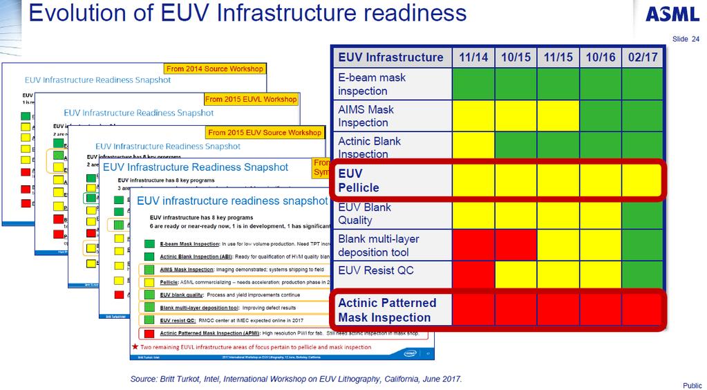
16 EUV Infrastructure Readiness Source: 16

17 Reticle Front-Side Defects Source: A. Yen, Continued Scaling in Semiconductor Manufacturing with EUV Lithography, 2018 EUVL Workshop,

18 Defect Performance on EUV Scanners Source: Roderik van Es et al., EUV for HVM: towards and industrialized scanner for HVM NXE3400B performance update, SPIE Advanced Lithography,

19 Pellicle for EUV Mask Source: Roderik van Es et al., EUV for HVM: towards and industrialized scanner for HVM NXE3400B performance update, SPIE Advanced Lithography,

20 Lasertec s Mask Inspection Tools Source: Lasertec Corporation, First Half of Fiscal Year ending June 2018 Financial Results, Feb. 7,

21 Stochastic Effects in EUV Lithography Source: P. De Bisshop and E. Hendrickx, Stochastic effects in EUV lithography, SPIE Advanced Lithography, Proc. SPIE 10583, Extreme Ultraviolet (EUV) Lithography IX, K, doi: /
22 Stochastic Effects in EUV Lithography Source: P. De Bisshop and E. Hendrickx, Stochastic effects in EUV lithography, SPIE Advanced Lithography, Proc. SPIE 10583, Extreme Ultraviolet (EUV) Lithography IX, K, doi: /

23 EUV-FEL (Free Electron Laser) Source: H. Kawata, Strategy to realize the EUV-FEL high power light source, 2016 International Symposium on Extreme Ultraviolet Lithography, Hiroshima, Japan, Oct. 24,
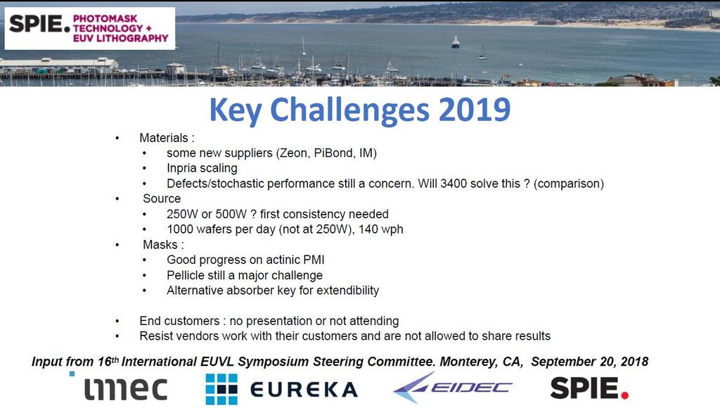
24 Key Challenges 24

25 EUV Focus Areas Source: Closing Address, SPIE Photomask Technology + EUV Lithography 2018, Monterey, U.S.A., Sept. 20,

26 EUV Focus Areas Source: Closing Address, SPIE Photomask Technology + EUV Lithography 2018, Monterey, U.S.A., Sept. 20,

27 EUV Focus Areas Source: Closing Address, SPIE Photomask Technology + EUV Lithography 2018, Monterey, U.S.A., Sept. 20,
28 EUV Focus Areas Source: Closing Address, SPIE Photomask Technology + EUV Lithography 2018, Monterey, U.S.A., Sept. 20,

29 Mass production with EUV Source: _Investor_Day_2016_EUV_and_its_Business_Opportunity_HMeiling.pdf 29
30 Mass Production with EUV: TSMC TSMC to Start 5nm Production in April 5 October 2018 SAN JOSE, Calif. TSMC taped out its first chip in a process making limited use of extreme ultraviolet lithography and will start risk production in April on a 5- nm node with full EUV. In process technology, TSMC announced that it taped out a customer chip in an N7+ node that can use EUV on up to four layers. Its N5 that will use EUV on up to 14 layers will be ready for risk production in April. EUV aims to lower costs by reducing the number of masks required for leading-edge designs 年 4 月に EUV による 5nm 世代のリスク生産を開始 N7+ 世代では EUV を 4 層まで利用可 N5 世代では EUV を 14 層まで利用可 Source: EE Times Asia tsmc-to-start-5nm-production-in-april 30
31 Mass Production with EUV: Samsung Samsung Ramps 7nm EUV Chips 17 October 2018 SAN JOSE, Calif. The race is on to get the first chip made with extreme ultraviolet lithography out the foundry door. Samsung said it has taped out and is ramping multiple 7nm chips using EUV following a similar announcement earlier this month from its larger foundry rival TSMC. In its core memory business, Samsung said that it is sampling 256-GByte RDIMMs made with its 16-Gbit chips. The chips are made in a 1y-nm process first described a year ago. It was not clear whether EUV is being applied to the 1y process. However, follow-on 1z and 1a nodes will increasingly use EUV, suggested Samsung s head of DRAM development, Seong Jin Jang, in a talk here. Source: EE Times EUV を使って複数の 7nm( ロジック ) チップの量産開始 1y 世代の 16Gbit DRAM チップによる 256GByte RDIMM* をサンプリング中 この世代で EUV が使われているかどうかはわからない 1z と 1a 世代の DRAM では EUV の利用が増えると発言 * RDIMM: registered dual in-line memory module の略 Registered Buffer を内臓したメモリモジュール サーバなどで使われる 31
32 Summary EUV source power of 250W has been achieved. Key challenges in EUV Lithography are pellicle, actinic pattern inspection, stochastics, etc. EUV lithography will be used in mass production tool for 7nm or 5nm logic products and beyond. EUV-FEL is a possible solution as an EUV source with higher average power than 1 kw. Its cost of ownership, peak power, coherence of the EUV-FEL source might be the potential problems to be solved 32
33 Glossary CD: DP: DSA: EUVL: LER: LWR: ML: NA: IRDS: ITRS: SADP: SAQP: QP: SP: Critical Dimension Double Patterning Directed Self Assembly Extreme Ultraviolet Lithography Line Edge Roughness Line Width Roughness Maskless Lithography Numerical Aperture International Roadmap for Devices and Systems International Technology Roadmap for Semiconductors Self Aligned Double Patterning Self Aligned Quadruple Patterning Quadruple Patterning Quadruple Patterning 33
Scaling of Semiconductor Integrated Circuits and EUV Lithography
 Scaling of Semiconductor Integrated Circuits and EUV Lithography ( 半導体集積回路の微細化と EUV リソグラフィー ) December 13, 2016 EIDEC (Emerging nano process Infrastructure Development Center, Inc.) Hidemi Ishiuchi 1 OUTLINE
Multiple Patterning for Immersion Extension and EUV Insertion. Chris Bencher Distinguished Member of Technical Staff Applied Materials CTO group
 Multiple Patterning for Immersion Extension and EUV Insertion Chris Bencher Distinguished Member of Technical Staff Applied Materials CTO group Abstract Multiple Patterning for Immersion Extension and
(Complementary E-Beam Lithography)
") Extending Optical Lithography with C E B L (Complementary E-Beam Lithography) July 13, 2011 4008 Burton Drive, Santa Clara, CA 95054 Outline Complementary Lithography E-Beam Complements Optical Multibeam
Extending Optical Lithography with C E B L (Complementary E-Beam Lithography) July 13, 2011 4008 Burton Drive, Santa Clara, CA 95054 Outline Complementary Lithography E-Beam Complements Optical Multibeam
EUVL getting ready for volume introduction
 EUVL getting ready for volume introduction SEMICON West 2010 Hans Meiling, July 14, 2010 Slide 1 public Outline ASML s Lithography roadmap to support Moore s Law Progress on 0.25NA EUV systems Progress
アルゴリズムの設計と解析. 教授 : 黄潤和 (W4022) SA: 広野史明 (A4/A8)
 SA: 広野史明 (A4/A8)") アルゴリズムの設計と解析 教授 : 黄潤和 (W4022) rhuang@hosei.ac.jp SA: 広野史明 (A4/A8) fumiaki.hirono.5k@stu.hosei.ac.jp Divide and Conquer Dynamic Programming L3. 動的計画法 Dynamic Programming What is dynamic programming? Dynamic
アルゴリズムの設計と解析 教授 : 黄潤和 (W4022) rhuang@hosei.ac.jp SA: 広野史明 (A4/A8) fumiaki.hirono.5k@stu.hosei.ac.jp Divide and Conquer Dynamic Programming L3. 動的計画法 Dynamic Programming What is dynamic programming? Dynamic
TSMC Property. EUV Lithography. The March toward HVM. Anthony Yen. 9 September TSMC, Ltd
 EUV Lithography The March toward HVM Anthony Yen 9 September 2016 1 1 st EUV lithography setup and results, 1986 Si Stencil Mask SR W/C Multilayer Coating Optics λ=11 nm, provided by synchrotron radiation
The future of lithography and its impact on design
 The future of lithography and its impact on design Chris Mack www.lithoguru.com 1 Outline History Lessons Moore s Law Dennard Scaling Cost Trends Is Moore s Law Over? Litho scaling? The Design Gap The
Intermediate Conversation Material #10
 Intermediate Conversation Material #10 OUR AGENDA FOR TODAY At work Exercise 1: Picture Conversation A. Read the dialogue below. 次の会話を読んでみましょう Ms. Jefferson, what s our agenda for today s meeting? Our
Mask Technology Development in Extreme-Ultraviolet Lithography
 Mask Technology Development in Extreme-Ultraviolet Lithography Anthony Yen September 6, 2013 Projected End of Optical Lithography 2013 TSMC, Ltd 1976 1979 1982 1985 1988 1991 1994 1997 2000 2003 2007 2012
EUV lithography: today and tomorrow
 EUV lithography: today and tomorrow Vadim Banine, Stuart Young, Roel Moors Dublin, October 2012 Resolution/half pitch, "Shrink" [nm] EUV DPT ArFi ArF KrF Industry roadmap towards < 10 nm resolution Lithography
EUVL: Challenges to Manufacturing Insertion
 EUVL: Challenges to Manufacturing Insertion Obert R Wood II International Workshop on EUV Lithography CXRO, LBNL, Berkeley, California 14 June 2017 EUV Critical Issues List EUV Critical Issues, as identified
Lesson 5 What The Last Supper Tells Us
 Lesson 5 What The Last Supper Tells Us Part 1 What is Leonardo Da Vinci s The Last Supper Known as? レオナルド ダ ヴィンチの 最後の晩餐 はどんなものとして知られているのか? The Last Supper is one of/ the most famous religious subjects.//
450mm and Moore s Law Advanced Packaging Challenges and the Impact of 3D
 450mm and Moore s Law Advanced Packaging Challenges and the Impact of 3D Doug Anberg VP, Technical Marketing Ultratech SOKUDO Lithography Breakfast Forum July 10, 2013 Agenda Next Generation Technology
Limitations and Challenges to Meet Moore's Law
 Limitations and Challenges to Meet Moore's Law Sept 10, 2015 Sung Kim sung_kim@amat.com State of the art: cleanroom toolsets metrology analysis module development test & reliability Introduction Why do
Omochi rabbit amigurumi pattern
 Omochi rabbit amigurumi pattern うさぎのあみぐるみ Materials Yarn: 1 main color (MC) and 1 contrasting color (CC), as needed. You can make this rabbit toy with any yarn weight, but the yarn colors used per one
EUVL Scanners Operational at Chipmakers. Skip Miller Semicon West 2011
 EUVL Scanners Operational at Chipmakers Skip Miller Semicon West 2011 Outline ASML s Lithography roadmap to support Moore s Law Progress on NXE:3100 (0.25NA) EUV systems Progress on NXE:3300 (0.33NA) EUV
PUSHING LITHOGRAPHY TO ENABLE ULTIMATE NANO-ELECTRONICS. LUC VAN DEN HOVE President & CEO imec
 PUSHING LITHOGRAPHY TO ENABLE ULTIMATE NANO-ELECTRONICS LUC VAN DEN HOVE President & CEO imec OUTLINE! Industry drivers! Roadmap extension! Lithography options! Innovation through global collaboration
Decisions in games Minimax algorithm α-β algorithm Tic-Tac-Toe game
 Decisions in games Minimax algorithm α-β algorithm Tic-Tac-Toe game 1 Games Othello Chess TicTacToe 2 Games as search problems Game playing is one of the oldest areas of endeavor in AI. What makes games
Title inside of Narrow Hole by Needle-Typ. Issue Date Journal Article. Text version author.
 Title Author(s) -D Image of Eddy-Current Testing a inside of Narrow Hole by Needle-Typ Kanamori, S.; Yamada, Sotoshi; Ueno Citation Journal of the Magnetics Society of Issue Date Type Journal Article Text
Holistic View of Lithography for Double Patterning. Skip Miller ASML
 Holistic View of Lithography for Double Patterning Skip Miller ASML Outline Lithography Requirements ASML Holistic Lithography Solutions Conclusions Slide 2 Shrink Continues Lithography keeps adding value
2009 International Workshop on EUV Lithography
 Contents Introduction Absorber Stack Optimization Non-flatness Correction Blank Defect and Its Mitigation Wafer Printing Inspection Actinic Metrology Cleaning and Repair Status Remaining Issues in EUV
From ArF Immersion to EUV Lithography
 From ArF Immersion to EUV Lithography Luc Van den hove Vice President IMEC Outline Introduction 193nm immersion lithography EUV lithography Global collaboration Conclusions Lithography is enabling 1000
Spring of EUVL: SPIE 2012 AL EUVL Conference Review
 Spring of EUVL: SPIE 2012 AL EUVL Conference Review Vivek Bakshi, EUV Litho, Inc., Austin, Texas Monday, February 20, 2012 The SPIE Advanced Lithography EUVL Conference is usually held close to spring,
Imec pushes the limits of EUV lithography single exposure for future logic and memory
 Edition March 2018 Semiconductor technology & processing Imec pushes the limits of EUV lithography single exposure for future logic and memory Imec has made considerable progress towards enabling extreme
Novel EUV Resist Development for Sub-14nm Half Pitch
 EUV Workshop 2015 Maui, HI P64 Novel EUV Resist Development for Sub-14nm Half Pitch Yoshi Hishiro JSR Micro Inc. EUV Workshop, June 17, 2015 1 Contents Requirement for sub-14nm HP EUV resist JSR strategy
特集 米国におけるコンシューマ向けブロードバンド衛星サービスの現状
 特集 米国におけるコンシューマ向けブロードバンド衛星サービスの現状 編集部よりのコメント : JGB Consult, LLC ジェームズバイチマン氏 この資料は 2007 年 11 月にハワイにて開催された JUSTSAP( 日米科学技術宇宙応用プログラム ) シンポジウムにおいてバイチマン氏が発表されたものをご本人に了解を得て掲載するものです 会議後の一部修正と説明用のノートをご本人に加えていただきました
TECHNOLOGY ROADMAP 2011 EDITION LITHOGRAPHY FOR
 INTERNATIONAL TECHNOLOGY ROADMAP FOR SEMICONDUCTORS 2011 EDITION LITHOGRAPHY THE ITRS IS DEVISED AND INTENDED FOR TECHNOLOGY ASSESSMENT ONLY AND IS WITHOUT REGARD TO ANY COMMERCIAL CONSIDERATIONS PERTAINING
Advanced Patterning Techniques for 22nm HP and beyond
 Advanced Patterning Techniques for 22nm HP and beyond An Overview IEEE LEOS (Bay Area) Yashesh A. Shroff Intel Corporation Aug 4 th, 2009 Outline The Challenge Advanced (optical) lithography overview Flavors
D80 を使用したオペレーション GSL システム周波数特性 アンプコントローラー設定. Arc 及びLine 設定ラインアレイスピーカーを2 から7 までの傾斜角度に湾曲したアレイセクションで使用する場合 Arcモードを用います Lineモード
 D8 を使用したオペレーション GSL システム周波数特性 アンプコントローラー設定 Arc 及びLine 設定ラインアレイスピーカーを2 から7 までの傾斜角度に湾曲したアレイセクションで使用する場合 Arcモードを用います Lineモード アンプ1 台あたりの最大スピーカー数 SL-SUB SL-GSUB - - - - は 3つ以上の連続した から1 までの傾斜設定のロングスローアレイセクションで使用する場合に用います
Enabling Semiconductor Innovation and Growth
 Enabling Semiconductor Innovation and Growth EUV lithography drives Moore s law well into the next decade BAML 2018 APAC TMT Conference Taipei, Taiwan Craig De Young Vice President IR - Asia IR March 14,
Multi-Band CMOS Low Noise Amplifiers Utilizing Transformers
 4S_AVIC2014, Ho Chi Minh City, Vietnam Oct. 23, 2014 Multi-Band CMOS Low Noise Amplifiers Utilizing Transformers Masataka Kamiyama Daiki Oki Satoru Kawauchi Congbing Li Nobuo Takahashi Toru Dan Seiichi
IC Knowledge LLC, PO Box 20, Georgetown, MA Ph: (978) , Fx: (978)
 , Fx: (978)") IC Knowledge LLC, PO Box 20, Georgetown, MA 01833 www.icknowledge.com Ph: (978) 352 7610, Fx: (978) 352 3870 Linx Consulting, PO Box 384, Mendon, MA 01756 0384 www.linxconsulting.com Ph: (617) 273 8837
IC Knowledge LLC, PO Box 20, Georgetown, MA 01833 www.icknowledge.com Ph: (978) 352 7610, Fx: (978) 352 3870 Linx Consulting, PO Box 384, Mendon, MA 01756 0384 www.linxconsulting.com Ph: (617) 273 8837
Advanced Digital Integrated Circuits. Lecture 2: Scaling Trends. Announcements. No office hour next Monday. Extra office hour Tuesday 2-3pm
 EE241 - Spring 20 Advanced Digital Integrated Circuits Lecture 2: Scaling Trends and Features of Modern Technologies Announcements No office hour next Monday Extra office hour Tuesday 2-3pm 2 1 Outline
EUV Supporting Moore s Law
 EUV Supporting Moore s Law Marcel Kemp Director Investor Relations - Europe DB 2014 TMT Conference London September 4, 2014 Forward looking statements This document contains statements relating to certain
Lithography Roadmap. without immersion lithography. Node Half pitch. 248nm. 193nm. 157nm EUVL. 3-year cycle: 2-year cycle: imec 2005
 Lithography Roadmap without immersion lithography Node Half pitch 180 nm 130 nm 90 nm 65 nm 45 nm 32 nm 22 nm 250 nm 180 nm 130 nm 90 nm 65 nm 45 nm 32 nm 248nm 193nm 157nm EUVL 3-year cycle: 2-year cycle:
Update on 193nm immersion exposure tool
 Update on 193nm immersion exposure tool S. Owa, H. Nagasaka, Y. Ishii Nikon Corporation O. Hirakawa and T. Yamamoto Tokyo Electron Kyushu Ltd. January 28, 2004 Litho Forum 1 What is immersion lithography?
Computational Lithography Requirements & Challenges for Mask Making. Naoya Hayashi, Dai Nippon Printing Co., Ltd
 Computational Lithography Requirements & Challenges for Mask Making Naoya Hayashi, Dai Nippon Printing Co., Ltd Contents Introduction Lithography Trends Computational lithography options More Complex OPC
Newer process technology (since 1999) includes :
 includes :") Newer process technology (since 1999) includes : copper metalization hi-k dielectrics for gate insulators si on insulator strained silicon lo-k dielectrics for interconnects Immersion lithography for masks
Newer process technology (since 1999) includes : copper metalization hi-k dielectrics for gate insulators si on insulator strained silicon lo-k dielectrics for interconnects Immersion lithography for masks
Status and challenges of EUV Lithography
 Status and challenges of EUV Lithography SEMICON Europa Dresden, Germany Jan-Willem van der Horst Product Manager EUV October 10 th, 2013 Slide 2 Contents Introduction NXE:3100 NXE:3300B Summary and acknowledgements
5 th Annual ebeam Initiative Luncheon SPIE February 26, Aki Fujimura CEO D2S, Inc. Managing Company Sponsor ebeam Initiative
 5 th Annual ebeam Initiative Luncheon SPIE February 26, 2013 Aki Fujimura CEO D2S, Inc. Managing Company Sponsor ebeam Initiative ebeam Writes All Chips The ebeam Initiative: Is an educational platform
Optics for EUV Lithography
 Optics for EUV Lithography Dr. Sascha Migura, Carl Zeiss SMT GmbH, Oberkochen, Germany 2018 EUVL Workshop June 13 th, 2018 Berkeley, CA, USA The resolution of the optical system determines the minimum
Lithography Industry Collaborations
 Accelerating the next technology revolution Lithography Industry Collaborations SOKUDO Breakfast July 13, 2011 Stefan Wurm SEMATECH Copyright 2009 SEMATECH, Inc. SEMATECH, and the SEMATECH logo are registered
Navy Gray Navy Brown hel-905 Small Dot Silk Knit Tie Silk100% price:6,800
 2016 AUTMUN&WINTER 4571411437625 4571411437632 4571411437618 4571411437656 4571411437649 hel-3984k 鹿の子編みSilk Knit Tie SILK 100% price:6,800 hel-3985k 鹿の子編みSilk Border Knit Tie SILK 100% price:6,800 従来の横編みでは無く
R&D Status and Key Technical and Implementation Challenges for EUV HVM
 R&D Status and Key Technical and Implementation Challenges for EUV HVM Sam Intel Corporation Agenda Requirements by Process Node EUV Technology Status and Gaps Photoresists Tools Reticles Summary 2 Moore
Double Patterning Combined with Shrink Technique to Extend ArF Lithography for Contact Holes to 22nm Node and Beyond
 Double Patterning Combined with Shrink Technique to Extend ArF Lithography for Contact Holes to 22nm Node and Beyond Xiangqun Miao* a, Lior Huli b, Hao Chen a, Xumou Xu a, Hyungje Woo a, Chris Bencher
Season 15: GRAND FINAL PLAYER GUIDE. ver.2019/1/10
 Season 15: GRAND FINAL PLAYER GUIDE ver.2019/1/10 Tournament Schedule / トーナメントスケジュール 2019/1/11 Friday 1/14 Monday Time Event Tournament Buy in Starting Stack Registration Close 1/11 Friday 19:00 #1 Stars150
Litho Metrology. Program
 Litho Metrology Program John Allgair, Ph.D. Litho Metrology Manager (Motorola assignee) john.allgair@sematech.org Phone: 512-356-7439 January, 2004 National Nanotechnology Initiative Workshop on Instrumentation
Delivering Business Outcomes
 Global Digital Transformation Survey Report Digital Transformation Delivering Business Outcomes 2 Introduction Digital technologies such as IoT and AI are being embedded into core value-generation processes
TED コーパスを使った プレゼンにおける効果的な 英語表現の抽出
 TED コーパスを使った プレゼンにおける効果的な 英語表現の抽出 2016.02.02 ゼミ発表 6112109 濵嵜灯 TED コーパスについて SCSE(Ted Corpus Search Engine) by Hasebe, Y. 元が英語の1956のトークをtranscript 約 70%~98% が日本語を含む20の言語に翻訳 =パラレルコーパス 先行研究 Evaluative Language
TWINSCAN XT:1950i Water-based immersion taken to the max Enabling fast, single-exposure lithography at sub 40 nm
 TWINSCAN XT:1950i Water-based immersion taken to the max Enabling fast, single-exposure lithography at sub 40 nm SEMICON West, San Francisco July 14-18, 2008 Slide 1 The immersion pool becomes an ocean
Closed Loop Registration Control (RegC ) Using PROVE as the Data Source for the RegC Process
 Using PROVE as the Data Source for the RegC Process") Invited Paper Closed Loop Registration Control (RegC ) Using PROVE as the Data Source for the RegC Process Erez Graitzer 1 ; Avi Cohen 1 ; Vladimir Dmitriev 1 ; Itamar Balla 1 ; Dan Avizemer 1 Dirk Beyer
Invited Paper Closed Loop Registration Control (RegC ) Using PROVE as the Data Source for the RegC Process Erez Graitzer 1 ; Avi Cohen 1 ; Vladimir Dmitriev 1 ; Itamar Balla 1 ; Dan Avizemer 1 Dirk Beyer
EUVL: Challenges to Manufacturing Insertion
 Journal of Photopolymer Science and Technology Volume 30, Number 5 (2017) 599-604 C 2017SPST Technical Paper EUVL: Challenges to Manufacturing Insertion Obert R. Wood II * Strategic Lithography Technology,
相関語句 ( 定型のようになっている語句 ) の表現 1. A is to B what C is to D. A と B の関係は C と D の関係に等しい Leaves are to the plant what lungs are to the animal.
 の表現 1. A is to B what C is to D. A と B の関係は C と D の関係に等しい Leaves are to the plant what lungs are to the animal.") 相関語句 ( 定型のようになっている語句 ) の表現 1. A is to B what C is to D. A と B の関係は C と D の関係に等しい Leaves are to the plant what lungs are to the animal. 2. above ~ing ~ することを恥と思う He is above telling a lie. 3. all+ 抽象名詞きわめて
相関語句 ( 定型のようになっている語句 ) の表現 1. A is to B what C is to D. A と B の関係は C と D の関係に等しい Leaves are to the plant what lungs are to the animal. 2. above ~ing ~ することを恥と思う He is above telling a lie. 3. all+ 抽象名詞きわめて
Progresses in NIL Template Fabrication Naoya Hayashi
 Progresses in NIL Template Fabrication Naoya Hayashi Electronic Device Operations Dai Nippon Printing Co., Ltd. Contents 1. Introduction Motivation NIL mask fabrication process 2. NIL mask resolution improvement
Intel Technology Journal
 Volume 06 Issue 02 Published, May 16, 2002 ISSN 1535766X Intel Technology Journal Semiconductor Technology and Manufacturing The Intel Lithography Roadmap A compiled version of all papers from this issue
Lithography. International SEMATECH: A Focus on the Photomask Industry
 Lithography S P E C I A L International SEMATECH: A Focus on the Photomask Industry by Wally Carpenter, International SEMATECH, Inc. (*IBM Corporation Assignee) It is well known that the semiconductor
Keio University Global Innovator Accelera6on Program 2015 Day 7 Design Process Exercise
 この作品はクリエイティブ コモンズ 表示 - 継承 4.0 国際 ライセンスで提供されています This work is licensed under a Crea6ve Commons A:ribu6on- ShareAlike 4.0 Interna6onal License. EDGE Program funded by MEXT Keio University Global Innovator
Lithography on the Edge
 Lithography on the Edge David Medeiros IBM Prague, Czech Republic 3 October 009 An Edge A line where an something begins or ends: A border, a discontinuity, a threshold Scaling Trend End of an Era? 0000
Electron Multi-Beam Technology for Mask and Wafer Direct Write. Elmar Platzgummer IMS Nanofabrication AG
 Electron Multi-Beam Technology for Mask and Wafer Direct Write Elmar Platzgummer IMS Nanofabrication AG Contents 2 Motivation for Multi-Beam Mask Writer (MBMW) MBMW Tool Principles and Architecture MBMW
2008 European EUVL. EUV activities the EUVL shop future plans. Rob Hartman
 2008 European EUVL EUV activities the EUVL shop future plans Rob Hartman 2007 international EUVL Symposium 28-31 October 2007 2008 international EUVL Symposium 28 Sapporo, September Japan 1 October 2008
Acknowledgements. o Stephen Tobin. o Jason Malik. o Dr. Dragan Djurdjanovic. o Samsung Austin Semiconductor, Machine Learning
 Semicon West 2016 Acknowledgements o Stephen Tobin o Samsung Austin Semiconductor, Machine Learning o Jason Malik o Samsung Austin Semiconductor, Metrology o Dr. Dragan Djurdjanovic o University of Texas,
Intel's 65 nm Logic Technology Demonstrated on 0.57 µm 2 SRAM Cells
 Intel's 65 nm Logic Technology Demonstrated on 0.57 µm 2 SRAM Cells Mark Bohr Intel Senior Fellow Director of Process Architecture & Integration Intel 1 What are We Announcing? Intel has fabricated fully-functional
EUVL Challenges for Next Generation Devices
 EUVL Challenges for Next Generation Devices Center for Semiconductor Research & Development Advanced Lithography Process Technology Dept. Tatsuhiko Higashiki Contents Device Roadmap and Lithography Extendibility
Practical Information
 EE241 - Spring 2010 Advanced Digital Integrated Circuits TuTh 3:30-5pm 293 Cory Practical Information Instructor: Borivoje Nikolić 550B Cory Hall, 3-9297, bora@eecs Office hours: M 10:30am-12pm Reader:
EUV: Status and Challenges Ahead International Workshop on EUVL, Maui 2010
 EUV: Status and Challenges Ahead International Workshop on EUVL, Maui 2010 Jos Benschop Public Agenda Roadmap Status Challenges Summary & conclusion Slide 2 Public Resolution (half pitch) "Shrink" [nm]
TECHNOLOGY ROADMAP 2006 UPDATE LITHOGRAPHY FOR
 INTERNATIONAL TECHNOLOGY ROADMAP FOR SEMICONDUCTORS 2006 UPDATE LITHOGRAPHY THE ITRS IS DEVISED AND INTENDED FOR TECHNOLOGY ASSESSMENT ONLY AND IS WITHOUT REGARD TO ANY COMMERCIAL CONSIDERATIONS PERTAINING
450mm silicon wafers specification challenges. Mike Goldstein Intel Corp.
 450mm silicon wafers specification challenges Mike Goldstein Intel Corp. Outline Background 450mm transition program 450mm silicon evolution Mechanical grade wafers (spec case study) Developmental (test)
Supporting Communications in Global Networks. Kevin Duh & 歐陽靖民
 Supporting Communications in Global Networks Kevin Duh & 歐陽靖民 Supporting Communications in Global Networks Machine Translation Kevin Duh 6000 Number of Languages in the World 世界中の言語の数 Image courtesy of:
Installation Manual WIND TRANSDUCER
 Installation Manual WIND TRANSDUCER Model FI-5001/FI-5001L This manual provides the instructions for how to install the Wind Transducer FI-5001/FI- 5001L. For connection to the instrument, see the operator
UV Nanoimprint Stepper Technology: Status and Roadmap. S.V. Sreenivasan Sematech Litho Forum May 14 th, 2008
 UV Nanoimprint Stepper Technology: Status and Roadmap S.V. Sreenivasan Sematech Litho Forum May 14 th, 2008 Overview Introduction Stepper technology status: Patterning and CD Control Through Etch Alignment
Two-Tone Signal Generation for Communication Application ADC Testing
 The 21 st Asian Test Symposium 2012 Toki Messe Niigata Convention Center, Niigata, Japan 21/Nov./2012 Two-Tone Signal Generation for Communication Application ADC Testing K. Kato, F. Abe, K. Wakabayashi,
Scope and Limit of Lithography to the End of Moore s Law
 Scope and Limit of Lithography to the End of Moore s Law Burn J. Lin tsmc, Inc. 1 What dictate the end of Moore s Law Economy Device limits Lithography limits 2 Litho Requirement of Critical Layers Logic
EUV Actinic Blank Inspection Tool Development
 EUV Actinic Blank Inspection Tool Development EUVL Symposium 2011 Hiroki Miyai 1, Tomohiro Suzuki 1, Kiwamu Takehisa 1, Haruhiko Kusunose 1, Takeshi Yamane 2, Tsuneo Terasawa 2, Hidehiro Watanabe 2, Soichi
State-of-the-art device fabrication techniques
 State-of-the-art device fabrication techniques! Standard Photo-lithography and e-beam lithography! Advanced lithography techniques used in semiconductor industry Deposition: Thermal evaporation, e-gun
Photoresists & Ancillaries. Materials for Semiconductor Manufacturing A TECHCET Critical Materials Report
 2018-19 Photoresists & Ancillaries Materials for Semiconductor Manufacturing A TECHCET Critical Materials Report Prepared by Ed Korczynski Reviewed and Edited by Lita Shon-Roy TECHCET CA LLC PO Box 3814
Ansible 紹介 R&Dセンター OSS 戦略企画室 OSS 技術第二課角馬文彦 本文中の会社名 商品名は 各社の商標及び登録商標です
 Ansible 紹介 2016.3.1 R&Dセンター OSS 戦略企画室 OSS 技術第二課角馬文彦 本文中の会社名 商品名は 各社の商標及び登録商標です 概要 Ansible について いわゆる構成管理ツール リモートホストに対して特定の言語で指定されたタスクを実行する 同様のツールとしてはchef, puppetなどが有名 システムの構成管理 アプリケーションの展開 実行 マルチノードオーケストレーション
Title of the body. Citation. Issue Date Conference Paper. Text version author. Right
 Title Author(s) Development of the tool for artisti of the body Sakurazawa, Shigeru; Akita, Junichi Citation Issue Date 2006 Type Conference Paper Text version author URL http://hdl.handle.net/2297/6895
National Projects on Semiconductor in NEDO
 National Projects on Semiconductor in NEDO June 17, 2011 Toru Nakayama New Energy and Industrial Technology Development Organization (NEDO), Japan Contents About NEDO NEDO s projects for semiconductor
レーダー流星ヘッドエコー DB 作成グループ (murmhed at nipr.ac.jp) 本規定は レーダー流星ヘッドエコー DB 作成グループの作成した MU レーダー流星ヘッド エコーデータベース ( 以下 本データベース ) の利用方法を定めるものである
 本規定は レーダー流星ヘッドエコー DB 作成グループの作成した MU レーダー流星ヘッド エコーデータベース ( 以下 本データベース ) の利用方法を定めるものである") Page 1-3: Japanese, Page 4-6: English MU レーダー流星ヘッドエコーデータベース (MURMHED) 利用規定 平成 26 年 4 月 1 日, 27 年 5 月 31 日改定 B レーダー流星ヘッドエコー DB 作成グループ (murmhed at nipr.ac.jp) 本規定は レーダー流星ヘッドエコー DB 作成グループの作成した MU レーダー流星ヘッド
Page 1-3: Japanese, Page 4-6: English MU レーダー流星ヘッドエコーデータベース (MURMHED) 利用規定 平成 26 年 4 月 1 日, 27 年 5 月 31 日改定 B レーダー流星ヘッドエコー DB 作成グループ (murmhed at nipr.ac.jp) 本規定は レーダー流星ヘッドエコー DB 作成グループの作成した MU レーダー流星ヘッド
22nm node imaging and beyond: a comparison of EUV and ArFi double patterning
 22nm node imaging and beyond: a comparison of EUV and ArFi double patterning ASML: Eelco van Setten, Orion Mouraille, Friso Wittebrood, Mircea Dusa, Koen van Ingen-Schenau, Jo Finders, Kees Feenstra IMEC:
U N I T. 1. What are Maxine and Debbie talking about? They are talking about. 2. What doesn t Maxine like? She doesn t like. 3. What is a shame?
 1. Conversation: U N I T 1. What are Maxine and Debbie talking about? They are talking about 2. What doesn t Maxine like? She doesn t like 3. What is a shame? 4. Whose fault is it and why? 5. What did
Nikon Medium Term Management Plan
 NIKON CORPORATION Mar.30,2006 Nikon Medium Term Management Plan March 30, 2006 NIKON CORPORATION This presentation contains forward-looking statements with respect to future results, performance and achievements
CER7027B / CER7032B / CER7042B / CER7042BA / CER7052B CER8042B / CER8065B CER1042B / CER1065B CER1242B / CER1257B / CER1277B
 一般機器用 For Consumer Products 汎用パワーインダクタ Common Power Inductors CER-B series RoHS CER727B / CER732B / CER742B / CER742BA / CER752B CER842B / CER865B CER42B / CER65B CER242B / CER257B / CER277B 特徴 DC-DC コンバータ用インダクタとして最適
Optical Lithography. Keeho Kim Nano Team / R&D DongbuAnam Semi
 Optical Lithography Keeho Kim Nano Team / R&D DongbuAnam Semi Contents Lithography = Photolithography = Optical Lithography CD : Critical Dimension Resist Pattern after Development Exposure Contents Optical
Beyond Immersion Patterning Enablers for the Next Decade
 Beyond Immersion Patterning Enablers for the Next Decade Colin Brodsky Manager and Senior Technical Staff Member Patterning Process Development IBM Semiconductor Research & Development Center Hopewell
Challenges of EUV masks and preliminary evaluation
 Challenges of EUV masks and preliminary evaluation Naoya Hayashi Electronic Device Laboratory Dai Nippon Printing Co.,Ltd. EUV Mask Workshop 2004 1 Contents Recent Lithography Options on Roadmap Challenges
Imaging for the next decade
 Imaging for the next decade Martin van den Brink Executive Vice President Products & Technology IMEC Technology Forum 2009 3 June, 2009 Slide 1 Congratulations! ASML and years of making chips better Slide
The seven pillars of Data Science
 2016 年度統計関連学会連合大会金沢大学 2016 年 9 月 6-9 日 The seven pillars of Data Science Hideyasu SHIMADZU Department of Mathematical Sciences and Centre for Data Science, Loughborough University, UK Big Data Google Trends
Actinic Review of EUV Masks: Performance Data and Status of the AIMS TM EUV System
 Actinic Review of EUV Masks: Performance Data and Status of the AIMS TM EUV System Dirk Hellweg*, Markus Koch, Sascha Perlitz, Martin Dietzel, Renzo Capelli Carl Zeiss SMT GmbH, Rudolf-Eber-Str. 2, 73447
INTERNATIONAL TECHNOLOGY ROADMAP LITHOGRAPHY FOR SEMICONDUCTORS 2009 EDITION
 INTERNATIONAL TECHNOLOGY ROADMAP FOR SEMICONDUCTORS 2009 EDITION LITHOGRAPHY THE ITRS IS DEVISED AND INTENDED FOR TECHNOLOGY ASSESSMENT ONLY AND IS WITHOUT REGARD TO ANY COMMERCIAL CONSIDERATIONS PERTAINING
L1 Cultures Go Around the World
 L1 Cultures Go Around the World Part 1 Do you know/ the number of countries/ in the world?// Today,/ more than 190 countries are/ numbers of the United Nations.// What about the numbers of people?// About
Toward 5nm node ; Untoward Scaling with Multi-patterning
 1 st International Symposium on DSA Toward 5nm node ; Untoward Scaling with Multi-patterning 27 th OCT 2015 H. Yaegashi Chief Engineer Tokyo Electron Limited Down-caling trend towards N5 N20 N14 N10 N7
Simple Utility-Interactive Photovoltaic Power Conditioners Installed in Veranda of Apartment Houses
 Journal of the Japan Institute of Energy, 94, 571-575(2015) 571 Special articles: Grand Renewable Energy 2014 特集 : 再生可能エネルギー 2014 Simple Utility-Interactive Photovoltaic Power Conditioners Installed in
ECE 5745 Complex Digital ASIC Design Topic 2: CMOS Devices
 ECE 5745 Complex Digital ASIC Design Topic 2: CMOS Devices Christopher Batten School of Electrical and Computer Engineering Cornell University http://www.csl.cornell.edu/courses/ece5950 Simple Transistor
XG PARAMETER CHANGE TABLE
 XG PARAMETER CHANGE TABLE < 別表 3-1 > XG PARAMETER CHANGE TABLE ( SYSTEM ) 00 00 00 4 0000-07FFMASTER TUNE -102.4 - +102.3[cent] 00 04 00 00 01 1st bit3-0 bit15-12 02 2nd bit3-0 bit11-8 03 3rd bit3-0 bit7-4
High-NA EUV lithography enabling Moore s law in the next decade
 High-NA EUV lithography enabling Moore s law in the next decade Jan van Schoot, Kars Troost, Alberto Pirati, Rob van Ballegoij, Peter Krabbendam, Judon Stoeldraijer, Erik Loopstra, Jos Benschop, Jo Finders,
Nikon EUVL Development Progress Update
 Nikon EUVL Development Progress Update Takaharu Miura EUVL Symposium September 29, 2008 EUVL Symposium 2008 @Lake Tahoe T. Miura September 29, 2008 Slide 1 Presentation Outline 1. Nikon EUV roadmap 2.
Impact of 3-D Mask Effects on CD and Overlay over Image Field in Extreme Ultraviolet Lithography
 Impact of 3-D Mask Effects on CD and Overlay over Image Field in Extreme Ultraviolet Lithography 5 th International EUV Symposium Barcelona, Spain Sven Trogisch Markus Bender Frank-Michael Kamm Disclaimer
DUV. Matthew McLaren Vice President Program Management, DUV. 24 November 2014
 DUV Matthew McLaren Vice President Program Management, DUV 24 Forward looking statements This document contains statements relating to certain projections and business trends that are forward-looking,
INTERNATIONAL TECHNOLOGY ROADMAP SEMICONDUCTORS 2001 EDITION LITHOGRAPHY FOR
 INTERNATIONAL TECHNOLOGY ROADMAP FOR SEMICONDUCTORS 2001 EDITION LITHOGRAPHY TABLE OF CONTENTS Scope...1 Difficult Challenges...1 Lithography Technology Requirements...3 Potential Solutions...14 Crosscut