Behavioral Analysis of Second Order Sigma-Delta Modulator for Low frequency Applications
|
|
|
- Elisabeth Pierce
- 5 years ago
- Views:
Transcription
1 IOSR Journal of Computer Engineering (IOSR-JCE) e-issn: , p- ISSN: Volume 10, Issue 1 (Mar. - Apr. 2013), PP Behavioral Analysis of Second Order Sigma-Delta Modulator for Low frequency Applications Susmita S. Samanta 1, R.W. Jasutkar 2 1 (Department of Computer Science Engineering,G.H Raisoni College of Engineering,India) 2 (Department of Computer Science Engineering,G.H Raisoni College of Engineering,India) Abstract: Switched capacitor (SC) based modulator is prone to various non-idealities; especially at the circuit designing stage where the integrator plays an important role and effects the overall performance of the sigma delta modulator. The non idealities take account of sampling jitter which includes the effect of switching circuitry, sampling noise. Opamp parameter include noise, finite dc gain, finite band width, slew rate, saturation voltage. Each non idealities is modeled mathematically and simulation is carried out in the MATALAB SIMULINK environment with the help of sigma delta toolbox. The simulation analysis of each model is carried out individually. At last overall performance of the modulator with all nonidealities is carried out compared with the ideal modulator and satisfactory results were found out for second order sigma delta modulator for signal bandwidth of 4 KHz. Keywords: Sigma Delta modulator ( Δ), Behavioral Analysis, Switch Capacitor (SC),Genetic Algorithm(GA). I. INTRODUCTION Sigma delta modulator are exploited in various applications like wireless communication devices, consumer electronics, biomedical applications. The oversampling property of the sigma delta modulator employ coarse quantization enclosed in one or more feedback loops. By sampling at a frequency much higher than the signal bandwidth it is possible for the feedback loops to shape the quantization noise so that most of the noise power is shifted out of the signal band [1]. This is illustrated in fig.1 Fig.1 Low frequency noise is pushed to high frequencies by noise shaping The out of band noise can then be attenuated with a digital filter. The degree to which the quantization noise can be attenuated depends on the order of the noise shaping and oversampling ratio. Sigma delta modulators are suitable for low frequency, high resolution applications, in keeping view of their linearity property, reduced requirement of the antialiasing filter, and its robustness. Δ modulator allows high performance to achieve without effecting accuracy and speed with low sensitivity to analog component imperfections or component trimming. ΣΔ modulators can be implemented either with continuous-time or with discrete-data techniques. The most popular approach is based on a discrete-data solution with switched capacitor (SC) implementation. As the technology is scaling down into a deep submicron level transistor sizing has become an issue. The fact that,sc ΣΔ modulators can be effectively realized in standard CMOS technology without any performance degradation. During the design phase of an SDM the noise-shaping transfer function is typically evaluated using a linear model. For a 1-bit quantizer, the noise transfer is highly non-linear and large differences between predicted and actual realized transfer can occur. The linear modeling is used to evaluate the performance of the sigma delta modulator through simulation [2]. Various criteria exits to evaluate the performance of the SMD. 34 Page
2 In practice, a significant problem in the design of the sigma delta modulators is the estimation of their performance, science they are mixed signal non linear circuits. Due to the nonlinearity of the modulator loop the optimization of the performance has to be carried out with behavioral time domain analysis. For high performance accurate simulation of number of non idealities and eventually, comparison of performance of different architecture are needed in order to choose the best possible solution. A large set of parameters need to optimize so as to achieve the desired signal to noise ratio (SNR). Therefore, in this paper we present a complete set of SIMULINK models, which allow us to perform exhaustive time-domain behavioral analysis of any ΣΔ modulator taking into account most of the non-idealities, such as sampling jitter, kt/c noise and operational amplifier parameters (noise, finite dc gain, finite bandwidth, slew-rate (SR) and saturation voltages).the following sections describe in detail each of the models presented. Finally, simulation results, which demonstrate the validity of the models proposed, are provided. All the simulations were carried out on 2nd-order SC ΣΔ modulator architecture. Fig. 2 Block diagram of 2 nd order ΣΔ modulator II. NON-IDEALITIES IN SMD The block diagram of second order sigma delta modulator is shown in Fig.2.The modulator consist of input sampler, an integrator, a quantizer/comparator and feedback loop which consist of a digital to analog converter (DAC).Depending upon the number of the integrator the order of the modulator is decided. The integrator integrates the input signal over on each clock cycle, which operates a much higher frequency than the sampling frequency. This property of oversampling is being exploited in the sigma delta modulator. The integration of the pulse difference is linear over one clock cycle. The output of the integrator is then fed to the quantizer. The quantizer then digitized the input signal. The feedback path shifts the logic level of the input, so that it matches the logic level of the input. The schematic of a first-order SC ΣΔ modulator is shown in Fig.3. The main nonidealities appearing in the SC circuitry, which should be considered for accurate modeling, are as follows: Clock jitter Switch thermal noise Operational amplifier noise Opamp DC gain Opamp Bandwidth(BW) Opamp slew rate(sr) They will be thoroughly discussed in the following sections. The simulation environment will be done on the output samples in the time domain. The nonidealities mentioned above produce a deviation of the output samples from their ideal values. Fig. 3 Schematic of first order ΣΔ modulator III. CLOCK JITTER The clock jitter is sometimes referred as sampling jitter as it is determined by computing the effects on sampling the input signal. The jitter noise induced by the clock of is independent of the system architecture [4].The effect of sampling jitter on SC Sigma delta modulator can be calculated easily, since the operation of the 35 Page
3 SC depends on complete switching of the charge during each of the clock phase [5]. In fact, once the analog signal has been sampled, the SC circuit is a sampled data system where variations of the clock period have no direct effect on the circuit performance. Therefore, the effect of clock jitter on an SC circuit is completely described by computing its effect on the sampling of the input signal. The clock jitter results in a non-uniform sampling time sequence and thus increases the total error power in the quantizer output. The magnitude of this error is a function of the statistical properties of the jitter and the input signal to the system. When the input is a sinusoidal, the error introduced by jitter can be modeled by x t + δ x t 2πf in δa cos 2π f in t = The input sinusoidal signal is x t, A is the amplitude of the signal. Frequency f in is sampled at an instant which is in error by an amount δ is given Eqn. (1). The input signal x(t) and its derivative (du / dt) are continuous-time signals. They are sampled with sampling period TS by a zero order hold. Here, we assumed that the sampling uncertainty δ is a Gaussian random process n(t) with standard deviation τ. The signal n(t) is implemented starting from a sequence of random numbers with Gaussian distribution, zero mean, and unity standard deviation. Whether oversampling is helpful in reducing the error introduced by the jitter depends on the nature of the jitter. Since we assume the jitter white, the resultant error has uniform power-spectral density (PSD) from 0 to fs /2. This effect can be simulated with SIMULINK by using the model shown in Fig.4, which implements Eqn. (1). δdx (t) dt (1) Fig.4 SIMULINK model for random clock jitter IV. NOISE ON INTEGRATOR The most dominant noise sources affecting the operation of a switch capacitor of SMD are the resistance of the switches in the on state and the amplifier [6]. The total noise power of the circuit is the sum of the theoretical loop quantization noise power, the switch noise power and the op-amp noise power. These effects can be simulated with SIMULINK using noisy integrator model shown in Fig. 5. The variable a = C s Cr represents the integrator coefficient. The noise source like switches thermal noise and operational amplifier noise and its relevant model is described in the following sub-sections. Fig. 5 Noisy Integrator Model A. Switches Thermal Noise The thermal noise associated to the sampling switches and the intrinsic noise of the operational amplifiers effects the operation of the modulator. According to Nyquist theorem the spectral density of noise at the terminals of a dipole passive depends only on the temperature and the real part of impedance of the dipole. 36 Page
4 In a switched capacitor integrator switches operate in ohmic region, the noise power at their terminals is equal to: 2 E sff = γ f f = 4KTR f (2) The noise due to switch on phases I and P is given by the Eqn. (3) and (4) respectively: 2 V tp = KT + C 2 r.kt C s C 2 (3) s.c r 2 V ti = KT + KT (4) C s C r K is the Boltzmann constant and T the absolute temperature in Kelvin. The equations (3) and (4) show that if we wishes to reduce the thermal noise power, then we must increase the Fig. 6 Model of switches thermal noise value of the sampling capacity Cs [7]. Thus the total noise can be evaluated by the following equation: e T 2 = KT C s (5) The switch thermal noise voltage et (usually called kt/c noise) is then superimposed to the input voltage x(t) leading to: KT y out = x t + e t t b = x t + n(t) b (6) C s where n(t) denotes a Gaussian random process with unity standard deviation, while b is the integrator gain Eqn. 6 is implemented by the model shown in Fig. 6. B. Operational Amplifier Noise The sources of noise present in an amplifier are generally two reasons for the thermal noise and noise in 1/ f. For a MOS transistor in saturation, the voltage generator noise equivalent to the two sources is given by [7]: S En KT.g m 1 + K f C ox WL Fig. 7 shows the model used to simulate the effect of the operational amplifier noise.. 1 f (7) Fig.7 SIMULINK model of Operational Amplifier Noise Here, Vn represents the total rms noise voltage referred to the op-amp input. Flicker (1/f) noise, wide-band thermal noise and the dc offset contribute to this value. The total op-amp noise power (Vn) 2 can be evaluated, through circuit simulation, on the circuit of Fig. 2 during phase Φ2, by adding the noise contributions of all the devices referred to the op-amp input and integrating the resulting value over the whole frequency spectrum. 37 Page
5 V. NONIDEALITIES OF INTEGRATOR Analog circuit implementations of the integrator deviate from this ideal behavior due to several nonideal effects. One of the major causes of performance degradation in SC ΣΔ modulators, indeed, is due to incomplete transfer of charge in the SC integrators. This non-ideal effect is a consequence of the op-amp nonidealities, namely finite gain and BW, slew rate (SR) and saturation voltages. These will be considered separately in the following subsections. Fig. 8 shows the model of the real integrator including all the nonidealities. Fig.8 Real Integrator model A. DC Gain The DC gain of the ideal integrator is infinite. In practice, the gain of the operational amplifier open loop A 0 is finite. This is reflected by the fact that a fraction of the previous. Sample out of the integrator is added to the sample input [8]. The model of a real integrator with an integrator delay is real considering the saturation op-amp, the gain over the finite bandwidth and slew-rate. The Z transfer function of a perfect integrator is given by: H z = Z 1 1 Z 1 (8) The transfer function of the real integrator becomes: H z = β Z 1 1 αz 1 (9) where α and β are the integrator s gain and leakage, respectively [9]. = A 0 1 A 0 (10) The limited gain at low frequencies increases the in-band noise. B. Bandwidth and SR The distortion limits the power effectively used by the system and its bandwidth. There are various reasons why a signal distorts. Regarding the harmonic distortion, it is mainly due to two factors of nonlinearity and slew-rate of the amplifiers a) Nonlinearity of the amplifiers Theoretically its transfer function is: V s = A. V e (11) A is the amplification factor whose transfer function is approximated given by (12) [10]. A V V V (12) Where ( 1, 2, 3, ) are the amplification factors parasites. Thus, for a pure sinusoidal signal of frequency f in the input of the amplifier, we find the output of the amplifier, amplify the output signal with other parasitic elements and proportional to the frequency f r, in this case we say that there is harmonic distortion, because this spectrum of frequencies 2 f, 3 f, etc....the total harmonic distortion is the ratio of the sum of squared amplitudes of these signals on the amplitude of the fundamental. b) Amplifier Slew Rate For given constant amplitude, slew-rate characterizes the limit of the amplifier frequency (maximal speed). When a signal is changing more slowly than the maximal speed, the amplifier follows and reproduces faithfully the signal. But when the signal frequency increases (for constant amplitude), the amplifier distorts the output signal. In this case, in addition to the original signal, there are additional frequencies (harmonics). The 38 Page
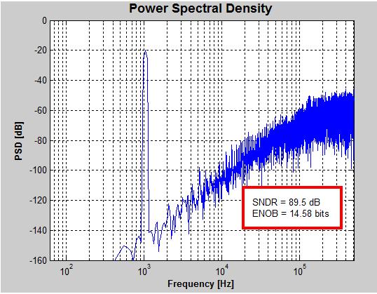
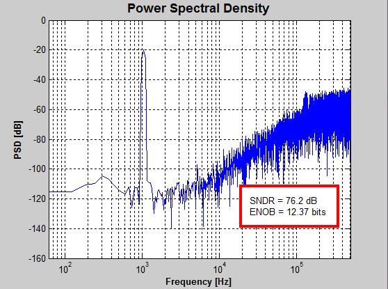
6 augmentation of the input signal frequency creates difficulty to the amplifier to restore the signal faithfully. For the amplifier responds linearly, it generally we define a maximum frequency above which the amplifier distorts the output signal. For a sinusoidal signal of amplitude A pulsation ω, this frequency is defined by GBW = 2πAf SR For a converter it is: 1 f = 2πA2 n τ f = SR 2πA T is the settling time, τ = 1/ 2πGBW and n the resolution of the converter. In the case of a switched-capacitor integrator (the main constituent of a ΣΔ modulator) the maximum speed cause an error "settling error" on the output voltage of the integrator. Indeed, the finite width of the band and "slew-rate" of the amplifier are related and may occur in the switched-capacitor circuit transient response non-ideal operation, "slew-rate" producing each clock tick an incomplete charge transfer at the end of the integration period. The effect of the finite bandwidth and the slew-rate are related to each other and may be interpreted as a non-linear gain. (13) (14) Fig. 9 SIMULINK model of second order ΣΔ modulator VI. SIMULATION RESULTS To validate the proposed model designed for various non-idealities, we perform various simulations on the SIMULINK model on the model shown in Fig.9. A minimum SNDR of 90dB is required for the low frequency biomedical applications. The simulation parameters used for simulation are summarized in Table I. Table II compares the total SNDR and the corresponding effective number of bits (ENOB) which is nothing but the maximum number of resolution can be obtained from the architecture. TABLE I SIMULATION PARAMETERS Parameter Value Signal Bandwidth BW = 4Khz Sampling frequency F s = 1.008MHz Oversampling Ratio R = 126 Sampling number N = Integrator Gain b 1 = b 2 = nd order ΣΔ Modulator Parameter TABLE II SIMULATION RESULTS SNDR [db] ENOB [bits] Ideal Sampling jitter (Δτ = 6ns) Switches ( kt/c) noise (C s = 6pF) Finite bandwidth (GBW = 8.6MHz) Slew Rate (SR = 16V/µs) Saturation Voltages (V max = ±5V) Page
 (d)")

7 (a) (b) (C) (d) 40 Page


8 (e) Fig. 10. PSD of (a) Sampling jitter Δτ = 6ns (b) Switches ( kt/c) noise C s= 6pF (c)gbw = 8.6MHz(d) Slew Rate SR = 16V/µs (e) Saturation Voltage V max = ±5V) Fig. 11.Comparison plot of the Ideal SMD and SMD with Non Idealities VII. CONCLUSION In this paper a modeling of second order sigma delta modulator is studied with various nonidealities of the modulator like operational amplifier noise, thermal noise, finite DC gain and comparison of ideal and non ideal SMD has also been done. The experimental results show that, SMD which is presented here have similarity with the ideal modulator. The performance of the second order ΣΔ modulator can be further being improved with the help of evolutionary algorithms like genetic algorithm (GA). Future work can be done with modeling of the SMD with GA. REFERENCES [1] Dragi.a Milovanović, Milan Savić, Miljan Nikolić, Second-Order Sigma-Delta Modulator in Standard CMOS Technology, SERBIAN JOURNAL OF ELECTRICAL ENGINEERING Vol. 1, No. 3, November 2004, [2] E. Janssen, A. van Roermund, Look-Ahead Based Sigma-Delta Modulation, Analog Circuits and Signal Processing, DOI / _2, Springer Science+Business Media B.V [3] Shashant Jaykar, Prachi Palsodkar, Pravin Dakhole, Modeling of Sigma-Delta Modulator Non-Idealities in MATLAB/SIMULINK, 2011 International Conference on Communication Systems and NetworkTechnologies, /11 $ IEEE DOI /CSNT [4] E. Farshidi, S. M. Sayedi, A Second-order Low Power Current- Mode Continuous-Time Sigma-Delta Modulator, ASICON'07, Proceeding of the 7th IEEE International Conference on ASIC, Guilin, China, pp , Oct [5] E. Boser and B. A. Wooley, The Design of Sigma-Delta Modulation Analog-to-Digital Converters, IEEE J. Solid- State Circ., vol. 23, pp , Dec [6] S. Brigati, F. Francesconi, P. Malcovati, D. Tonietto, A. Baschirotto and F. Maloberti, MODELING SIGMA-DELTA MODULATOR NONIDEALITIES IN SIMULINK, IEEE International Symposium, pp vol.2, [7] Abdelghani Dendouga, Nour-Eddine Bouguechal, Souhil Kouda and Samir Barra, Modeling of a Second Order Non-Ideal Sigma- Delta Modulator, International Journal of Electrical and Compute Engineering 5: [8] G. Temes, Finite amplifier gain and bandwidth effects in switched capacitor filters, IEEE J. Solid-State Circuits, vol. 15, pp , June1980. [9] H. Zare-Hoseini and I. Kale, On the effects of finite and nonlinear DCgain on the switched-capacitor delta-sigma modulators, in Proc. IEEE Int. Symp. Circuits Systems, May 2005, pp Page
9 [10] F. Medeiro et al., Modeling opamp-induced harmonic distortion for switched-capacitor SD modulator design, in IEEE Int. Symp. Circuits Systems, vol. 5, May-Jun. 1994, pp [11] Ms.R.W.Jasutkar, Dr.P.R.Baja,j Dr.A.Y.Deshmukh, GA Based Low Power Sigma Delta Modulator for Biomedical Applications, /11/$ IEEE [12] Youngcheol Chae and Gunhee Han A Low Power Sigma Delta Modulator Using Class-C Inverter in 2007 Symposium on VLSI circuits Digest of Technical Papers. [13] Shanthi Pavan, and Prabu Sankar Power Reduction in Continuous-Time Delta-Sigma Modulators Using the Assisted Opamp Technique in IEEE Journal Of Solid-State Circuits, Vol. 45, No. 7, July [14] Arnold R. Feldman, Bernhard E. Boser, and Paul R. Gray, Fellow, A 13-Bit, 1.4-MS/s Sigma Delta Modulator for RF Baseband Channel Applications in IEEE Journal Of Solid-State Circuits, Vol. 33, No. 10, October [15] M.Loulou, D.Dallet and P.Marchegay A 3.3V Switched Current Second Order Sigma Delta Modulator for Audio Applications in IEEE [16] Ebrahim Farshidi, Navid Alaei-Sheini A Micropower Current Mode Sigma Delta Modulator for Biomedical Applications in IEEE [17] Chen Yueyang, Zhong Shun an, Dang Hua Design of A low-power consumption and high-performance sigma-delta Modulator in 2009World Congress on Computer Science and Information Engineering /08 $ IEEE. [18] Guo-Ming Sung, Chih-Ping Yu, Dong-An Yao A Comparison of Second-Order Sigma-Delta Modulator Between Switched- Capacitor and Switched-Current Techniques in /08/$ IEEE. 42 Page
MASH 2-1 MULTI-BIT SIGMA-DELTA MODULATOR FOR WLAN L 2 ( ) ( ) 1( 1 1 1
 ( ) 1( 1 1 1") MASH 2- MULTI-BIT SIGMA-DELTA MODULATOR FOR WLAN Yu hang, Ning Xie, Hui Wang and Yejun He College of Information Engineering, Shenzhen University, Shenzhen, Guangdong 58060, China kensouren@yahoo.com.cn
MASH 2- MULTI-BIT SIGMA-DELTA MODULATOR FOR WLAN Yu hang, Ning Xie, Hui Wang and Yejun He College of Information Engineering, Shenzhen University, Shenzhen, Guangdong 58060, China kensouren@yahoo.com.cn
Second-Order Sigma-Delta Modulator in Standard CMOS Technology
 SERBIAN JOURNAL OF ELECTRICAL ENGINEERING Vol. 1, No. 3, November 2004, 37-44 Second-Order Sigma-Delta Modulator in Standard CMOS Technology Dragiša Milovanović 1, Milan Savić 1, Miljan Nikolić 1 Abstract:
MODELING BAND-PASS SIGMA-DELTA MODULATORS IN SIMULINK
 Vienna, AUSTRIA, 000, Septemer 5-8 MODELING BAND-PASS SIGMA-DELTA MODULATORS IN SIMULINK S. Brigati (), F. Francesconi (), P. Malcovati () and F. Maloerti (3) () Dep. of Electrical Engineering, University
Modeling of a Second Order Sigma-Delta Modulator with Imperfections
 International Journal on Electrical Engineering and Informatics - Volume 3, Number 2, 2011 International Journal on Electrical Engineering and Informatics - Volume 3, Number 2, 2011 Modeling of a Second
Design and Implementation of a Sigma Delta ADC By: Moslem Rashidi, March 2009
 Design and Implementation of a Sigma Delta ADC By: Moslem Rashidi, March 2009 Introduction The first thing in design an ADC is select architecture of ADC that is depend on parameters like bandwidth, resolution,
ECE 627 Project: Design of a High-Speed Delta-Sigma A/D Converter
 ECE 627 Project: Design of a High-Speed Delta-Sigma A/D Converter Brian L. Young youngbr@eecs.oregonstate.edu Oregon State University June 6, 28 I. INTRODUCTION The goal of the Spring 28, ECE 627 project
Oversampling Converters
 Oversampling Converters Behzad Razavi Electrical Engineering Department University of California, Los Angeles Outline Basic Concepts First- and Second-Order Loops Effect of Circuit Nonidealities Cascaded
System-Level Simulation for Continuous-Time Delta-Sigma Modulator in MATLAB SIMULINK
 Proceedings of the 5th WSEAS Int. Conf. on CIRCUITS, SYSTEMS, ELECTRONICS, CONTROL & SIGNAL PROCESSING, Dallas, USA, November 1-3, 26 236 System-Level Simulation for Continuous-Time Delta-Sigma Modulator
The Case for Oversampling
 EE47 Lecture 4 Oversampled ADCs Why oversampling? Pulse-count modulation Sigma-delta modulation 1-Bit quantization Quantization error (noise) spectrum SQNR analysis Limit cycle oscillations nd order ΣΔ
A Triple-mode Sigma-delta Modulator Design for Wireless Standards
 0th International Conference on Information Technology A Triple-mode Sigma-delta Modulator Design for Wireless Standards Babita R. Jose, P. Mythili, Jawar Singh *, Jimson Mathew * Cochin University of
Exploring of Third-Order Cascaded Multi-bit Delta- Sigma Modulator with Interstage Feedback Paths
 92 ECTI TRANSACTIONS ON ELECTRICAL ENG., ELECTRONICS, AND COMMUNICATIONS VOL.9, NO.1 February 2011 Exploring of Third-Order Cascaded Multi-bit Delta- Sigma Modulator with Interstage Feedback Paths Sarayut
Modulator with Op- Amp Gain Compensation for Nanometer CMOS Technologies
 A. Pena Perez, V.R. Gonzalez- Diaz, and F. Maloberti, ΣΔ Modulator with Op- Amp Gain Compensation for Nanometer CMOS Technologies, IEEE Proceeding of Latin American Symposium on Circuits and Systems, Feb.
CHAPTER. delta-sigma modulators 1.0
 CHAPTER 1 CHAPTER Conventional delta-sigma modulators 1.0 This Chapter presents the traditional first- and second-order DSM. The main sources for non-ideal operation are described together with some commonly
Summary Last Lecture
 Interleaved ADCs EE47 Lecture 4 Oversampled ADCs Why oversampling? Pulse-count modulation Sigma-delta modulation 1-Bit quantization Quantization error (noise) spectrum SQNR analysis Limit cycle oscillations
BandPass Sigma-Delta Modulator for wideband IF signals
 BandPass Sigma-Delta Modulator for wideband IF signals Luca Daniel (University of California, Berkeley) Marco Sabatini (STMicroelectronics Berkeley Labs) maintain the same advantages of BaseBand converters
EE247 Lecture 26. This lecture is taped on Wed. Nov. 28 th due to conflict of regular class hours with a meeting
 EE47 Lecture 6 This lecture is taped on Wed. Nov. 8 th due to conflict of regular class hours with a meeting Any questions regarding this lecture could be discussed during regular office hours or in class
A Novel Dual Mode Reconfigurable Delta Sigma Modulator for B-mode and CW Doppler Mode Operation in Ultra Sonic Applications
 A Novel Dual Mode Reconfigurable Delta Sigma Modulator for B-mode and CW Doppler Mode Operation in Ultra Sonic Applications Asghar Charmin 1, Mohammad Honarparvar 2, Esmaeil Najafi Aghdam 2 1. Department
Low Power and Fast Transient High Swing CMOS Telescopic Operational Amplifier
 RESEARCH ARTICLE OPEN ACCESS Low Power and Fast Transient High Swing CMOS Telescopic Operational Amplifier Akshay Kumar Kansal 1, Asst Prof. Gayatri Sakya 2 Electronics and Communication Department, 1,2
A VCO-based analog-to-digital converter with secondorder sigma-delta noise shaping
 A VCO-based analog-to-digital converter with secondorder sigma-delta noise shaping The MIT Faculty has made this article openly available. Please share how this access benefits you. Your story matters.
Combining Multipath and Single-Path Time-Interleaved Delta-Sigma Modulators Ahmed Gharbiya and David A. Johns
 1224 IEEE TRANSACTIONS ON CIRCUITS AND SYSTEMS II: EXPRESS BRIEFS, VOL. 55, NO. 12, DECEMBER 2008 Combining Multipath and Single-Path Time-Interleaved Delta-Sigma Modulators Ahmed Gharbiya and David A.
RELAXED TIMING ISSUE IN GLOBAL FEEDBACK PATHS OF UNITY- STF SMASH SIGMA DELTA MODULATOR ARCHITECTURE
 RELAXED TIMING ISSUE IN GLOBAL FEEDBACK PATHS OF UNITY- STF SMASH SIGMA DELTA MODULATOR ARCHITECTURE Mehdi Taghizadeh and Sirus Sadughi Department of Electrical Engineering, Science and Research Branch,
EE247 Lecture 26. EE247 Lecture 26
 EE247 Lecture 26 Administrative EE247 Final exam: Date: Mon. Dec. 18 th Time: 12:30pm-3:30pm Location: 241 Cory Hall Extra office hours: Thurs. Dec. 14 th, 10:30am-12pm Closed book/course notes No calculators/cell
Very Low Power Sigma Delta Modulator for Biomedical Applications
 IOSR Journal of VLSI and Signal Processing (IOSR-JVSP) Volume 6, Issue 1, Ver. I (Jan. -Feb. 2016), PP 01-08 e-issn: 2319 4200, p-issn No. : 2319 4197 www.iosrjournals.org Very Low Power Sigma Delta Modulator
Design of Continuous Time Multibit Sigma Delta ADC for Next Generation Wireless Applications
 RESEARCH ARTICLE OPEN ACCESS Design of Continuous Time Multibit Sigma Delta ADC for Next Generation Wireless Applications Sharon Theresa George*, J. Mangaiyarkarasi** *(Department of Information and Communication
EE247 Lecture 24. EE247 Lecture 24
 EE247 Lecture 24 Administrative EE247 Final exam: Date: Wed. Dec. 15 th Time: -12:30pm-3:30pm- Location: 289 Cory Closed book/course notes No calculators/cell phones/pdas/computers Bring one 8x11 paper
Analog-to-Digital Converters
 EE47 Lecture 3 Oversampled ADCs Why oversampling? Pulse-count modulation Sigma-delta modulation 1-Bit quantization Quantization error (noise) spectrum SQNR analysis Limit cycle oscillations nd order ΣΔ
Gábor C. Temes. School of Electrical Engineering and Computer Science Oregon State University. 1/25
 Gábor C. Temes School of Electrical Engineering and Computer Science Oregon State University temes@ece.orst.edu 1/25 Noise Intrinsic (inherent) noise: generated by random physical effects in the devices.
Outline. Noise and Distortion. Noise basics Component and system noise Distortion INF4420. Jørgen Andreas Michaelsen Spring / 45 2 / 45
 INF440 Noise and Distortion Jørgen Andreas Michaelsen Spring 013 1 / 45 Outline Noise basics Component and system noise Distortion Spring 013 Noise and distortion / 45 Introduction We have already considered
Architectures and Design Methodologies for Very Low Power and Power Effective A/D Sigma-Delta Converters
 0 Architectures and Design Methodologies for Very Low Power and Power Effective A/D Sigma-Delta Converters F. Maloberti University of Pavia - Italy franco.maloberti@unipv.it 1 Introduction Summary Sigma-Delta
DESIGN OF MULTI-BIT DELTA-SIGMA A/D CONVERTERS
 DESIGN OF MULTI-BIT DELTA-SIGMA A/D CONVERTERS DESIGN OF MULTI-BIT DELTA-SIGMA A/D CONVERTERS by Yves Geerts Alcatel Microelectronics, Belgium Michiel Steyaert KU Leuven, Belgium and Willy Sansen KU Leuven,
A new class AB folded-cascode operational amplifier
 A new class AB folded-cascode operational amplifier Mohammad Yavari a) Integrated Circuits Design Laboratory, Department of Electrical Engineering, Amirkabir University of Technology, Tehran, Iran a) myavari@aut.ac.ir
Tuesday, March 22nd, 9:15 11:00
 Nonlinearity it and mismatch Tuesday, March 22nd, 9:15 11:00 Snorre Aunet (sa@ifi.uio.no) Nanoelectronics group Department of Informatics University of Oslo Last time and today, Tuesday 22nd of March:
VIRTUAL TEST BENCH FOR DESIGN AND SIMULATION OF DATA CONVERTERS
 VIRTUAL TEST BENCH FOR DESIGN AND SIMULATION OF DATA CONVERTERS P. Est~ada, F. Malobed 1.. Texas A&M University, College Station, Texas, USA. 2. University of Pavia, Pavia, Italy and University of Texas
Lecture #6: Analog-to-Digital Converter
 Lecture #6: Analog-to-Digital Converter All electrical signals in the real world are analog, and their waveforms are continuous in time. Since most signal processing is done digitally in discrete time,
Integrated Microsystems Laboratory. Franco Maloberti
 University of Pavia Integrated Microsystems Laboratory Power Efficient Data Convertes Franco Maloberti franco.maloberti@unipv.it OUTLINE Introduction Managing the noise power budget Challenges of State-of-the-art
INF4420. ΔΣ data converters. Jørgen Andreas Michaelsen Spring 2012
 INF4420 ΔΣ data converters Spring 2012 Jørgen Andreas Michaelsen (jorgenam@ifi.uio.no) Outline Oversampling Noise shaping Circuit design issues Higher order noise shaping Introduction So far we have considered
Design of Pipeline Analog to Digital Converter
 Design of Pipeline Analog to Digital Converter Vivek Tripathi, Chandrajit Debnath, Rakesh Malik STMicroelectronics The pipeline analog-to-digital converter (ADC) architecture is the most popular topology
BANDPASS delta sigma ( ) modulators are used to digitize
 modulators are used to digitize") 680 IEEE TRANSACTIONS ON CIRCUITS AND SYSTEMS II: EXPRESS BRIEFS, VOL. 52, NO. 10, OCTOBER 2005 A Time-Delay Jitter-Insensitive Continuous-Time Bandpass 16 Modulator Architecture Anurag Pulincherry, Michael
680 IEEE TRANSACTIONS ON CIRCUITS AND SYSTEMS II: EXPRESS BRIEFS, VOL. 52, NO. 10, OCTOBER 2005 A Time-Delay Jitter-Insensitive Continuous-Time Bandpass 16 Modulator Architecture Anurag Pulincherry, Michael
A Switched-Capacitor Band-Pass Biquad Filter Using a Simple Quasi-unity Gain Amplifier
 A Switched-Capacitor Band-Pass Biquad Filter Using a Simple Quasi-unity Gain Amplifier Hugo Serra, Nuno Paulino, and João Goes Centre for Technologies and Systems (CTS) UNINOVA Dept. of Electrical Engineering
Sigma-Delta ADC Tutorial and Latest Development in 90 nm CMOS for SoC
 Sigma-Delta ADC Tutorial and Latest Development in 90 nm CMOS for SoC Jinseok Koh Wireless Analog Technology Center Texas Instruments Inc. Dallas, TX Outline Fundamentals for ADCs Over-sampling and Noise
Summary Last Lecture
 EE47 Lecture 5 Pipelined ADCs (continued) How many bits per stage? Algorithmic ADCs utilizing pipeline structure Advanced background calibration techniques Oversampled ADCs Why oversampling? Pulse-count
NPTEL. VLSI Data Conversion Circuits - Video course. Electronics & Communication Engineering.
 NPTEL Syllabus VLSI Data Conversion Circuits - Video course COURSE OUTLINE This course covers the analysis and design of CMOS Analog-to-Digital and Digital-to-Analog Converters,with about 7 design assigments.
New Features of IEEE Std Digitizing Waveform Recorders
 New Features of IEEE Std 1057-2007 Digitizing Waveform Recorders William B. Boyer 1, Thomas E. Linnenbrink 2, Jerome Blair 3, 1 Chair, Subcommittee on Digital Waveform Recorders Sandia National Laboratories
University of East London Institutional Repository:
 University of East London Institutional Repository: http://roar.uel.ac.uk This paper is made available online in accordance with publisher policies. Please scroll down to view the document itself. Please
Advanced Operational Amplifiers
 IsLab Analog Integrated Circuit Design OPA2-47 Advanced Operational Amplifiers כ Kyungpook National University IsLab Analog Integrated Circuit Design OPA2-1 Advanced Current Mirrors and Opamps Two-stage
Applied Electronics II
 Applied Electronics II Chapter 3: Operational Amplifier Part 1- Op Amp Basics School of Electrical and Computer Engineering Addis Ababa Institute of Technology Addis Ababa University Daniel D./Getachew
On the Study of Improving Noise Shaping Techniques in Wide Bandwidth Sigma Delta Modulators
 On the Study of Improving Noise Shaping Techniques in Wide Bandwidth Sigma Delta Modulators By Du Yun Master Degree in Electrical and Electronics Engineering 2013 Faculty of Science and Technology University
2.4 A/D Converter Survey Linearity
 2.4 A/D Converter Survey 21 mum and minimum power spectral density (PSD) levels. In the case of a single-channel receiver, this implies the gain control range of the VGA, while in a multi-channel receiver
Tones. EECS 247 Lecture 21: Oversampled ADC Implementation 2002 B. Boser 1. 1/512 1/16-1/64 b1. 1/10 1 1/4 1/4 1/8 k1z -1 1-z -1 I1. k2z -1.
 Tones 5 th order Σ modulator DC inputs Tones Dither kt/c noise EECS 47 Lecture : Oversampled ADC Implementation B. Boser 5 th Order Modulator /5 /6-/64 b b b b X / /4 /4 /8 kz - -z - I kz - -z - I k3z
Chapter 9: Operational Amplifiers
 Chapter 9: Operational Amplifiers The Operational Amplifier (or op-amp) is the ideal, simple amplifier. It is an integrated circuit (IC). An IC contains many discrete components (resistors, capacitors,
3 rd order Sigma-delta modulator with delayed feed-forward path for low-power applications
 3 rd order Sigma-delta modulator with delayed feed-forward path for low-power applications Min-woong Lee, Seong-ik Cho Electronic Engineering Chonbuk National University 567 Baekje-daero, deokjin-gu, Jeonju-si,
DESIGN OF LOW POWER SAR ADC FOR ECG USING 45nm CMOS TECHNOLOGY
 DESIGN OF LOW POWER SAR ADC FOR ECG USING 45nm CMOS TECHNOLOGY Silpa Kesav 1, K.S.Nayanathara 2 and B.K. Madhavi 3 1,2 (ECE, CVR College of Engineering, Hyderabad, India) 3 (ECE, Sridevi Women s Engineering
NEW CIRCUIT TECHNIQUES AND DESIGN METHODES FOR INTEGRATED CIRCUITS PROCESSING SIGNALS FROM CMOS SENSORS
 11 NEW CIRCUIT TECHNIQUES ND DESIGN METHODES FOR INTEGRTED CIRCUITS PROCESSING SIGNLS FROM CMOS SENSORS Paul ULPOIU *, Emil SOFRON ** * Texas Instruments, Dallas, US, Email: paul.vulpoiu@gmail.com ** University
Improved Modeling of Sigma- Delta Modulator Non- Idealities in SIMULINK
 A. Fornasari, P. Malcovati, F. Maloberti: "Improved Model of Sima-Delta Modulator Non-Idealities SIMULINK"; Proc. of the IEEE International Symposium on Circuits and Systems, ISCAS 005, Kobe, 3-6 May,
Chapter 2. Operational Amplifiers
 Chapter 2. Operational Amplifiers Tong In Oh 1 2.5 Integrators and Differentiators Utilized resistors in the op-amp feedback and feed-in path Ideally independent of frequency Use of capacitors together
ECEN 325 Lab 5: Operational Amplifiers Part III
 ECEN Lab : Operational Amplifiers Part III Objectives The purpose of the lab is to study some of the opamp configurations commonly found in practical applications and also investigate the non-idealities
Low-Power Pipelined ADC Design for Wireless LANs
 Low-Power Pipelined ADC Design for Wireless LANs J. Arias, D. Bisbal, J. San Pablo, L. Quintanilla, L. Enriquez, J. Vicente, J. Barbolla Dept. de Electricidad y Electrónica, E.T.S.I. de Telecomunicación,
A PSEUDO-CLASS-AB TELESCOPIC-CASCODE OPERATIONAL AMPLIFIER
 A PSEUDO-CLASS-AB TELESCOPIC-CASCODE OPERATIONAL AMPLIFIER M. Taherzadeh-Sani, R. Lotfi, and O. Shoaei ABSTRACT A novel class-ab architecture for single-stage operational amplifiers is presented. The structure
CMOS Circuit for Low Photocurrent Measurements
 CMOS Circuit for Low Photocurrent Measurements W. Guggenbühl, T. Loeliger, M. Uster, and F. Grogg Electronics Laboratory Swiss Federal Institute of Technology Zurich, Switzerland A CMOS amplifier / analog-to-digital
EE247 Lecture 22. Figures of merit (FOM) and trends for ADCs How to use/not use FOM. EECS 247 Lecture 22: Data Converters 2004 H. K.
 and trends for ADCs How to use/not use FOM. EECS 247 Lecture 22: Data Converters 2004 H. K.") EE247 Lecture 22 Pipelined ADCs Combining the bits Stage implementation Circuits Noise budgeting Figures of merit (FOM) and trends for ADCs How to use/not use FOM Oversampled ADCs EECS 247 Lecture 22:
EE247 Lecture 22 Pipelined ADCs Combining the bits Stage implementation Circuits Noise budgeting Figures of merit (FOM) and trends for ADCs How to use/not use FOM Oversampled ADCs EECS 247 Lecture 22:
UNIVERSITY OF NORTH CAROLINA AT CHARLOTTE Department of Electrical and Computer Engineering
 UNIVERSITY OF NORTH CAROLINA AT CHARLOTTE Department of Electrical and Computer Engineering EXPERIMENT 5 GAIN-BANDWIDTH PRODUCT AND SLEW RATE OBJECTIVES In this experiment the student will explore two
Design and Analysis of Two-Stage Op-Amp in 0.25µm CMOS Technology
 Design and Analysis of Two-Stage Op-Amp in 0.25µm CMOS Technology 1 SagarChetani 1, JagveerVerma 2 Department of Electronics and Tele-communication Engineering, Choukasey Engineering College, Bilaspur
Re-configurable Switched Capacitor Sigma-Delta Modulator for MEMS Microphones in Mobiles
 Re-configurable Switched Capacitor Sigma-Delta Modulator for MEMS Microphones in Mobiles M. Grassi, F. Conso, G. Rocca, P. Malcovati and A. Baschirotto Abstract This paper presents a reconfigurable discrete-time
Noise and Distortion in Microwave System
 Noise and Distortion in Microwave System Prof. Tzong-Lin Wu EMC Laboratory Department of Electrical Engineering National Taiwan University 1 Introduction Noise is a random process from many sources: thermal,
System on a Chip. Prof. Dr. Michael Kraft
 System on a Chip Prof. Dr. Michael Kraft Lecture 5: Data Conversion ADC Background/Theory Examples Background Physical systems are typically analogue To apply digital signal processing, the analogue signal
Analog CMOS Interface Circuits for UMSI Chip of Environmental Monitoring Microsystem
 Analog CMOS Interface Circuits for UMSI Chip of Environmental Monitoring Microsystem A report Submitted to Canopus Systems Inc. Zuhail Sainudeen and Navid Yazdi Arizona State University July 2001 1. Overview
Analog Circuits Prof. Jayanta Mukherjee Department of Electrical Engineering Indian Institute of Technology-Bombay
 Analog Circuits Prof. Jayanta Mukherjee Department of Electrical Engineering Indian Institute of Technology-Bombay Week -02 Module -01 Non Idealities in Op-Amp (Finite Gain, Finite Bandwidth and Slew Rate)
Pankaj Naik Electronic and Instrumentation Deptt. SGSITS, Indore, India. Priyanka Sharma Electronic and. SGSITS, Indore, India
 Designing Of Current Mode Instrumentation Amplifier For Bio-Signal Using 180nm CMOS Technology Sonu Mourya Electronic and Instrumentation Deptt. SGSITS, Indore, India Pankaj Naik Electronic and Instrumentation
A 9.35-ENOB, 14.8 fj/conv.-step Fully- Passive Noise-Shaping SAR ADC
 A 9.35-ENOB, 14.8 fj/conv.-step Fully- Passive Noise-Shaping SAR ADC Zhijie Chen, Masaya Miyahara, Akira Matsuzawa Tokyo Institute of Technology Symposia on VLSI Technology and Circuits Outline Background
Operational Amplifier as A Black Box
 Chapter 8 Operational Amplifier as A Black Box 8. General Considerations 8.2 Op-Amp-Based Circuits 8.3 Nonlinear Functions 8.4 Op-Amp Nonidealities 8.5 Design Examples Chapter Outline CH8 Operational Amplifier
DAT175: Topics in Electronic System Design
 DAT175: Topics in Electronic System Design Analog Readout Circuitry for Hearing Aid in STM90nm 21 February 2010 Remzi Yagiz Mungan v1.10 1. Introduction In this project, the aim is to design an adjustable
ELT Receiver Architectures and Signal Processing Fall Mandatory homework exercises
 ELT-44006 Receiver Architectures and Signal Processing Fall 2014 1 Mandatory homework exercises - Individual solutions to be returned to Markku Renfors by email or in paper format. - Solutions are expected
A New Current-Mode Sigma Delta Modulator
 A New Current-Mode Sigma Delta Modulator Ebrahim Farshidi 1 1 Department of Electrical Engineering, Faculty of Engineering, Shoushtar Branch, Islamic Azad university, Shoushtar, Iran e_farshidi@hotmail.com
A 2.5 V 109 db DR ADC for Audio Application
 276 JOURNAL OF SEMICONDUCTOR TECHNOLOGY AND SCIENCE, VOL.10, NO.4, DECEMBER, 2010 A 2.5 V 109 db DR ADC for Audio Application Gwangyol Noh and Gil-Cho Ahn Abstract A 2.5 V feed-forward second-order deltasigma
Analog to Digital Conversion
 Analog to Digital Conversion Florian Erdinger Lehrstuhl für Schaltungstechnik und Simulation Technische Informatik der Uni Heidelberg VLSI Design - Mixed Mode Simulation F. Erdinger, ZITI, Uni Heidelberg
Noise Lecture 1. EEL6935 Chris Dougherty (TA)
") Noise Lecture 1 EEL6935 Chris Dougherty (TA) An IEEE Definition of Noise The IEEE Standard Dictionary of Electrical and Electronics Terms defines noise (as a general term) as: unwanted disturbances superposed
Noise Lecture 1 EEL6935 Chris Dougherty (TA) An IEEE Definition of Noise The IEEE Standard Dictionary of Electrical and Electronics Terms defines noise (as a general term) as: unwanted disturbances superposed
Data Converters. Springer FRANCO MALOBERTI. Pavia University, Italy
 Data Converters by FRANCO MALOBERTI Pavia University, Italy Springer Contents Dedicat ion Preface 1. BACKGROUND ELEMENTS 1.1 1.2 1.3 1.4 1.5 1.6 1.7 1.8 The Ideal Data Converter Sampling 1.2.1 Undersampling
THE USE of multibit quantizers in oversampling analogto-digital
 966 IEEE TRANSACTIONS ON CIRCUITS AND SYSTEMS II: EXPRESS BRIEFS, VOL. 57, NO. 12, DECEMBER 2010 A New DAC Mismatch Shaping Technique for Sigma Delta Modulators Mohamed Aboudina, Member, IEEE, and Behzad
Data Conversion Techniques (DAT115)
") Data Conversion Techniques (DAT115) Hand in Report Second Order Sigma Delta Modulator with Interleaving Scheme Group 14N Remzi Yagiz Mungan, Christoffer Holmström [ 1 20 ] Contents 1. Task Description...
Data Conversion Techniques (DAT115) Hand in Report Second Order Sigma Delta Modulator with Interleaving Scheme Group 14N Remzi Yagiz Mungan, Christoffer Holmström [ 1 20 ] Contents 1. Task Description...
Time- interleaved sigma- delta modulator using output prediction scheme
 K.- S. Lee, F. Maloberti: "Time-interleaved sigma-delta modulator using output prediction scheme"; IEEE Transactions on Circuits and Systems II: Express Briefs, Vol. 51, Issue 10, Oct. 2004, pp. 537-541.
Appendix A Comparison of ADC Architectures
 Appendix A Comparison of ADC Architectures A comparison of continuous-time delta-sigma (CT ), pipeline, and timeinterleaved (TI) SAR ADCs which target wide signal bandwidths (greater than 100 MHz) and
EE247 Lecture 27. EE247 Lecture 27
 EE247 Lecture 27 Administrative EE247 Final exam: Date: Wed. Dec. 19 th Time: 12:30pm-3:30pm Location: 70 Evans Hall Extra office hours: Thurs. Dec. 13 th, 10:am2pm Closed course notes/books No calculators/cell
Lecture 2: Non-Ideal Amps and Op-Amps
 Lecture 2: Non-Ideal Amps and Op-Amps Prof. Ali M. Niknejad Department of EECS University of California, Berkeley Practical Op-Amps Linear Imperfections: Finite open-loop gain (A 0 < ) Finite input resistance
Two- Path Band- Pass Σ- Δ Modulator with 40- MHz IF 72- db DR at 1- MHz Bandwidth Consuming 16 mw
 I. Galdi, E. Bonizzoni, F. Maloberti, G. Manganaro, P. Malcovati: "Two-Path Band- Pass Σ-Δ Modulator with 40-MHz IF 72-dB DR at 1-MHz Bandwidth Consuming 16 mw"; 33rd European Solid State Circuits Conf.,
INF4420 Switched capacitor circuits Outline
 INF4420 Switched capacitor circuits Spring 2012 1 / 54 Outline Switched capacitor introduction MOSFET as an analog switch z-transform Switched capacitor integrators 2 / 54 Introduction Discrete time analog
CMOS High Speed A/D Converter Architectures
 CHAPTER 3 CMOS High Speed A/D Converter Architectures 3.1 Introduction In the previous chapter, basic key functions are examined with special emphasis on the power dissipation associated with its implementation.
Low-Voltage Low-Power Switched-Current Circuits and Systems
 Low-Voltage Low-Power Switched-Current Circuits and Systems Nianxiong Tan and Sven Eriksson Dept. of Electrical Engineering Linköping University S-581 83 Linköping, Sweden Abstract This paper presents
Low- Power Third- Order ΣΔ Modulator with Cross Couple Paths for WCDMA Applications
 C. Della Fiore, F. Maloberti, P. Malcovati: "Low-Power Third-Order ΣΔ Modulator with Cross Couple Paths for WCDMA Applications"; Ph. D. Research in Microelectronics and Electronics, PRIME 2006, Otranto,
Oversampling Data Converters Tuesday, March 15th, 9:15 11:40
 Oversampling Data Converters Tuesday, March 15th, 9:15 11:40 Snorre Aunet (sa@ifi.uio.no) Nanoelectronics group Department of Informatics University of Oslo Last time and today, Tuesday 15th of March:
Cascaded Noise Shaping for Oversampling A/D and D/A Conversion Bruce A. Wooley Stanford University
 Cascaded Noise Shaping for Oversampling A/D and D/A Conversion Bruce A. Wooley Stanford University Bruce A. Wooley - 1 - Copyright 2005, Stanford University Outline Oversampling modulators for A-to-D conversion
Fundamentals of Data Converters. DAVID KRESS Director of Technical Marketing
 Fundamentals of Data Converters DAVID KRESS Director of Technical Marketing 9/14/2016 Analog to Electronic Signal Processing Sensor (INPUT) Amp Converter Digital Processor Actuator (OUTPUT) Amp Converter
Reconfigurable Low-Power Continuous-Time Sigma-Delta Converter for Multi- Standard Applications
 ECEN-60: Mixed-Signal Interfaces Instructor: Sebastian Hoyos ASSIGNMENT 6 Reconfigurable Low-Power Continuous-Time Sigma-Delta Converter for Multi- Standard Applications ) Please use SIMULINK to design
Cascaded Noise-Shaping Modulators for Oversampled Data Conversion
 Cascaded Noise-Shaping Modulators for Oversampled Data Conversion Bruce A. Wooley Stanford University B. Wooley, Stanford, 2004 1 Outline Oversampling modulators for A/D conversion Cascaded noise-shaping
ANALYSIS AND DESIGN OF HIGH CMRR INSTRUMENTATION AMPLIFIER FOR ECG SIGNAL ACQUISITION SYSTEM USING 180nm CMOS TECHNOLOGY
 International Journal of Electronics and Communication Engineering (IJECE) ISSN 2278-9901 Vol. 2, Issue 4, Sep 2013, 67-74 IASET ANALYSIS AND DESIGN OF HIGH CMRR INSTRUMENTATION AMPLIFIER FOR ECG SIGNAL
ANALYSIS, DESIGN AND IMPLEMENTATION OF NOISE SHAPING DATA CONVERTERS FOR POWER SYSTEMS
 ANALYSIS, DESIGN AND IMPLEMENTATION OF NOISE SHAPING DATA CONVERTERS FOR POWER SYSTEMS Maraim Asif 1, Prof Pallavi Bondriya 2 1 Department of Electrical and Electronics Engineering, Technocrats institute
Comparison of Signal Attenuation of Multiple Frequencies Between Passive and Active High-Pass Filters
 Comparison of Signal Attenuation of Multiple Frequencies Between Passive and Active High-Pass Filters Aaron Batker Pritzker Harvey Mudd College 23 November 203 Abstract Differences in behavior at different
AN increasing number of video and communication applications
 1470 IEEE JOURNAL OF SOLID-STATE CIRCUITS, VOL. 32, NO. 9, SEPTEMBER 1997 A Low-Power, High-Speed, Current-Feedback Op-Amp with a Novel Class AB High Current Output Stage Jim Bales Abstract A complementary
A Multichannel Pipeline Analog-to-Digital Converter for an Integrated 3-D Ultrasound Imaging System
 1266 IEEE JOURNAL OF SOLID-STATE CIRCUITS, VOL. 38, NO. 7, JULY 2003 A Multichannel Pipeline Analog-to-Digital Converter for an Integrated 3-D Ultrasound Imaging System Kambiz Kaviani, Student Member,
Performance Improvement of Delta Sigma Modulator for Wide-Band Continuous-Time Applications
 International OPEN ACCESS Journal Of Modern Engineering Research (IJMER) Performance Improvement of Delta Sigma Modulator for Wide-Band Continuous-Time Applications Parvathy Unnikrishnan 1, Siva Kumari
Operational Amplifiers
 Questions Easy Operational Amplifiers 1. Which of the following statements are true? a. An op-amp has two inputs and three outputs b. An op-amp has one input and two outputs c. An op-amp has two inputs