Nonlinear Equalization Processor IC for Wideband Receivers and
|
|
|
- Pearl Carter
- 6 years ago
- Views:
Transcription
1 Nonlinear Equalization Processor IC for Wideband Receivers and Sensors William S. Song, Joshua I. Kramer, James R. Mann, Karen M. Gettings, Gil M. Raz, Joel I. Goodman, Benjamin A. Miller, Matthew Herman, Thomas B. Emberley, Larry L. Retherford, Albert H. Horst HPEC 2009 RESEARCH &TECHNOLOGY, INC. 23 September 2009 This work was sponsored by DARPA under Air Force Contract FA C Opinions, interpretations, conclusions and recommendations are those of the authors and are not necessarily endorsed by the United States Government. HPEC
2 Outline Introduction Nonlinear Equalization (NLEQ) applications NLEQ program objective NLEQ processor architecture VLSI NLEQ processors Performance demonstration results Summary HPEC


3 Radar High Dynamic Range Requirements for Military and Commercial Sensor Systems Radar Receiver System Example Jamming Radar Receiver System Interference + Noise Environment Jammer Target Power (db B) Noise Clutter Dynamic Range 80->100 db Small targets at or below noise level Range Radar, ELINT, SIGINT, Comm receiver systems must support high dynamic range operation To detect small targets/signals in interference/clutter environment High signal-to-noise ratio and linearity required HPEC
4 Linearity Concerns in Highly Digitized Arrays and Frequency Channelized Systems Digital Sensor Array Receiver Receiver ADC ADC Receiver e ADC Receiver Receiver ADC ADC Receiver Receiver ADC ADC Receiver ADC Digital beamforming and frequency channelization increase in-band signal-tonoise ratio (SNR) Non-linearity generated spurs and intermods can interfere with small signal detection Power Two-tone input Noise Power Two-tone input Noise Power Two-tone input Intermods Intermods Intermods Noise Frequency Frequency Frequency HPEC Receiver ADC Frequency Channelizer Frequency Channelized Receiver Power Signal In-Band Noise Out-of-Band Noise Frequency F Nyquist
5 Nonlinear Equalization (NLEQ) From Antennas LNA Digital Receiver Digital Receiver 1 Rec Sources of Nonlinearities A/D N Digital Signal Processor HPEC
6 Nonlinear Equalization (NLEQ) Digital Receiver N Digital Receiver 1 Rec A/D LNA Digital Signal Processor Sources of Nonlinearities r (db) Power Before Equalization In-Band Intermodulation Distortions Frequency (bin) HPEC
 Before Equalization In-Band Intermodulation Distortions Power (db) Dynamic range improvement After Equalization Frequency (bin) Frequency (bin) HPEC 2009-7")
7 Nonlinear Equalization (NLEQ) Digital Receiver N From Antennas LNA Digital Receiver 1 Rec A/D Nonlinear Equalizer Digital Signal Digital Processor Signal Processor Sources of Nonlinearities Inverts Nonlinearities Power (db) Before Equalization In-Band Intermodulation Distortions Power (db) Dynamic range improvement After Equalization Frequency (bin) Frequency (bin) HPEC
8 Nonlinear Equalization (NLEQ) From Antennas Power (db) LNA Digital Receiver Digital Receiver 1 Rec Sources of Nonlinearities A/D N Before Equalization In-Band Intermodulation Distortions Nonlinear Equalizer Digital Signal Processor Inverts Nonlinearities Power (db) Dynamic range improvement Digital Signal Digital Processor Signal Processor After Equalization +20~25 db BW >1 Teraops < 2 Watts Frequency (bin) Frequency (bin) Nonlinear equalizer processor can reduce nonlinear distortion levels in analog and mixed signal circuitry Equivalent to having devices years ahead of their time HPEC
9 Outline Introduction NLEQ processor architecture Processor architecture Architecture optimization VLSI NLEQ processors Performance demonstration results Summary HPEC
10 NLEQ Polynomial Nonlinear Filter Architecture Pass-through Z -α Pass-through Σ Processing Elements Z -β β Z -β Z -β Z -β FIR X FIR FIR Z -γ 1 FIR Z -γγ 1 Z -γ 1 X X X Σ Parameters to optimize: Number of processing elements Polynomial orders of processing elements Number of taps Delay values Z -γ Ν Z -γ Ν Z Z -γ Ν Z -γ 1 Z -γ Ν HPEC


11 Wideband NLEQ Processor Parameter Optimization Z -α Pass-through Z -β FIR X Z -γ 1 Z Z -γ -γ Ν Ν HPEC Parameter selection 10 filters, 10 taps, 0-3 tap delay, 0-3 group delay, 3 pass through delay
 Design Feedback (Performance Trades) Sub-processor Task Distribution & Sizing P P P P P P P P P P P P FIR1φ1")
 IC Architecture and Floor Plan Clocks I/O FIR1φ1 FIR1φN NLP1φ1 NLP1φN FIR1φ2 FIR2φN NLP2φ1 NLP2φN Buses FIRmφ1 FIRmφN NLPmφ1 NLPmφN")
12 Parallel NLEQ Processor Architecture Optimization Distributed Polyphase Block- Floating-Point Residue Arithmetic Architecture Low V T Dynamic Logic IC Layout Distribute P P P P P P P P P P P P P P P P Reassemble e Design Feedback (Performance Trades) Design Feedback (Performance Trades) Sub-processor Task Distribution & Sizing P P P P P P P P P P P P FIR1φ1 FIR1φ2 FIR1φ3 P P P P P P P P P P P P P P P P P P P P P P P P NLP1φ1 NLP1φ2 NLP1φ3 P P P P P P P P P P P P P P P P P P P P P P P P FIR2φ1 P P P P FIR2φ2 P P P P FIR2φ3 P P P P HPEC Design Feedback (Routing Efficiency) IC Architecture and Floor Plan Clocks I/O FIR1φ1 FIR1φN NLP1φ1 NLP1φN FIR1φ2 FIR2φN NLP2φ1 NLP2φN Buses FIRmφ1 FIRmφN NLPmφ1 NLPmφN Memory Control
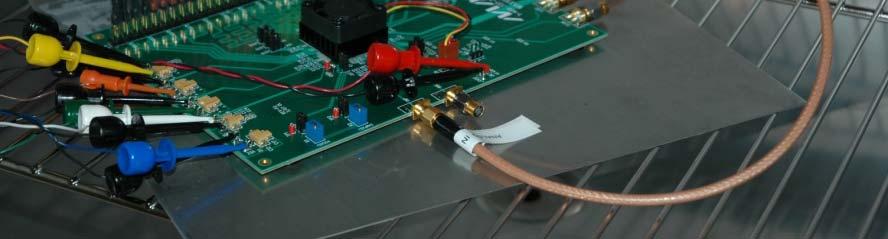
 intermods Harmonics Pow wer (dbfs) Non-tonal signal experiment parameters Amplifier in")

13 Measured Results: PRN Signal with Amplifier & ADC Distortions Unequalized In-band Typical Response Equalized Pow wer (dbfs) intermods Harmonics Pow wer (dbfs) Non-tonal signal experiment parameters Amplifier in saturation region Max 104 included d in testbed tb system Pseudo-Random Noise (band-limited) input waveform Greater than 25 db dynamic range improvement In-band signal component is not distorted by the equalizer HPEC
14 db ement uction (db) in ur Redudu FDR Improve Spu IF NLEQ Adaptive Equalization Performance Adaptive Equalization Performance Fully Adaptive Partially Adaptive Non-Adaptive Minimal performance losses uses computationally efficient i adaptive algorithm -24 Nominal training temperature Ambient Temperature Ambient Temperature in Degrees ( o C) Celcius Characterized Max 108 device sensitivity to changes in temperature Applied adaptive equalizations Fully temperature adaptive approach achieve good performance Partially adaptive approach can achieve similar performance with much higher computational efficiency HPEC
15 Outline Introduction NLEQ processor architecture VLSI NLEQ processors Enabling technologies NLEQ4000 ultra-wideband processor IC NLEQ500 wideband processor IC Performance demonstration results Summary HPEC
 Y(n) H J NLEQ Signal Processor IC IC Architecture Clocks I/O FIR1φ1 FIR1φNNLP1φ1NLP1φN FIR1φ2 FIR2φNNLP2φ1NLP2φN Buses FIRmφ1")
16 Nonlinear Equalizer Processor IC Development Process Non-Linear Equalizer Algorithm/Architecture Distributed Polyphase Residue Arithmetic Distribution P P P P P P P P P P P P P P P P Reassemble EQ FIR Partition FIR #1 Partition FIR #2 Partition FIR #N H 1 H 2 + X(n) Y(n) H J NLEQ Signal Processor IC IC Architecture Clocks I/O FIR1φ1 FIR1φNNLP1φ1NLP1φN FIR1φ2 FIR2φNNLP2φ1NLP2φN Buses FIRmφ1 FIRmφNNLPmφ1NLPmφN Memory Control Architecture Optimization Level of Pipeline Optimal Degree Region of Polyphasi ng Throughput Density Power Efficiency Throughput Density Times Power Efficiency Power (db) 1.5 Tearops 1.2 Watts 500 MHz BW MAX108 Before NLEQ After NLEQ Low Vt Dynamic Logic HPEC Frequency Bin
 Small design team (<10) HPEC")
17 Architectural Comparison of Pentium 4 and MIT LL Processor Dies Pentium 4 Die MIT LL Processor Die Processor Array Single processor 1000 s of parallel processors Multiple caches and memory bus Local memory only Only core runs at high speed Entire die runs at high speed General purpose processing Signal processing functions Large design team (>100) Small design team (<10) HPEC
18 Custom CMOS Circuit Design Standard Cell Full Adder Full Custom Full Adder Pre-designed logic gates only Automatic device placement and routing Large area and power consumption Custom logic and devices sizing Manual device placement and interconnect Small area and power consumption HPEC
19 Full Custom Low Threshold Voltage (V T ) Dynamic Logic Circuits Standard Cell Static Register Full Custom Dynamic Register Low V T Devices P = ½CV 2 f Charge Leakage Design Techniques Frequent refresh Bypass capacitors Signal isolation Guard rings Robust circuits Logic based computation and storage Many devices Charge based computation and storage Fewer devices Large area and power consumption Small area and power consumption HPEC


20 NLEQ4000 Processor IC Wideband NLEQ Processor IC Layout And BGA Package Up to 4,000MSPS Selectable bit widths Up to 12 bits input Up to 16 bits output LVDS and CMOS I/O Programmable coefficients Block floating point residue arithmetic Parameter (IBM 0.13um) Die Size Core 2.6 mm x 3.3 mm 266mW 706mW Chip 6mm x 6mm 453mW 1219mW HPEC


 Power @500MSPS (Vdd=1.")
21 NLEQ500 Processor IBM 0.13µm Die BGA Up to 500MSPS Selectable bit widths Up to 18 bits input Up to 22 bits output Low voltage CMOS I/O Programmable configuration and coefficients Block floating point residue arithmetic Yield 14/15 for LowVt and 14/15 for RegVt Parameter Core I/O Chip (IBM CMOS 0.13um) Size 0.65mm x 1.4mm N/A 2.2mm x 2.2mm 6mW 19mW* 25mW* (Vdd=0.6V) (Vdd=1.2V) 122mW 121mW* 243mW* HPEC *With 50 Ohm Load Termination
22 Outline Introduction NLEQ processor architecture VLSI NLEQ processors Performance demonstration results S Summary HPEC


23 MAX108 Demonstration Results MAX108 ADC with NLEQ4000 Without NLEQ4000 NLEQ4000 MAX108 With NLEQ4000 ~21 db linearity improvement demonstrated with NLEQ4000 IC at 1.5GSPS HPEC


24 Measured NLEQ Performance Improvement for Other ADCs Interleaving Architecture ~1 GHz Improved ~17 db Folding Architecture 1.5 GHz Improved ~13 db Flash Architecture ~1.3 GHz Improved ~12 db National Atmel AT84AS008 Entire Receiver Chain 30 MHz BW Improved ~12 db HPEC Maxim 109 LTC 2209


25 X-Band Receiver-on-Chip (RoC) Development Based on NLEQ DSP BPF LO BPF MAX108 Top View ADC NLEQ RoC Bottom View ADC LNA Mixer IF Amp Integrated RoC Die 360mW Linear dynamic range limited by the final IF amplifier NLEQ DSP to linearize the amplifier and ADC High performance and low power achieved with new analog/digital co-design paradigm Single die receiver implementation being explored NLEQ HPEC
26 Summary Linearity enhancement required by DoD/commercial sensor/receiver applications Phased array sensors/receivers Frequency channelized sensors/receivers MIT LL has developed high-throughput low-power nonlinear equalization signal processor ICs Massively yparallel systolic architecture Polyphase distributed arithmetic processing Block floating point residue number arithmetic Full custom low-threshold-voltage dynamic logic Successful demonstration results >20 db linearity improvement NLEQ4000 Up to 4GSPS, <1.25W Up to 12 bit ADCs NLEQ500 Up to 500MSPS, <0.25W Up to 18bit ADCs HPEC
Analog and RF circuit techniques in nanometer CMOS
 Analog and RF circuit techniques in nanometer CMOS Bram Nauta University of Twente The Netherlands http://icd.ewi.utwente.nl b.nauta@utwente.nl UNIVERSITY OF TWENTE. Outline Introduction Balun-LNA-Mixer
Maximizing GSPS ADC SFDR Performance: Sources of Spurs and Methods of Mitigation
 Maximizing GSPS ADC SFDR Performance: Sources of Spurs and Methods of Mitigation Marjorie Plisch Applications Engineer, Signal Path Solutions November 2012 1 Outline Overview of the issue Sources of spurs
Option 1: A programmable Digital (FIR) Filter
 Filter") Design Project Your design project is basically a module filter. A filter is basically a weighted sum of signals. The signals (input) may be related, e.g. a delayed versions of each other in time, e.g.
Design Project Your design project is basically a module filter. A filter is basically a weighted sum of signals. The signals (input) may be related, e.g. a delayed versions of each other in time, e.g.
Analog-to-Digital Converter Survey & Analysis. Bob Walden. (310) Update: July 16,1999
 Update: July 16,1999") Analog-to-Digital Converter Survey & Analysis Update: July 16,1999 References: 1. R.H. Walden, Analog-to-digital converter survey and analysis, IEEE Journal on Selected Areas in Communications, vol. 17,
Analog-to-Digital Converter Survey & Analysis Update: July 16,1999 References: 1. R.H. Walden, Analog-to-digital converter survey and analysis, IEEE Journal on Selected Areas in Communications, vol. 17,
MIT Wireless Gigabit Local Area Network WiGLAN
 MIT Wireless Gigabit Local Area Network WiGLAN Charles G. Sodini Department of Electrical Engineering and Computer Science Room 39-527 Phone (617) 253-4938 E-Mail: sodini@mit.edu Sponsors: MARCO, SRC,
A 130mW 100MS/s Pipelined ADC with 69dB SNDR Enabled by Digital Harmonic Distortion Correction. Andrea Panigada, Ian Galton
 A 130mW 100MS/s Pipelined ADC with 69dB SNDR Enabled by Digital Harmonic Distortion Correction Andrea Panigada, Ian Galton University of California at San Diego, La Jolla, CA INTEGRATED SIGNAL PROCESSING
IMPLEMENTING THE 10-BIT, 50MS/SEC PIPELINED ADC
 98 CHAPTER 5 IMPLEMENTING THE 0-BIT, 50MS/SEC PIPELINED ADC 99 5.0 INTRODUCTION This chapter is devoted to describe the implementation of a 0-bit, 50MS/sec pipelined ADC with different stage resolutions
CMOS Analog to Digital Converters : State-of-the-Art and Perspectives in Digital Communications ADC
 CMOS Analog to Digital Converters : State-of-the-Art and Perspectives in Digital Communications ADC Hussein Fakhoury and Hervé Petit C²S Research Group Presentation Outline Introduction Basic concepts
UWB Hardware Issues, Trends, Challenges, and Successes
 UWB Hardware Issues, Trends, Challenges, and Successes Larry Larson larson@ece.ucsd.edu Center for Wireless Communications 1 UWB Motivation Ultra-Wideband Large bandwidth (3.1GHz-1.6GHz) Power spectrum
FUNDAMENTALS OF ANALOG TO DIGITAL CONVERTERS: PART I.1
 FUNDAMENTALS OF ANALOG TO DIGITAL CONVERTERS: PART I.1 Many of these slides were provided by Dr. Sebastian Hoyos January 2019 Texas A&M University 1 Spring, 2019 Outline Fundamentals of Analog-to-Digital
Architectures and Design Methodologies for Very Low Power and Power Effective A/D Sigma-Delta Converters
 0 Architectures and Design Methodologies for Very Low Power and Power Effective A/D Sigma-Delta Converters F. Maloberti University of Pavia - Italy franco.maloberti@unipv.it 1 Introduction Summary Sigma-Delta
ISSCC 2004 / SESSION 25 / HIGH-RESOLUTION NYQUIST ADCs / 25.4
 ISSCC 2004 / SESSION 25 / HIGH-RESOLUTION NYQUIST ADCs / 25.4 25.4 A 1.8V 14b 10MS/s Pipelined ADC in 0.18µm CMOS with 99dB SFDR Yun Chiu, Paul R. Gray, Borivoje Nikolic University of California, Berkeley,
An All CMOS, 2.4 GHz, Fully Adaptive, Scalable, Frequency Hopped Transceiver
 An All CMOS, 2.4 GHz, Fully Adaptive, Scalable, Frequency Hopped Transceiver Farbod Behbahani John Leete Alexandre Kral Shahrzad Tadjpour Karapet Khanoyan Paul J. Chang Hooman Darabi Maryam Rofougaran
DIGITALLY ASSISTED ANALOG: REDUCING DESIGN CONSTRAINTS USING NONLINEAR DIGITAL SIGNAL PROCESSING
 DIGITALLY ASSISTED ANALOG: REDUCING DESIGN CONSTRAINTS USING NONLINEAR DIGITAL SIGNAL PROCESSING Batruni, Roy (Optichron, Inc., Fremont, CA USA, roy.batruni@optichron.com); Ramachandran, Ravi (Optichron,
APPLICATION NOTE 3942 Optimize the Buffer Amplifier/ADC Connection
 Maxim > Design Support > Technical Documents > Application Notes > Communications Circuits > APP 3942 Maxim > Design Support > Technical Documents > Application Notes > High-Speed Interconnect > APP 3942
Copyright 2007 Year IEEE. Reprinted from ISCAS 2007 International Symposium on Circuits and Systems, May This material is posted here
 Copyright 2007 Year IEEE. Reprinted from ISCAS 2007 International Symposium on Circuits and Systems, 27-30 May 2007. This material is posted here with permission of the IEEE. Such permission of the IEEE
Digital Receiver Experiment or Reality. Harry Schultz AOC Aardvark Roost Conference Pretoria 13 November 2008
 Digital Receiver Experiment or Reality Harry Schultz AOC Aardvark Roost Conference Pretoria 13 November 2008 Contents Definition of a Digital Receiver. Advantages of using digital receiver techniques.
Receiver Architecture
 Receiver Architecture Receiver basics Channel selection why not at RF? BPF first or LNA first? Direct digitization of RF signal Receiver architectures Sub-sampling receiver noise problem Heterodyne receiver
Low-Noise Amplifiers
 007/Oct 4, 31 1 General Considerations Noise Figure Low-Noise Amplifiers Table 6.1 Typical LNA characteristics in heterodyne systems. NF IIP 3 db 10 dbm Gain 15 db Input and Output Impedance 50 Ω Input
Low-Power Digital CMOS Design: A Survey
 Low-Power Digital CMOS Design: A Survey Krister Landernäs June 4, 2005 Department of Computer Science and Electronics, Mälardalen University Abstract The aim of this document is to provide the reader with
A Low Power 900MHz Superheterodyne Compressive Sensing Receiver for Sparse Frequency Signal Detection
 A Low Power 900MHz Superheterodyne Compressive Sensing Receiver for Sparse Frequency Signal Detection Hamid Nejati and Mahmood Barangi 4/14/2010 Outline Introduction System level block diagram Compressive
12-bit 50/100/125 MSPS 1-channel ADC
 SPECIFICATION 1 FEATURES TSMC CMOS 65 nm High speed pipelined ADC Resolution 12 bit Conversion rate 50/100/125 MHz Different power supplies for digital (1.2 V) and analog (1.2 V) parts Low standby current
EE247 Lecture 23. Advanced calibration techniques. Compensating inter-stage amplifier non-linearity Calibration via parallel & slow ADC
 EE247 Lecture 23 Pipelined ADCs Combining the bits Stage implementation Circuits Noise budgeting Advanced calibration techniques Compensating inter-stage amplifier non-linearity Calibration via parallel
Full Duplex Radios. Sachin Katti Kumu Networks & Stanford University 4/17/2014 1
 Full Duplex Radios Sachin Katti Kumu Networks & Stanford University 4/17/2014 1 It is generally not possible for radios to receive and transmit on the same frequency band because of the interference that
Low-Power CMOS VLSI Design
 Low-Power CMOS VLSI Design ( 范倫達 ), Ph. D. Department of Computer Science, National Chiao Tung University, Taiwan, R.O.C. Fall, 2017 ldvan@cs.nctu.edu.tw http://www.cs.nctu.tw/~ldvan/ Outline Introduction
Architectures and circuits for timeinterleaved. Sandeep Gupta Teranetics, Santa Clara, CA
 Architectures and circuits for timeinterleaved ADC s Sandeep Gupta Teranetics, Santa Clara, CA Outline Introduction to time-interleaved architectures. Conventional Sampling architectures and their application
Design and Implementation of a Sigma Delta ADC By: Moslem Rashidi, March 2009
 Design and Implementation of a Sigma Delta ADC By: Moslem Rashidi, March 2009 Introduction The first thing in design an ADC is select architecture of ADC that is depend on parameters like bandwidth, resolution,
Research and Development Activities in RF and Analog IC Design. RFIC Building Blocks. Single-Chip Transceiver Systems (I) Howard Luong
 Howard Luong") Research and Development Activities in RF and Analog IC Design Howard Luong Analog Research Laboratory Department of Electrical and Electronic Engineering Hong Kong University of Science and Technology
Research and Development Activities in RF and Analog IC Design Howard Luong Analog Research Laboratory Department of Electrical and Electronic Engineering Hong Kong University of Science and Technology
Probabilistic and Variation- Tolerant Design: Key to Continued Moore's Law. Tanay Karnik, Shekhar Borkar, Vivek De Circuit Research, Intel Labs
 Probabilistic and Variation- Tolerant Design: Key to Continued Moore's Law Tanay Karnik, Shekhar Borkar, Vivek De Circuit Research, Intel Labs 1 Outline Variations Process, supply voltage, and temperature
Implementation of Pixel Array Bezel-Less Cmos Fingerprint Sensor
 Article DOI: 10.21307/ijssis-2018-013 Issue 0 Vol. 0 Implementation of 144 64 Pixel Array Bezel-Less Cmos Fingerprint Sensor Seungmin Jung School of Information and Technology, Hanshin University, 137
Design of Pipeline Analog to Digital Converter
 Design of Pipeline Analog to Digital Converter Vivek Tripathi, Chandrajit Debnath, Rakesh Malik STMicroelectronics The pipeline analog-to-digital converter (ADC) architecture is the most popular topology
Signal Integrity Design of TSV-Based 3D IC
 Signal Integrity Design of TSV-Based 3D IC October 24, 21 Joungho Kim at KAIST joungho@ee.kaist.ac.kr http://tera.kaist.ac.kr 1 Contents 1) Driving Forces of TSV based 3D IC 2) Signal Integrity Issues
CMOS 2.4GHZ ZIGBEE/ISM TRANSMIT/RECEIVE RFeIC
 CMOS 2.4GHZ ZIGBEE/ISM TRANSMIT/RECEIVE RFeIC Description 17 1 2 3 4 TXRX VDD VDD D 16 15 14 13 12 11 10 ANT 9 The is a fully integrated, single-chip, single-die RFeIC (RF Front-end Integrated Circuit)
A/D Conversion and Filtering for Ultra Low Power Radios. Dejan Radjen Yasser Sherazi. Advanced Digital IC Design. Contents. Why is this important?
 1 Advanced Digital IC Design A/D Conversion and Filtering for Ultra Low Power Radios Dejan Radjen Yasser Sherazi Contents A/D Conversion A/D Converters Introduction ΔΣ modulator for Ultra Low Power Radios
DIGITAL INTEGRATED CIRCUITS A DESIGN PERSPECTIVE 2 N D E D I T I O N
 DIGITAL INTEGRATED CIRCUITS A DESIGN PERSPECTIVE 2 N D E D I T I O N Jan M. Rabaey, Anantha Chandrakasan, and Borivoje Nikolic CONTENTS PART I: THE FABRICS Chapter 1: Introduction (32 pages) 1.1 A Historical
Integrated receivers for mid-band SKA. Suzy Jackson Engineer, Australia Telescope National Facility
 Integrated receivers for mid-band SKA Suzy Jackson Engineer, Australia Telescope National Facility SKADS FP6 Meeting Chateau de Limelette 4-6 November, 2009 Talk overview Mid band SKA receiver challenges
AD9772A - Functional Block Diagram
 F FEATURES single 3.0 V to 3.6 V supply 14-Bit DAC Resolution 160 MPS Input Data Rate 67.5 MHz Reconstruction Passband @ 160 MPS 74 dbc FDR @ 25 MHz 2 Interpolation Filter with High- or Low-Pass Response
High-Linearity CMOS. RF Front-End Circuits
 High-Linearity CMOS RF Front-End Circuits Yongwang Ding Ramesh Harjani iigh-linearity CMOS tf Front-End Circuits - Springer Library of Congress Cataloging-in-Publication Data A C.I.P. Catalogue record
Outline. Noise and Distortion. Noise basics Component and system noise Distortion INF4420. Jørgen Andreas Michaelsen Spring / 45 2 / 45
 INF440 Noise and Distortion Jørgen Andreas Michaelsen Spring 013 1 / 45 Outline Noise basics Component and system noise Distortion Spring 013 Noise and distortion / 45 Introduction We have already considered
SPIRO SOLUTIONS PVT LTD
 VLSI S.NO PROJECT CODE TITLE YEAR ANALOG AMS(TANNER EDA) 01 ITVL01 20-Mb/s GFSK Modulator Based on 3.6-GHz Hybrid PLL With 3-b DCO Nonlinearity Calibration and Independent Delay Mismatch Control 02 ITVL02
Low Power Design for Systems on a Chip. Tutorial Outline
 Low Power Design for Systems on a Chip Mary Jane Irwin Dept of CSE Penn State University (www.cse.psu.edu/~mji) Low Power Design for SoCs ASIC Tutorial Intro.1 Tutorial Outline Introduction and motivation
Power Spring /7/05 L11 Power 1
 Power 6.884 Spring 2005 3/7/05 L11 Power 1 Lab 2 Results Pareto-Optimal Points 6.884 Spring 2005 3/7/05 L11 Power 2 Standard Projects Two basic design projects Processor variants (based on lab1&2 testrigs)
Mitigation of Nonlinear Spurious Products using Least Mean-Square (LMS)
") Mitigation of Nonlinear Spurious Products using Least Mean-Square (LMS) Nicholas Peccarelli & Caleb Fulton Advanced Radar Research Center University of Oklahoma Norman, Oklahoma, USA, 73019 Email: peccarelli@ou.edu,
Mitigation of Nonlinear Spurious Products using Least Mean-Square (LMS) Nicholas Peccarelli & Caleb Fulton Advanced Radar Research Center University of Oklahoma Norman, Oklahoma, USA, 73019 Email: peccarelli@ou.edu,
Frequency Domain UWB Multi-carrier Receiver
 Frequency Domain UWB Multi-carrier Receiver Long Bu, Joanne DeGroat, Steve Bibyk Electrical & Computer Engineering Ohio State University Research Purpose Explore UWB multi-carrier receiver architectures
A 10 bit, 1.8 GS/s Time Interleaved Pipeline ADC
 A 10 bit, 1.8 GS/s Time Interleaved Pipeline ADC M. Åberg 2, A. Rantala 2, V. Hakkarainen 1, M. Aho 1, J. Riikonen 1, D. Gomes Martin 2, K. Halonen 1 1 Electronic Circuit Design Laboratory Helsinki University
22. VLSI in Communications
 22. VLSI in Communications State-of-the-art RF Design, Communications and DSP Algorithms Design VLSI Design Isolated goals results in: - higher implementation costs - long transition time between system
Low-Power RF Integrated Circuit Design Techniques for Short-Range Wireless Connectivity
 Low-Power RF Integrated Circuit Design Techniques for Short-Range Wireless Connectivity Marvin Onabajo Assistant Professor Analog and Mixed-Signal Integrated Circuits (AMSIC) Research Laboratory Dept.
DESIGN OF A 500MHZ, 4-BIT LOW POWER ADC FOR UWB APPLICATION
 DESIGN OF A 500MHZ, 4-BIT LOW POWER ADC FOR UWB APPLICATION SANTOSH KUMAR PATNAIK 1, DR. SWAPNA BANERJEE 2 1,2 E & ECE Department, Indian Institute of Technology, Kharagpur, Kharagpur, India Abstract-This
SP 22.3: A 12mW Wide Dynamic Range CMOS Front-End for a Portable GPS Receiver
 SP 22.3: A 12mW Wide Dynamic Range CMOS Front-End for a Portable GPS Receiver Arvin R. Shahani, Derek K. Shaeffer, Thomas H. Lee Stanford University, Stanford, CA At submicron channel lengths, CMOS is
EE247 Lecture 23. EECS 247 Lecture 23 Pipelined ADCs 2008 H.K. Page 1. Pipeline ADC Block Diagram DAC ADC. V res2. Stage 2 B 2.
 EE247 Lecture 23 Pipelined ADCs (continued) Effect gain stage, sub-dac non-idealities on overall ADC performance Digital calibration (continued) Correction for inter-stage gain nonlinearity Implementation
2.4 A/D Converter Survey Linearity
 2.4 A/D Converter Survey 21 mum and minimum power spectral density (PSD) levels. In the case of a single-channel receiver, this implies the gain control range of the VGA, while in a multi-channel receiver
Course Outcome of M.Tech (VLSI Design)
") Course Outcome of M.Tech (VLSI Design) PVL108: Device Physics and Technology The students are able to: 1. Understand the basic physics of semiconductor devices and the basics theory of PN junction. 2.
Course Outcome of M.Tech (VLSI Design) PVL108: Device Physics and Technology The students are able to: 1. Understand the basic physics of semiconductor devices and the basics theory of PN junction. 2.
Scalable Front-End Digital Signal Processing for a Phased Array Radar Demonstrator. International Radar Symposium 2012 Warsaw, 24 May 2012
 Scalable Front-End Digital Signal Processing for a Phased Array Radar Demonstrator F. Winterstein, G. Sessler, M. Montagna, M. Mendijur, G. Dauron, PM. Besso International Radar Symposium 2012 Warsaw,
CMOS 2.4GHZ ZIGBEE/ISM TRANSMIT/RECEIVE RFeIC
 CMOS 2.4GHZ ZIGBEE/ISM TRANSMIT/RECEIVE RFeIC Description 17 1 2 3 4 TXRX VDD VDD D 16 15 14 13 12 11 10 ANT 9 The RFX2401C is a fully integrated, single-chip, single-die RFeIC (RF Front-end Integrated
A 1.7-to-2.2GHz Full-Duplex Transceiver System with >50dB Self-Interference Cancellation over 42MHz Bandwidth
 A 1.7-to-2.2GHz Full-Duplex Transceiver System with >50dB Self-Interference Cancellation Tong Zhang, Ali Najafi, Chenxin Su, Jacques C. Rudell University of Washington, Seattle Feb. 8, 2017 International
Cascaded Noise-Shaping Modulators for Oversampled Data Conversion
 Cascaded Noise-Shaping Modulators for Oversampled Data Conversion Bruce A. Wooley Stanford University B. Wooley, Stanford, 2004 1 Outline Oversampling modulators for A/D conversion Cascaded noise-shaping
A VCO-based analog-to-digital converter with secondorder sigma-delta noise shaping
 A VCO-based analog-to-digital converter with secondorder sigma-delta noise shaping The MIT Faculty has made this article openly available. Please share how this access benefits you. Your story matters.
A CMOS Analog Front-End for Driving a High-Speed SAR ADC in Low-Power Ultrasound Imaging Systems
 A CMOS Analog Front-End for Driving a High-Speed SAR ADC in Low-Power Ultrasound Imaging Systems Taehoon Kim, Han Yang, Sangmin Shin, Hyongmin Lee and Suhwan Kim Electrical and Computer Engineering and
Session 3. CMOS RF IC Design Principles
 Session 3 CMOS RF IC Design Principles Session Delivered by: D. Varun 1 Session Topics Standards RF wireless communications Multi standard RF transceivers RF front end architectures Frequency down conversion
2002 IEEE International Solid-State Circuits Conference 2002 IEEE
 Outline 802.11a Overview Medium Access Control Design Baseband Transmitter Design Baseband Receiver Design Chip Details What is 802.11a? IEEE standard approved in September, 1999 12 20MHz channels at 5.15-5.35
10-Bit, 40 MSPS/60 MSPS A/D Converter AD9050 REV. B. Figure 1. Typical Connections FUNCTIONAL BLOCK DIAGRAM
 a FEATURES Low Power: 1 mw @ 0 MSPS, mw @ 0 MSPS On-Chip T/H, Reference Single + V Power Supply Operation Selectable V or V Logic I/O SNR: db Minimum at MHz w/0 MSPS APPLICATIONS Medical Imaging Instrumentation
International Journal of Scientific & Engineering Research, Volume 4, Issue 5, May ISSN
 International Journal of Scientific & Engineering Research, Volume 4, Issue 5, May-2013 2190 Biquad Infinite Impulse Response Filter Using High Efficiency Charge Recovery Logic K.Surya 1, K.Chinnusamy
Digital Logic, Algorithms, and Functions for the CEBAF Upgrade LLRF System Hai Dong, Curt Hovater, John Musson, and Tomasz Plawski
 Digital Logic, Algorithms, and Functions for the CEBAF Upgrade LLRF System Hai Dong, Curt Hovater, John Musson, and Tomasz Plawski Introduction: The CEBAF upgrade Low Level Radio Frequency (LLRF) control
Hot Topics and Cool Ideas in Scaled CMOS Analog Design
 Engineering Insights 2006 Hot Topics and Cool Ideas in Scaled CMOS Analog Design C. Patrick Yue ECE, UCSB October 27, 2006 Slide 1 Our Research Focus High-speed analog and RF circuits Device modeling,
Short Range UWB Radio Systems. Finding the power/area limits of
 Short Range UWB Radio Systems Finding the power/area limits of CMOS Bob Brodersen Ian O Donnell Mike Chen Stanley Wang Integrated Impulse Transceiver RF Front-End LNA Pulser Amp Analog CLK GEN PMF Digital
Proposing. An Interpolated Pipeline ADC
 Proposing An Interpolated Pipeline ADC Akira Matsuzawa Tokyo Institute of Technology, Japan Matsuzawa & Okada Lab. Background 38GHz long range mm-wave system Role of long range mm-wave Current Optical
Antenna Measurements using Modulated Signals
 Antenna Measurements using Modulated Signals Roger Dygert MI Technologies, 1125 Satellite Boulevard, Suite 100 Suwanee, GA 30024-4629 Abstract Antenna test engineers are faced with testing increasingly
65-GHz Receiver in SiGe BiCMOS Using Monolithic Inductors and Transformers
 65-GHz Receiver in SiGe BiCMOS Using Monolithic Inductors and Transformers Michael Gordon, Terry Yao, Sorin P. Voinigescu University of Toronto March 10 2006, UBC, Vancouver Outline Motivation mm-wave
Keywords: GPS, receiver, GPS receiver, MAX2769, 2769, 1575MHz, Integrated GPS Receiver, Global Positioning System
 Maxim > Design Support > Technical Documents > User Guides > APP 3910 Keywords: GPS, receiver, GPS receiver, MAX2769, 2769, 1575MHz, Integrated GPS Receiver, Global Positioning System USER GUIDE 3910 User's
Disseny físic. Disseny en Standard Cells. Enric Pastor Rosa M. Badia Ramon Canal DM Tardor DM, Tardor
 Disseny físic Disseny en Standard Cells Enric Pastor Rosa M. Badia Ramon Canal DM Tardor 2005 DM, Tardor 2005 1 Design domains (Gajski) Structural Processor, memory ALU, registers Cell Device, gate Transistor
Space-Time Adaptive Processing Using Sparse Arrays
 Space-Time Adaptive Processing Using Sparse Arrays Michael Zatman 11 th Annual ASAP Workshop March 11 th -14 th 2003 This work was sponsored by the DARPA under Air Force Contract F19628-00-C-0002. Opinions,
CMOS 2.4GHZ ZIGBEE/ISM TRANSMIT/RECEIVE RFeIC
 hot RFX2401C CMOS 2.4GHZ ZIGBEE/ISM TRANSMIT/RECEIVE RFeIC Description 1 2 3 4 TXRX 17 VDD VDD DNC 16 15 14 13 12 11 10 ANT 9 The RFX2401C is a fully integrated, single-chip, single-die RFeIC (RF Front-end
444 Index. F Fermi potential, 146 FGMOS transistor, 20 23, 57, 83, 84, 98, 205, 208, 213, 215, 216, 241, 242, 251, 280, 311, 318, 332, 354, 407
 Index A Accuracy active resistor structures, 46, 323, 328, 329, 341, 344, 360 computational circuits, 171 differential amplifiers, 30, 31 exponential circuits, 285, 291, 292 multifunctional structures,
Merging Propagation Physics, Theory and Hardware in Wireless. Ada Poon
 HKUST January 3, 2007 Merging Propagation Physics, Theory and Hardware in Wireless Ada Poon University of Illinois at Urbana-Champaign Outline Multiple-antenna (MIMO) channels Human body wireless channels
Introduction. Digital Integrated Circuits A Design Perspective. Jan M. Rabaey Anantha Chandrakasan Borivoje Nikolic. July 30, 2002
 Digital Integrated Circuits A Design Perspective Jan M. Rabaey Anantha Chandrakasan Borivoje Nikolic Introduction July 30, 2002 1 What is this book all about? Introduction to digital integrated circuits.
Fundamentals of CMOS Image Sensors
 CHAPTER 2 Fundamentals of CMOS Image Sensors Mixed-Signal IC Design for Image Sensor 2-1 Outline Photoelectric Effect Photodetectors CMOS Image Sensor(CIS) Array Architecture CIS Peripherals Design Considerations
A 4 Channel Waveform Sampling ASIC in 130 nm CMOS
 A 4 Channel Waveform Sampling ASIC in 130 nm CMOS E. Oberla, H. Grabas, J.F. Genat, H. Frisch Enrico Fermi Institute, University of Chicago K. Nishimura, G. Varner University of Hawai I Large Area Picosecond
Design And Simulation Of First Order Sigma Delta ADC In 0.13um CMOS Technology Jaydip H. Chaudhari PG Student L. C. Institute of Technology, Bhandu
 Design And Simulation Of First Order Sigma Delta ADC In 0.13um CMOS Technology Jaydip H. Chaudhari PG Student L. C. Institute of Technology, Bhandu Gireeja D. Amin Assistant Professor L. C. Institute of
A Low-Power Broad-Bandwidth Noise Cancellation VLSI Circuit Design for In-Ear Headphones
 A Low-Power Broad-Bandwidth Noise Cancellation VLSI Circuit Design for In-Ear Headphones Abstract: Conventional active noise cancelling (ANC) headphones often perform well in reducing the lowfrequency
Integrated receivers for mid-band SKA. Suzy Jackson Engineer, Australia Telescope National Facility
 Integrated receivers for mid-band SKA Suzy Jackson Engineer, Australia Telescope National Facility ASKAP/SKA Special Technical Brief 23 rd October, 2009 Talk overview Mid band SKA receiver challenges ASKAP
Jan Rabaey, «Low Powere Design Essentials," Springer tml
 Jan Rabaey, «e Design Essentials," Springer 2009 http://web.me.com/janrabaey/lowpoweressentials/home.h tml Dimitrios Soudris, Christian Piguet, and Costas Goutis, Designing CMOS Circuits for Low POwer,
9-Bit, 30 MSPS ADC AD9049 REV. 0. Figure 1. Typical Connections FUNCTIONAL BLOCK DIAGRAM
 a FEATURES Low Power: 00 mw On-Chip T/H, Reference Single +5 V Power Supply Operation Selectable 5 V or V Logic I/O Wide Dynamic Performance APPLICATIONS Digital Communications Professional Video Medical
High-Performance Electrical Signaling
 High-Performance Electrical Signaling William J. Dally 1, Ming-Ju Edward Lee 1, Fu-Tai An 1, John Poulton 2, and Steve Tell 2 Abstract This paper reviews the technology of high-performance electrical signaling
RF Receiver Hardware Design
 RF Receiver Hardware Design Bill Sward bsward@rtlogic.com February 18, 2011 Topics Customer Requirements Communication link environment Performance Parameters/Metrics Frequency Conversion Architectures
NYQUIST-RATE SWITCHED-CAPACITOR ANALOG-TO-DIGITAL CONVERTERS. A Dissertation ANDREAS JOHN INGE LARSSON
 NYQUIST-RATE SWITCHED-CAPACITOR ANALOG-TO-DIGITAL CONERTERS A Dissertation by ANDREAS JOHN INGE LARSSON Submitted to the Office of Graduate Studies of Texas A&M University in partial fulfillment of the
A 65nm CMOS RF Front End dedicated to Software Radio in Mobile Terminals
 A 65nm CMOS RF Front End dedicated to Software Radio in Mobile Terminals F. Rivet, Y. Deval, D. Dallet, JB Bégueret, D. Belot IMS Laboratory, Université de Bordeaux, Talence, France STMicroelectronics,
HR001118S0020 Millimeter-Wave Digital Arrays (MIDAS) Frequently Asked Questions (FAQ) March 12, 2018
 Frequently Asked Questions (FAQ) March 12, 2018") HR001118S0020 Millimeter-Wave Digital Arrays (MIDAS) Frequently Asked Questions (FAQ) March 12, 2018 Q1: Will there be multiple awards? A1: Yes, multiple awards are expected (page 4 of BAA). Q2: Will there
HR001118S0020 Millimeter-Wave Digital Arrays (MIDAS) Frequently Asked Questions (FAQ) March 12, 2018 Q1: Will there be multiple awards? A1: Yes, multiple awards are expected (page 4 of BAA). Q2: Will there
CMOS ADC & DAC Principles
 CMOS ADC & DAC Principles Willy Sansen KULeuven, ESAT-MICAS Leuven, Belgium willy.sansen@esat.kuleuven.be Willy Sansen 10-05 201 Table of contents Definitions Digital-to-analog converters Resistive Capacitive
DEMO CIRCUIT 1057 LT6411 AND LTC2249 ADC QUICK START GUIDE LT6411 High-Speed ADC Driver Combo Board DESCRIPTION QUICK START PROCEDURE
 DESCRIPTION Demonstration circuit 1057 is a reference design featuring Linear Technology Corporation s LT6411 High Speed Amplifier/ADC Driver with an on-board LTC2249 14-bit, 80MSPS ADC. DC1057 demonstrates
Kyusun Choi Assistant Professor Department of Computer Science and Engineering The Pennsylvania State University. Image source:
 Kyusun Choi Assistant Professor Department of Computer Science and Engineering The Pennsylvania State University Image source: http://www.target.com Radio Technology Military radio Image source: http://www.deutschdao.com/
Designing a 960 MHz CMOS LNA and Mixer using ADS. EE 5390 RFIC Design Michelle Montoya Alfredo Perez. April 15, 2004
 Designing a 960 MHz CMOS LNA and Mixer using ADS EE 5390 RFIC Design Michelle Montoya Alfredo Perez April 15, 2004 The University of Texas at El Paso Dr Tim S. Yao ABSTRACT Two circuits satisfying the
A 24Gb/s Software Programmable Multi-Channel Transmitter
 A 24Gb/s Software Programmable Multi-Channel Transmitter A. Amirkhany 1, A. Abbasfar 2, J. Savoj 2, M. Jeeradit 2, B. Garlepp 2, V. Stojanovic 2,3, M. Horowitz 1,2 1 Stanford University 2 Rambus Inc 3
EC 1354-Principles of VLSI Design
 EC 1354-Principles of VLSI Design UNIT I MOS TRANSISTOR THEORY AND PROCESS TECHNOLOGY PART-A 1. What are the four generations of integrated circuits? 2. Give the advantages of IC. 3. Give the variety of
EISCAT_3D Digital Beam-Forming and Multi-Beaming
 EISCAT_3D Digital Beam-Forming and Multi-Beaming The phased array principle: Arrange matters such that the signals from all antennas R1 Rn are in phase at the wavefront W Constructive interference in a
1 Introduction to Highly Integrated and Tunable RF Receiver Front Ends
 1 Introduction to Highly Integrated and Tunable RF Receiver Front Ends 1.1 Introduction With the ever-increasing demand for instant access to data over wideband communication channels, the quest for a
March Phased Array Technology. Andrew Faulkner
 Aperture Arrays Michael Kramer Sparse Type of AA selection 1000 Sparse AA-low Sky Brightness Temperature (K) 100 10 T sky A eff Fully sampled AA-mid Becoming sparse Aeff / T sys (m 2 / K) Dense A eff /T
High-Speed Hardware Efficient FIR Compensation Filter for Delta-Sigma Modulator Analog-to-Digital Converter in 0.13 μm CMOS Technology
 High-Speed Hardware Efficient FIR Compensation for Delta-Sigma Modulator Analog-to-Digital Converter in 0.13 CMOS Technology BOON-SIANG CHEAH and RAY SIFERD Department of Electrical Engineering Wright
Digitally-Controlled RF Self- Interference Canceller for Full-Duplex Radios
 Digitally-Controlled RF Self- nterference Canceller for Full-Duplex Radios Joose Tamminen 1, Matias Turunen 1, Dani Korpi 1, Timo Huusari 2, Yang-Seok Choi 2, Shilpa Talwar 2, and Mikko Valkama 1 1 Dept.
10.1: A 4 GSample/s 8b ADC in 0.35-um CMOS
 10.1: A 4 GSample/s 8b ADC in 0.35-um CMOS Ken Poulton, Robert Neff, Art Muto, Wei Liu*, Andy Burstein**, Mehrdad Heshami*** Agilent Technologies, Palo Alto, CA *Agilent Technologies, Colorado Springs,
DESIGN OF MULTI-BIT DELTA-SIGMA A/D CONVERTERS
 DESIGN OF MULTI-BIT DELTA-SIGMA A/D CONVERTERS DESIGN OF MULTI-BIT DELTA-SIGMA A/D CONVERTERS by Yves Geerts Alcatel Microelectronics, Belgium Michiel Steyaert KU Leuven, Belgium and Willy Sansen KU Leuven,