Jan Rabaey, «Low Powere Design Essentials," Springer tml
|
|
|
- Cassandra Goodwin
- 5 years ago
- Views:
Transcription
1
2


3 Jan Rabaey, «e Design Essentials," Springer tml Dimitrios Soudris, Christian Piguet, and Costas Goutis, Designing CMOS Circuits for Low POwer, Kluwer Academic Publishers, Sept A. Chandrakasan and R. Brodersen, CMOS Design, Kluwer Academic Publishers, 1995 J. Rabaey and M. Pedram, Ed., Design Methodologies, Kluwer Academic Publishers, 1995 Design Course 2
 Delay = CV/I scaling 2004 2006 2008 2010 2012 2014 2016 2018 Σχήμα 4: Επερτόμενες τετνολογίες κατασκεσής ολοκληρωμένων κσκλωμάτων.")
4 High Volume Manufacturing Technology Node (nm) Integration Capacity (10 9.T) Delay = CV/I scaling Σχήμα 4: Επερτόμενες τετνολογίες κατασκεσής ολοκληρωμένων κσκλωμάτων. Energy/Logic Op scaling ~0.7 >0.7 Delay scaling will slow down >0.3 5 >0.5 >0.5 Energy scaling will slow down Variability Medium High Very High [Shekhar Borkar, Intel

5 Emerging Technologies for fabricating integrated systems Design Course 4
6 To present low power estimation and optimization design methodologies and techniques at all design levels: System/Behavioral Level Architecture/Register-Transfer Level Logic Level Circuit/Transistor Level Aspects from System-On-Chip Design Course 5
7 Power is the rate at which energy is delivered or exchanged» electrical energy is converted to heat energy during operation Power Dissipation - rate at which energy is taken from the source (V dd ) and converted into heat Design Course 6
8 Large Market of Portable devices e.g. laptops, mobile phones Achieve larger transistor integration Teraflops Research Chip contains 1.9 bimillion transistors Need for green computers 10% of total electrical energy consumed by PCs Design Course 7

9 Battery Technology Improvements Design Course 8

10 Power Evolution over Technology Generations Design Course 9

11 Design Course 10

12 Design Course

13 Design Course 12

14 Design Course 13

15 Design Course 14
16 Design Course 15
17 Design Course 16

18 Design Course 17
19 Reduce chip capacitance through process scaling ==> Expensive Reduce Voltage levels from 5V 3.3V 2V ==> Industry is hard to move (microprocessors, memory,...) Better Circuit Techniques ==> Gated clocks, Power-Down of non-operational units Example: IBM 80 MHz PowerPC RISC (3 3.3V) Power Management Logic determines activity on per cycle basis Clocks of idle blocks are turned off 12-30% savings Doze - Nap and Sleep mode (5 mw) Design Course 18
20 Pentium-1: 15 Watt (5V - 66MHz) Pentium-2: 8 Watt (3.3V- 133 MHz) Design Course 19
21 Design Course 20
 1250 2100 3500 6000 10000 16900 Chip size (mm 2 ) 340 430 520 620 750 900 Wiring levels 6-7 7 7-8 8-9 9 10 Power supply (V) 1.8 1.5 1.2 0.9 0.")
22 Year Feature size (nm) Logic trans/cm 2 6.2M 18M 39M 84M 180M 390M Cost/trans (mc) #pads/chip Clock (MHz) Chip size (mm 2 ) Wiring levels Power supply (V) High-perf pow (W) Battery pow (W) Design Course 21

23 Design Course 22
24 The power consumption in digital CMOS circuits P avg = P dynamic + P short-circuit + P leakage Dynamic Power Consumption Charging and Discharging Capacitors Short Circuit Currents Short Circuit Path between Supply Rails during Switching Leakage (Static) Leaking diodes and transistors Design Course 23
25 2 dynamic L dd P C V N f where V DD supply voltage, C L capacitance, N is the average number of transitions per clock cycle, and f frequency operation V dd V dd V dd Charging current IN OUT OUT OUT C L C L C L Discharging current (a) (b) (c) Design Course 24
26 Dynamic Power Consumption (2) For technologies up to 0.35 m, the dynamic consumption is about 80% of the total consumption Goal ===> reduce dynamic power consumption reduction capacitance reduction of supply voltage reduction of frequency reduction of switching activity or combination of above factors Design Course 25

27 Power = Energy/transition * transition rate = C L * V dd 2 * f 0 1 = C L * V dd 2 * P 0 1 * f = C EFF * V dd 2 * f Power Dissipation is Data Dependent Function of Switching Activity C EFF = Effective Capacitance = C L * P 0 1 Design Course 26
28 Power Consumption is Data Dependent Example: Static 2 Input NOR Gate Assume: P(A=1) = 1/2 P(B=1) = 1/2 Then: P(Out=1) = 1/4 P(0 1) = P(Out=0).P(Out=1) = 3/4 1/4 = 3/16 C EFF = 3/16 * C L Design Course 27
29 The short circuit power, is caused by the direct path from the power supply to ground, during the transition phase where K is a constant that depends on the transistor sizes and the technology, Vt is the threshold voltage of the nmos and pmos transistors, is the rise or fall time of the input signal, N is the average number of transitions in the inverter s output, and f is the clock frequency. 3 Pshort circuit K ( Vdd 2Vt ).. N. f Design Course 28
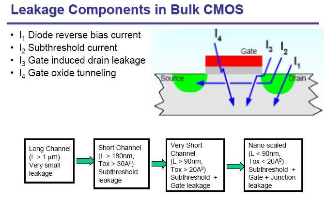
30 the reverse-bias diode leakage at the transistor drains and the sub-threshold current through an turnedoff transistor channel Log I D gate p+ p+ n-type substrate + V dd leakage current reversed-biased diode (drain-substrate) The leakage of a reverse-biased pmos transistor Subthreshold region Saturated region Decreasing V DS, V dd V GS, volts Subthreshold leakage with respect to gate-source voltage Design Course 29
31 30
32 the reverse-bias diode leakage at the transistor drains and the sub-threshold current through an turnedoff transistor channel Log I D gate p+ p+ n-type substrate + V dd leakage current reversed-biased diode (drain-substrate) The leakage of a reverse-biased pmos transistor Subthreshold region Saturated region Decreasing V DS, V dd V GS, volts Subthreshold leakage with respect to gate-source voltage Dimitrios Soudris, DUTH 31
![Power consumption of transfer and storage over datapath operations both in hardware [Men95] and software [Tiw94, Gon96]. 33 relative energy/operation 1 3.6 4.4 9 10 relative energy 0.4 0.2 0.](/docs-images/89/97649627/images/33-3.jpg "0 16-bit carry-select 16-bit Multiplier 8x128x16 SRAM (read) 8x128x16 SRAM (write) External I/O Access 16 bit Memory Access Storage Interconnect clocks Other RISC components Dimitrios Soudris,")
33 Power consumption of transfer and storage over datapath operations both in hardware [Men95] and software [Tiw94, Gon96]. 33 relative energy/operation relative energy bit carry-select 16-bit Multiplier 8x128x16 SRAM (read) 8x128x16 SRAM (write) External I/O Access 16 bit Memory Access Storage Interconnect clocks Other RISC components Dimitrios Soudris, 32
34 Increasing power savings System level x Behavior level RT level 2-5 x Logic level Transistor level 20-50% Layout level Design Course 33
35 Algorithm Transformation to exploit concurrency Architecture Parallelism and Pipelining Circuit/Logic Transistor Sizing, Fast Logic Structures Technology Threshold Voltage Reduction, Feature Size scaling Design Course 34
36 Syste m U Partitioning, Powe r-down, powe r state s Algorithm C omple xity, C oncurre ncy, Re gularity, Locality, Data re pre se ntation Archite cture C oncurre ncy, Instruction se t se le ction, Signal corre lations, Data re pre se ntation, Data Encoding C ircuit/logic Transistor siz ing, Logic optimiz ation, Powe r down, Layout O ptimiz ation Te chnology Advance d packaging, SO I Design Course 35
37 System Specifications System Specifications System-Level Design System-Level Design System-Level Analysis/Estimation Power models f or System -level com ponents Architecture-Level Design Logic-Level Design Architecture-Level Design Architecture-Level Analysis/Estimation Power models f or macrocells, control logic Logic-Level Design Circuit-Level Design / Layout synthesis Logic-Level Analysis/Estimation Power models f or gates, cells (a) Circuit-Level Design / Layout synthesis Circuit-Level Analysis/Estimation (b) Design Course 36
38 multiplier clock generator 2.0 m technology T d = C L * V dd I NORMALIZED DELAY adder ring oscillator adder (SPICE) microcoded DSP chip T d(vdd=2) = (2) * (5-0.7) 2 T d(vdd=5) I ~ (V dd - V t ) 2 4 (5) * (2-0.7) V dd (volts) Relatively independent of logic function and style. Design Course 37
 P x t d = E t = C L * V dd 2 E (Vdd=2) = E (Vdd=5) (C L ) * (2) 2 (C L ) * (5) 2 E (Vdd=2) 0.")
39 NORMALIZED POWER-DELAY PRODUCT quadratic dependence 51 stage ring oscillator 8-bit adder Vdd (volts) P x t d = E t = C L * V dd 2 E (Vdd=2) = E (Vdd=5) (C L ) * (2) 2 (C L ) * (5) 2 E (Vdd=2) 0.16 E (Vdd =5) Strong function of voltage (V 2 dependence). Relatively independent of logic function and style. Power Delay Product Improves with lowering V DD. Design Course 38
40 Delay I D 2V t V dd V t = 0 V t = 0.2 V GS Reduces the Speed Loss, But Increases Leakage Interesting Design Approach: DESIGN FOR P Leakage == P Dynamic Design Course 39
41 Lower Capacitance Small W/L s Higher Voltage Higher Capacitance Large W/L s Lower Voltage Larger sized devices are useful only when interconnect dominated. Minimum sized devices are usually optimal for low-power. Design Course 40
42 Global bus architecture Local bus architecture Shared Resources incur Switching Overhead Design Course 41
43 Power Consumption is Data Dependent Example: Static 2 Input NOR Gate Assume: P(A=1) = 1/2 P(B=1) = 1/2 Then: P(Out=1) = 1/4 P(0 1) = P(Out=0).P(Out=1) = 3/4 1/4 = 3/16 C EFF = 3/16 * C L Design Course 42

44 Design Course 43
45 A X B Z Reconvergence P(Z=1) = P(B=1). P(X=1 B=1) Becomes complex and intractable real fast Design Course 44
46 V DD M p Out In 1 In 2 In 3 PDN M e Power is Only Dissipated when Out=0! C EFF = P(Out=0).C L Design Course 45
47 Example: Dynamic 2 Input NOR Gate Assume: P(A=1) = 1/2 P(B=1) = 1/2 Then: P(Out=0) = 3/4 C EFF = 3/4 * C L Switching Activity Is Always Higher in Dynamic Circuits Design Course 46
48 Switching Activity for Precharged Dynamic Gates P 0 1 = P 0 Design Course 47

49
Low Power Design for Systems on a Chip. Tutorial Outline
 Low Power Design for Systems on a Chip Mary Jane Irwin Dept of CSE Penn State University (www.cse.psu.edu/~mji) Low Power Design for SoCs ASIC Tutorial Intro.1 Tutorial Outline Introduction and motivation
Low Power Design in VLSI
 Low Power Design in VLSI Evolution in Power Dissipation: Why worry about power? Heat Dissipation source : arpa-esto microprocessor power dissipation DEC 21164 Computers Defined by Watts not MIPS: µwatt
Low Power VLSI Circuit Synthesis: Introduction and Course Outline
 Low Power VLSI Circuit Synthesis: Introduction and Course Outline Ajit Pal Professor Department of Computer Science and Engineering Indian Institute of Technology Kharagpur INDIA -721302 Agenda Why Low
Low-Power Digital CMOS Design: A Survey
 Low-Power Digital CMOS Design: A Survey Krister Landernäs June 4, 2005 Department of Computer Science and Electronics, Mälardalen University Abstract The aim of this document is to provide the reader with
Low-Power CMOS VLSI Design
 Low-Power CMOS VLSI Design ( 范倫達 ), Ph. D. Department of Computer Science, National Chiao Tung University, Taiwan, R.O.C. Fall, 2017 ldvan@cs.nctu.edu.tw http://www.cs.nctu.tw/~ldvan/ Outline Introduction
Lecture 4. The CMOS Inverter. DC Transfer Curve: Load line. DC Operation: Voltage Transfer Characteristic. Noise in Digital Integrated Circuits
 Noise in Digital Integrated Circuits Lecture 4 The CMOS Inverter i(t) v(t) V DD Peter Cheung Department of Electrical & Electronic Engineering Imperial College London URL: www.ee.ic.ac.uk/pcheung/ E-mail:
Power Spring /7/05 L11 Power 1
 Power 6.884 Spring 2005 3/7/05 L11 Power 1 Lab 2 Results Pareto-Optimal Points 6.884 Spring 2005 3/7/05 L11 Power 2 Standard Projects Two basic design projects Processor variants (based on lab1&2 testrigs)
1. Short answer questions. (30) a. What impact does increasing the length of a transistor have on power and delay? Why? (6)
 a. What impact does increasing the length of a transistor have on power and delay? Why? (6)") CSE 493/593 Test 2 Fall 2011 Solution 1. Short answer questions. (30) a. What impact does increasing the length of a transistor have on power and delay? Why? (6) Decreasing of W to make the gate slower,
CSE 493/593 Test 2 Fall 2011 Solution 1. Short answer questions. (30) a. What impact does increasing the length of a transistor have on power and delay? Why? (6) Decreasing of W to make the gate slower,
LOW POWER VLSI TECHNIQUES FOR PORTABLE DEVICES Sandeep Singh 1, Neeraj Gupta 2, Rashmi Gupta 2
 LOW POWER VLSI TECHNIQUES FOR PORTABLE DEVICES Sandeep Singh 1, Neeraj Gupta 2, Rashmi Gupta 2 1 M.Tech Student, Amity School of Engineering & Technology, India 2 Assistant Professor, Amity School of Engineering
EE241 - Spring 2004 Advanced Digital Integrated Circuits. Announcements. Borivoje Nikolic. Lecture 15 Low-Power Design: Supply Voltage Scaling
 EE241 - Spring 2004 Advanced Digital Integrated Circuits Borivoje Nikolic Lecture 15 Low-Power Design: Supply Voltage Scaling Announcements Homework #2 due today Midterm project reports due next Thursday
Leakage Power Reduction for Logic Circuits Using Variable Body Biasing Technique
 Leakage Power Reduction for Logic Circuits Using Variable Body Biasing Technique Anjana R 1 and Ajay K Somkuwar 2 Assistant Professor, Department of Electronics and Communication, Dr. K.N. Modi University,
Innovations In Techniques And Design Strategies For Leakage And Overall Power Reduction In Cmos Vlsi Circuits: A Review
 Innovations In Techniques And Design Strategies For Leakage And Overall Power Reduction In Cmos Vlsi Circuits: A Review SUPRATIM SAHA Assistant Professor, Department of ECE, Subharti Institute of Technology
Design of Low Power Vlsi Circuits Using Cascode Logic Style
 Design of Low Power Vlsi Circuits Using Cascode Logic Style Revathi Loganathan 1, Deepika.P 2, Department of EST, 1 -Velalar College of Enginering & Technology, 2- Nandha Engineering College,Erode,Tamilnadu,India
Low Power Realization of Subthreshold Digital Logic Circuits using Body Bias Technique
 Indian Journal of Science and Technology, Vol 9(5), DOI: 1017485/ijst/2016/v9i5/87178, Februaru 2016 ISSN (Print) : 0974-6846 ISSN (Online) : 0974-5645 Low Power Realization of Subthreshold Digital Logic
Power dissipation in CMOS
 DC Current in For V IN < V TN, N O is cut off and I DD = 0. For V TN < V IN < V DD /2, N O is saturated. For V DD /2 < V IN < V DD +V TP, P O is saturated. For V IN > V DD + V TP, P O is cut off and I
EE 330 Lecture 43. Digital Circuits. Other Logic Styles Dynamic Logic Circuits
 EE 330 Lecture 43 Digital Circuits Other Logic Styles Dynamic Logic Circuits Review from Last Time Elmore Delay Calculations W M 5 V OUT x 20C RE V IN 0 L R L 1 L R R 6 W 1 C C 3 D R t 1 R R t 2 R R t
Homework 10 posted just for practice. Office hours next week, schedule TBD. HKN review today. Your feedback is important!
 EE141 Fall 2005 Lecture 26 Memory (Cont.) Perspectives Administrative Stuff Homework 10 posted just for practice No need to turn in Office hours next week, schedule TBD. HKN review today. Your feedback
Low Power Design Part I Introduction and VHDL design. Ricardo Santos LSCAD/FACOM/UFMS
 Low Power Design Part I Introduction and VHDL design Ricardo Santos ricardo@facom.ufms.br LSCAD/FACOM/UFMS Motivation for Low Power Design Low power design is important from three different reasons Device
Novel Buffer Design for Low Power and Less Delay in 45nm and 90nm Technology
 Novel Buffer Design for Low Power and Less Delay in 45nm and 90nm Technology 1 Mahesha NB #1 #1 Lecturer Department of Electronics & Communication Engineering, Rai Technology University nbmahesh512@gmail.com
Chapter 1 Introduction
 Chapter 1 Introduction 1.1 Introduction There are many possible facts because of which the power efficiency is becoming important consideration. The most portable systems used in recent era, which are
Design of 32-bit ALU using Low Power Energy Efficient Full Adder Circuits
 Design of 32-bit ALU using Low Power Energy Efficient Full Adder Circuits Priyadarshini.V Department of ECE Gudlavalleru Engieering College,Gudlavalleru darshiniv708@gmail.com Ramya.P Department of ECE
Sleepy Keeper Approach for Power Performance Tuning in VLSI Design
 International Journal of Electronics and Communication Engineering. ISSN 0974-2166 Volume 6, Number 1 (2013), pp. 17-28 International Research Publication House http://www.irphouse.com Sleepy Keeper Approach
Temperature-adaptive voltage tuning for enhanced energy efficiency in ultra-low-voltage circuits
 Microelectronics Journal 39 (2008) 1714 1727 www.elsevier.com/locate/mejo Temperature-adaptive voltage tuning for enhanced energy efficiency in ultra-low-voltage circuits Ranjith Kumar, Volkan Kursun Department
EE 330 Lecture 43. Digital Circuits. Other Logic Styles Dynamic Logic Circuits
 EE 330 Lecture 43 Digital Circuits Other Logic Styles Dynamic Logic Circuits Review from Last Time Elmore Delay Calculations W M 5 V OUT x 20C RE V IN 0 L R L 1 L R RW 6 W 1 C C 3 D R t 1 R R t 2 R R t
EEC 118 Lecture #12: Dynamic Logic
 EEC 118 Lecture #12: Dynamic Logic Rajeevan Amirtharajah University of California, Davis Jeff Parkhurst Intel Corporation Outline Today: Alternative MOS Logic Styles Dynamic MOS Logic Circuits: Rabaey
A Static Power Model for Architects
 A Static Power Model for Architects J. Adam Butts and Guri Sohi University of Wisconsin-Madison {butts,sohi}@cs.wisc.edu 33rd International Symposium on Microarchitecture Monterey, California December,
Dynamic Logic. Domino logic P-E logic NORA logic 2-phase logic Multiple O/P domino logic Cascode logic 11/28/2012 1
 Dynamic Logic Dynamic Circuits will be introduced and their performance in terms of power, area, delay, energy and AT 2 will be reviewed. We will review the following logic families: Domino logic P-E logic
A Survey of the Low Power Design Techniques at the Circuit Level
 A Survey of the Low Power Design Techniques at the Circuit Level Hari Krishna B Assistant Professor, Department of Electronics and Communication Engineering, Vagdevi Engineering College, Warangal, India
UNIT-II LOW POWER VLSI DESIGN APPROACHES
 UNIT-II LOW POWER VLSI DESIGN APPROACHES Low power Design through Voltage Scaling: The switching power dissipation in CMOS digital integrated circuits is a strong function of the power supply voltage.
DIGITAL INTEGRATED CIRCUITS A DESIGN PERSPECTIVE 2 N D E D I T I O N
 DIGITAL INTEGRATED CIRCUITS A DESIGN PERSPECTIVE 2 N D E D I T I O N Jan M. Rabaey, Anantha Chandrakasan, and Borivoje Nikolic CONTENTS PART I: THE FABRICS Chapter 1: Introduction (32 pages) 1.1 A Historical
Energy-Recovery CMOS Design
 Energy-Recovery CMOS Design Jay Moon, Bill Athas * Univ of Southern California * Apple Computer, Inc. jsmoon@usc.edu / athas@apple.com March 05, 2001 UCLA EE215B jsmoon@usc.edu / athas@apple.com 1 Outline
Power and Energy. Courtesy of Dr. Daehyun Dr. Dr. Shmuel and Dr.
 Power and Energy Courtesy of Dr. Daehyun Lim@WSU, Dr. Harris@HMC, Dr. Shmuel Wimer@BIU and Dr. Choi@PSU http://csce.uark.edu +1 (479) 575-6043 yrpeng@uark.edu The Chip is HOT Power consumption increases
International Journal of Advanced Research in Computer Science and Software Engineering
 Volume 3, Issue 8, August 2013 ISSN: 2277 128X International Journal of Advanced Research in Computer Science and Software Engineering Research Paper Available online at: www.ijarcsse.com A Novel Implementation
EECS 427 Lecture 13: Leakage Power Reduction Readings: 6.4.2, CBF Ch.3. EECS 427 F09 Lecture Reminders
 EECS 427 Lecture 13: Leakage Power Reduction Readings: 6.4.2, CBF Ch.3 [Partly adapted from Irwin and Narayanan, and Nikolic] 1 Reminders CAD assignments Please submit CAD5 by tomorrow noon CAD6 is due
Design of low power SRAM Cell with combined effect of sleep stack and variable body bias technique
 Design of low power SRAM Cell with combined effect of sleep stack and variable body bias technique Anjana R 1, Dr. Ajay kumar somkuwar 2 1 Asst.Prof & ECE, Laxmi Institute of Technology, Gujarat 2 Professor
Designing of Low-Power VLSI Circuits using Non-Clocked Logic Style
 International Journal of Advancements in Research & Technology, Volume 1, Issue3, August-2012 1 Designing of Low-Power VLSI Circuits using Non-Clocked Logic Style Vishal Sharma #, Jitendra Kaushal Srivastava
Total reduction of leakage power through combined effect of Sleep stack and variable body biasing technique
 Total reduction of leakage power through combined effect of Sleep and variable body biasing technique Anjana R 1, Ajay kumar somkuwar 2 Abstract Leakage power consumption has become a major concern for
NOVEL OSCILLATORS IN SUBTHRESHOLD REGIME
 NOVEL OSCILLATORS IN SUBTHRESHOLD REGIME Neeta Pandey 1, Kirti Gupta 2, Rajeshwari Pandey 3, Rishi Pandey 4, Tanvi Mittal 5 1, 2,3,4,5 Department of Electronics and Communication Engineering, Delhi Technological
UNIT-1 Fundamentals of Low Power VLSI Design
 UNIT-1 Fundamentals of Low Power VLSI Design Need for Low Power Circuit Design: The increasing prominence of portable systems and the need to limit power consumption (and hence, heat dissipation) in very-high
CHAPTER 3 PERFORMANCE OF A TWO INPUT NAND GATE USING SUBTHRESHOLD LEAKAGE CONTROL TECHNIQUES
 CHAPTER 3 PERFORMANCE OF A TWO INPUT NAND GATE USING SUBTHRESHOLD LEAKAGE CONTROL TECHNIQUES 41 In this chapter, performance characteristics of a two input NAND gate using existing subthreshold leakage
19. Design for Low Power
 19. Design for Low Power Jacob Abraham Department of Electrical and Computer Engineering The University of Texas at Austin VLSI Design Fall 2017 November 8, 2017 ECE Department, University of Texas at
Robust Subthreshold Circuit Designing Using Sub-threshold Source Coupled Logic (STSCL)
") International Journal of Electronics Engineering, (1), 010, pp. 19-3 Robust Subthreshold Circuit Designing Using Sub-threshold Source Coupled Logic (STSCL) Ashutosh Nandi 1, Gaurav Saini, Amit Kumar Jaiswal
International Journal of Electronics Engineering, (1), 010, pp. 19-3 Robust Subthreshold Circuit Designing Using Sub-threshold Source Coupled Logic (STSCL) Ashutosh Nandi 1, Gaurav Saini, Amit Kumar Jaiswal
EEC 216 Lecture #10: Ultra Low Voltage and Subthreshold Circuit Design. Rajeevan Amirtharajah University of California, Davis
 EEC 216 Lecture #1: Ultra Low Voltage and Subthreshold Circuit Design Rajeevan Amirtharajah University of California, Davis Opportunities for Ultra Low Voltage Battery Operated and Mobile Systems Wireless
Contents 1 Introduction 2 MOS Fabrication Technology
 Contents 1 Introduction... 1 1.1 Introduction... 1 1.2 Historical Background [1]... 2 1.3 Why Low Power? [2]... 7 1.4 Sources of Power Dissipations [3]... 9 1.4.1 Dynamic Power... 10 1.4.2 Static Power...
Announcements. Advanced Digital Integrated Circuits. Midterm feedback mailed back Homework #3 posted over the break due April 8
 EE241 - Spring 21 Advanced Digital Integrated Circuits Lecture 18: Dynamic Voltage Scaling Announcements Midterm feedback mailed back Homework #3 posted over the break due April 8 Reading: Chapter 5, 6,
EECS 427 Lecture 22: Low and Multiple-Vdd Design
 EECS 427 Lecture 22: Low and Multiple-Vdd Design Reading: 11.7.1 EECS 427 W07 Lecture 22 1 Last Time Low power ALUs Glitch power Clock gating Bus recoding The low power design space Dynamic vs static EECS
Low Power High Performance 10T Full Adder for Low Voltage CMOS Technology Using Dual Threshold Voltage
 Low Power High Performance 10T Full Adder for Low Voltage CMOS Technology Using Dual Threshold Voltage Surbhi Kushwah 1, Shipra Mishra 2 1 M.Tech. VLSI Design, NITM College Gwalior M.P. India 474001 2
Combinational Logic Gates in CMOS
 Combinational Logic Gates in CMOS References: dapted from: Digital Integrated Circuits: Design Perspective, J. Rabaey UC Principles of CMOS VLSI Design: Systems Perspective, 2nd Ed., N. H. E. Weste and
Lecture 13 CMOS Power Dissipation
 EE 471: Transport Phenomena in Solid State Devices Spring 2018 Lecture 13 CMOS Power Dissipation Bryan Ackland Department of Electrical and Computer Engineering Stevens Institute of Technology Hoboken,
Announcements. Advanced Digital Integrated Circuits. Quiz #3 today Homework #4 posted This lecture until 4pm
 EE241 - Spring 2011 dvanced Digital Integrated Circuits Lecture 20: High-Performance Logic Styles nnouncements Quiz #3 today Homework #4 posted This lecture until 4pm Reading: Chapter 8 in the owhill text
Topic 6. CMOS Static & Dynamic Logic Gates. Static CMOS Circuit. NMOS Transistors in Series/Parallel Connection
 NMOS Transistors in Series/Parallel Connection Topic 6 CMOS Static & Dynamic Logic Gates Peter Cheung Department of Electrical & Electronic Engineering Imperial College London Transistors can be thought
Reduce Power Consumption for Digital Cmos Circuits Using Dvts Algoritham
 IOSR Journal of Electrical and Electronics Engineering (IOSR-JEEE) e-issn: 2278-1676,p-ISSN: 2320-3331, Volume 10, Issue 5 Ver. II (Sep Oct. 2015), PP 109-115 www.iosrjournals.org Reduce Power Consumption
Improved Two Phase Clocked Adiabatic Static CMOS Logic Circuit
 Available online www.ejaet.com European Journal of Advances in Engineering and Technology, 2017, 4 (5): 319-325 Research Article ISSN: 2394-658X Improved Two Phase Clocked Adiabatic Static CMOS Logic Circuit
Design & Analysis of Low Power Full Adder
 1174 Design & Analysis of Low Power Full Adder Sana Fazal 1, Mohd Ahmer 2 1 Electronics & communication Engineering Integral University, Lucknow 2 Electronics & communication Engineering Integral University,
An Analysis of Novel CMOS Ring Oscillator Using LECTOR Technique with Minimum Leakage
 Available online www.ejaet.com European Journal of Advances in Engineering and Technology, 2017, 4 (1): 44-48 Research Article ISSN: 2394-658X An Analysis of Novel CMOS Ring Oscillator Using LECTOR Technique
Propagation Delay, Circuit Timing & Adder Design. ECE 152A Winter 2012
 Propagation Delay, Circuit Timing & Adder Design ECE 152A Winter 2012 Reading Assignment Brown and Vranesic 2 Introduction to Logic Circuits 2.9 Introduction to CAD Tools 2.9.1 Design Entry 2.9.2 Synthesis
Chapter 6 Combinational CMOS Circuit and Logic Design. Jin-Fu Li Department of Electrical Engineering National Central University Jungli, Taiwan
 Chapter 6 Combinational CMOS Circuit and Logic Design Jin-Fu Li Department of Electrical Engineering National Central University Jungli, Taiwan Outline Advanced Reliable Systems (ARES) Lab. Jin-Fu Li,
Propagation Delay, Circuit Timing & Adder Design
 Propagation Delay, Circuit Timing & Adder Design ECE 152A Winter 2012 Reading Assignment Brown and Vranesic 2 Introduction to Logic Circuits 2.9 Introduction to CAD Tools 2.9.1 Design Entry 2.9.2 Synthesis
EEC 118 Lecture #11: CMOS Design Guidelines Alternative Static Logic Families
 EEC 118 Lecture #11: CMOS Design Guidelines Alternative Static Logic Families Rajeevan Amirtharajah University of California, Davis Jeff Parkhurst Intel Corporation Announcements Homework 5 this week Lab
Design and Implementation of Pipelined 4-Bit Binary Multiplier Using M.G.D.I. Technique
 Volume 2 Issue 3 September 2014 ISSN: 2320-9984 (Online) International Journal of Modern Engineering & Management Research Website: www.ijmemr.org Design and Implementation of Pipelined 4-Bit Binary Multiplier
Opportunities and Challenges in Ultra Low Voltage CMOS. Rajeevan Amirtharajah University of California, Davis
 Opportunities and Challenges in Ultra Low Voltage CMOS Rajeevan Amirtharajah University of California, Davis Opportunities for Ultra Low Voltage Battery Operated and Mobile Systems Wireless sensors RFID
A gate sizing and transistor fingering strategy for
 LETTER IEICE Electronics Express, Vol.9, No.19, 1550 1555 A gate sizing and transistor fingering strategy for subthreshold CMOS circuits Morteza Nabavi a) and Maitham Shams b) Department of Electronics,
Low Power Techniques for SoC Design: basic concepts and techniques
 Low Power Techniques for SoC Design: basic concepts and techniques Estagiário de Docência M.Sc. Vinícius dos Santos Livramento Prof. Dr. Luiz Cláudio Villar dos Santos Embedded Systems - INE 5439 Federal
DESIGN FOR LOW-POWER USING MULTI-PHASE AND MULTI- FREQUENCY CLOCKING
 3 rd Int. Conf. CiiT, Molika, Dec.12-15, 2002 31 DESIGN FOR LOW-POWER USING MULTI-PHASE AND MULTI- FREQUENCY CLOCKING M. Stojčev, G. Jovanović Faculty of Electronic Engineering, University of Niš Beogradska
Minimizing the Sub Threshold Leakage for High Performance CMOS Circuits Using Stacked Sleep Technique
 International Journal of Electrical Engineering. ISSN 0974-2158 Volume 10, Number 3 (2017), pp. 323-335 International Research Publication House http://www.irphouse.com Minimizing the Sub Threshold Leakage
Low Power, Area Efficient FinFET Circuit Design
 Low Power, Area Efficient FinFET Circuit Design Michael C. Wang, Princeton University Abstract FinFET, which is a double-gate field effect transistor (DGFET), is more versatile than traditional single-gate
COMPARISON AMONG DIFFERENT CMOS INVERTER WITH STACK KEEPER APPROACH IN VLSI DESIGN
 Journal of Engineering Research and Applications (IJERA) ISSN: 2248-9622 www.ijera.com COMPARISON AMONG DIFFERENT INVERTER WITH STACK KEEPER APPROACH IN VLSI DESIGN HARSHVARDHAN UPADHYAY* ABHISHEK CHOUBEY**
Introduction. Digital Integrated Circuits A Design Perspective. Jan M. Rabaey Anantha Chandrakasan Borivoje Nikolic. July 30, 2002
 Digital Integrated Circuits A Design Perspective Jan M. Rabaey Anantha Chandrakasan Borivoje Nikolic Introduction July 30, 2002 1 What is this book all about? Introduction to digital integrated circuits.
Course Content. Course Content. Course Format. Low Power VLSI System Design Lecture 1: Introduction. Course focus
 Course Content Low Power VLSI System Design Lecture 1: Introduction Prof. R. Iris Bahar E September 6, 2017 Course focus low power and thermal-aware design digital design, from devices to architecture
DESIGNING OF SRAM USING LECTOR TECHNIQUE TO REDUCE LEAKAGE POWER
 DESIGNING OF SRAM USING LECTOR TECHNIQUE TO REDUCE LEAKAGE POWER Ashwini Khadke 1, Paurnima Chaudhari 2, Mayur More 3, Prof. D.S. Patil 4 1Pursuing M.Tech, Dept. of Electronics and Engineering, NMU, Maharashtra,
A NEW APPROACH FOR DELAY AND LEAKAGE POWER REDUCTION IN CMOS VLSI CIRCUITS
 http:// A NEW APPROACH FOR DELAY AND LEAKAGE POWER REDUCTION IN CMOS VLSI CIRCUITS Ruchiyata Singh 1, A.S.M. Tripathi 2 1,2 Department of Electronics and Communication Engineering, Mangalayatan University
Topics. Low Power Techniques. Based on Penn State CSE477 Lecture Notes 2002 M.J. Irwin and adapted from Digital Integrated Circuits 2002 J.
 Topics Low Power Techniques Based on Penn State CSE477 Lecture Notes 2002 M.J. Irwin and adapted from Digital Integrated Circuits 2002 J. Rabaey Review: Energy & Power Equations E = C L V 2 DD P 0 1 +
IMPLEMENTATION OF ADIABATIC DYNAMIC LOGIC IN BIT FULL ADDER
 Technology and Innovation for Sustainable Development Conference (TISD2006) Faculty of Engineering, Khon Kaen University, Thailand 25-26 January 2006 IMPLEMENTATION OF ADIABATIC DYNAMIC LOGIC IN BIT FULL
Lecture 12 Memory Circuits. Memory Architecture: Decoders. Semiconductor Memory Classification. Array-Structured Memory Architecture RWM NVRWM ROM
 Semiconductor Memory Classification Lecture 12 Memory Circuits RWM NVRWM ROM Peter Cheung Department of Electrical & Electronic Engineering Imperial College London Reading: Weste Ch 8.3.1-8.3.2, Rabaey
Comparison of Power Dissipation in inverter using SVL Techniques
 Comparison of Power Dissipation in inverter using SVL Techniques K. Kalai Selvi Assistant Professor, Dept. of Electronics & Communication Engineering, Government College of Engineering, Tirunelveli, India
Robust Ultra-Low Power Sub-threshold DTMOS Logic Λ
 Robust Ultra-Low Power Sub-threshold DTMOS Logic Λ Hendrawan Soeleman, Kaushik Roy, and Bipul Paul Purdue University Department of Electrical and Computer Engineering West Lafayette, IN 797, USA fsoeleman,
LOW POWER CMOS CELL STRUCTURES BASED ON ADIABATIC SWITCHING
 LOW POWER CMOS CELL STRUCTURES BASED ON ADIABATIC SWITCHING Uday Kumar Rajak Electronics & Telecommunication Dept. Columbia Institute of Engineering and Technology,Raipur (India) ABSTRACT The dynamic power
EE 330 Lecture 44. Digital Circuits. Other Logic Styles Dynamic Logic Circuits
 EE 330 Lecture 44 Digital Circuits Other Logic Styles Dynamic Logic Circuits Course Evaluation Reminder - ll Electronic http://bit.ly/isustudentevals Review from Last Time Power Dissipation in Logic Circuits
ECE 334: Electronic Circuits Lecture 10: Digital CMOS Circuits
 Faculty of Engineering ECE 334: Electronic Circuits Lecture 10: Digital CMOS Circuits CMOS Technology Complementary MOS, or CMOS, needs both PMOS and NMOS FET devices for their logic gates to be realized
CMPEN 411 VLSI Digital Circuits Spring Lecture 24: Peripheral Memory Circuits
 CMPEN 411 VLSI Digital Circuits Spring 2011 Lecture 24: Peripheral Memory Circuits [Adapted from Rabaey s Digital Integrated Circuits, Second Edition, 2003 J. Rabaey, A. Chandrakasan, B. Nikolic] Sp11
EE 42/100 Lecture 23: CMOS Transistors and Logic Gates. Rev A 4/15/2012 (10:39 AM) Prof. Ali M. Niknejad
 Prof. Ali M. Niknejad") A. M. Niknejad University of California, Berkeley EE 100 / 42 Lecture 23 p. 1/16 EE 42/100 Lecture 23: CMOS Transistors and Logic Gates ELECTRONICS Rev A 4/15/2012 (10:39 AM) Prof. Ali M. Niknejad University
A. M. Niknejad University of California, Berkeley EE 100 / 42 Lecture 23 p. 1/16 EE 42/100 Lecture 23: CMOS Transistors and Logic Gates ELECTRONICS Rev A 4/15/2012 (10:39 AM) Prof. Ali M. Niknejad University
Datorstödd Elektronikkonstruktion
 Datorstödd Elektronikkonstruktion [Computer Aided Design of Electronics] Zebo Peng, Petru Eles and Gert Jervan Embedded Systems Laboratory IDA, Linköping University http://www.ida.liu.se/~tdts80/~tdts80
Data Word Length Reduction for Low-Power DSP Software
 EE382C: LITERATURE SURVEY, APRIL 2, 2004 1 Data Word Length Reduction for Low-Power DSP Software Kyungtae Han Abstract The increasing demand for portable computing accelerates the study of minimizing power
International Journal of Advanced Research in Biology Engineering Science and Technology (IJARBEST)
") Abstract NEW HIGH PERFORMANCE 4 BIT PARALLEL ADDER USING DOMINO LOGIC Department Of Electronics and Communication Engineering UG Scholar, SNS College of Engineering Bhuvaneswari.N [1], Hemalatha.V [2],
Abstract NEW HIGH PERFORMANCE 4 BIT PARALLEL ADDER USING DOMINO LOGIC Department Of Electronics and Communication Engineering UG Scholar, SNS College of Engineering Bhuvaneswari.N [1], Hemalatha.V [2],
A Digital Clock Multiplier for Globally Asynchronous Locally Synchronous Designs
 A Digital Clock Multiplier for Globally Asynchronous Locally Synchronous Designs Thomas Olsson, Peter Nilsson, and Mats Torkelson. Dept of Applied Electronics, Lund University. P.O. Box 118, SE-22100,
An Overview of Static Power Dissipation
 An Overview of Static Power Dissipation Jayanth Srinivasan 1 Introduction Power consumption is an increasingly important issue in general purpose processors, particularly in the mobile computing segment.
Static Energy Reduction Techniques in Microprocessor Caches
 Static Energy Reduction Techniques in Microprocessor Caches Heather Hanson, Stephen W. Keckler, Doug Burger Computer Architecture and Technology Laboratory Department of Computer Sciences Tech Report TR2001-18
1 Digital EE141 Integrated Circuits 2nd Introduction
 Digital Integrated Circuits Introduction 1 What is this lecture about? Introduction to digital integrated circuits + low power circuits Issues in digital design The CMOS inverter Combinational logic structures
STUDY OF VOLTAGE AND CURRENT SENSE AMPLIFIER
 STUDY OF VOLTAGE AND CURRENT SENSE AMPLIFIER Sandeep kumar 1, Charanjeet Singh 2 1,2 ECE Department, DCRUST Murthal, Haryana Abstract Performance of sense amplifier has considerable impact on the speed
ELEC Digital Logic Circuits Fall 2015 Delay and Power
 ELEC - Digital Logic Circuits Fall 5 Delay and Power Vishwani D. Agrawal James J. Danaher Professor Department of Electrical and Computer Engineering Auburn University, Auburn, AL 36849 http://www.eng.auburn.edu/~vagrawal
Performance Analysis of Different Adiabatic Logic Families
 Performance Analysis of Different Adiabatic Logic Families 1 Anitha.K, 2 Dr.Meena Srinivasan 1 PG Scholar, 2 Associate Professor Electronics and Communication Engineering Government College of Technology,
EMT 251 Introduction to IC Design
 EMT 251 Introduction to IC Design (Pengantar Rekabentuk Litar Terkamir) Semester II 2011/2012 Introduction to IC design and Transistor Fundamental Some Keywords! Very-large-scale-integration (VLSI) is
CPE/EE 427, CPE 527 VLSI Design I: Homeworks 3 & 4
 CPE/EE 427, CPE 527 VLSI Design I: Homeworks 3 & 4 1 2 3 4 5 6 7 8 9 10 Sum 30 10 25 10 30 40 10 15 15 15 200 1. (30 points) Misc, Short questions (a) (2 points) Postponing the introduction of signals
Leakage Current Analysis
 Current Analysis Hao Chen, Latriese Jackson, and Benjamin Choo ECE632 Fall 27 University of Virginia , , @virginia.edu Abstract Several common leakage current reduction methods such
DYNAMIC VOLTAGE FREQUENCY SCALING (DVFS) FOR MICROPROCESSORS POWER AND ENERGY REDUCTION
 FOR MICROPROCESSORS POWER AND ENERGY REDUCTION") DYNAMIC VOLTAGE FREQUENCY SCALING (DVFS) FOR MICROPROCESSORS POWER AND ENERGY REDUCTION Diary R. Suleiman Muhammed A. Ibrahim Ibrahim I. Hamarash e-mail: diariy@engineer.com e-mail: ibrahimm@itu.edu.tr
DYNAMIC VOLTAGE FREQUENCY SCALING (DVFS) FOR MICROPROCESSORS POWER AND ENERGY REDUCTION Diary R. Suleiman Muhammed A. Ibrahim Ibrahim I. Hamarash e-mail: diariy@engineer.com e-mail: ibrahimm@itu.edu.tr
CHAPTER 5 DESIGN AND ANALYSIS OF COMPLEMENTARY PASS- TRANSISTOR WITH ASYNCHRONOUS ADIABATIC LOGIC CIRCUITS
 70 CHAPTER 5 DESIGN AND ANALYSIS OF COMPLEMENTARY PASS- TRANSISTOR WITH ASYNCHRONOUS ADIABATIC LOGIC CIRCUITS A novel approach of full adder and multipliers circuits using Complementary Pass Transistor
Novel Low-Overhead Operand Isolation Techniques for Low-Power Datapath Synthesis
 Novel Low-Overhead Operand Isolation Techniques for Low-Power Datapath Synthesis N. Banerjee, A. Raychowdhury, S. Bhunia, H. Mahmoodi, and K. Roy School of Electrical and Computer Engineering, Purdue University,
Dual-K K Versus Dual-T T Technique for Gate Leakage Reduction : A Comparative Perspective
 Dual-K K Versus Dual-T T Technique for Gate Leakage Reduction : A Comparative Perspective S. P. Mohanty, R. Velagapudi and E. Kougianos Dept of Computer Science and Engineering University of North Texas
ECE 471/571 The CMOS Inverter Lecture-6. Gurjeet Singh
 ECE 471/571 The CMOS Inverter Lecture-6 Gurjeet Singh NMOS-to-PMOS ratio,pmos are made β times larger than NMOS Sizing Inverters for Performance Conclusions: Intrinsic delay tp0 is independent of sizing
Lecture 16. Complementary metal oxide semiconductor (CMOS) CMOS 1-1
 CMOS 1-1") Lecture 16 Complementary metal oxide semiconductor (CMOS) CMOS 1-1 Outline Complementary metal oxide semiconductor (CMOS) Inverting circuit Properties Operating points Propagation delay Power dissipation
Lecture 16 Complementary metal oxide semiconductor (CMOS) CMOS 1-1 Outline Complementary metal oxide semiconductor (CMOS) Inverting circuit Properties Operating points Propagation delay Power dissipation