Lecture 07 Modeling and Optimization of VLSI Interconnects (ECG 415/615 Introduction to VLSI System Design)
|
|
|
- Margery Shepherd
- 6 years ago
- Views:
Transcription
1 Lecture 07 Modeling and Optimization of VLSI Interconnects (ECG 415/615 Introduction to VLSI System Design) Dr. Yingtao Jiang Department of Electrical and Computer Engineering University of Nevada Las Vegas Spring, 2006
2 Objectives Understand the importance of interconnects in VLSI systems Learn how interconnects scale Learn how interconnect delay and power are modeled Resistance Capacitance Inductance Learn how interconnect delay and power are optimized at various levels

3 Interconnect Impact on Chip
4 Wire Models All-inclusive model Capacitance-only
5 Impact of Interconnect Parasitics Interconnect parasitics reduce reliability affect performance and power consumption Classes of parasitics Capacitive Resistive Inductive
6 Nature of Interconnect Local Interconnect Pentium Pro (R) Pentium(R) II Pentium (MMX) Pentium (R) Pentium (R) II No of nets (Log Scale) S Local = S Technology Global Interconnect S Global = S Die Source: Intel ,000 10, ,000 Length (u)
7 Readings H. B. Bakoglu, Circuits interconnects and packaging for VLSI, Addison Wesley W. J. Dally and J. W. Poulton, Digital Systems Engineering, Cambridge Press J. M. Rabaey, Digital Integrated circuits : A design perspective, Prentice Hall A. Chandrakasan, W. J. Bowhill, F. Fox, Design of High-Performance Microprocessor Circuits, IEEE Press

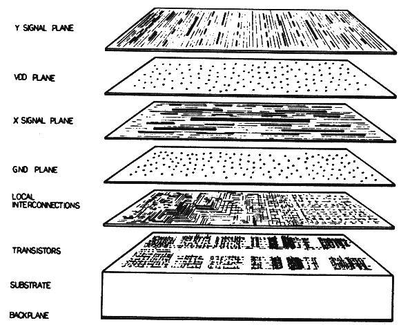
8 Components of VLSI system Logic Functional Block Router Logic Logic Gates Transistors Interconnects L2 Cache Cache Tags L2 Cache Power/ground and Clock Inter-block Signals Intra-block Signals Processor Core

9 Delay with technology scaling This figure is from the ITRS Roadmap on interconnects
10 Wire Delay
11 Wire Delay in the 35-nm Technology For the 35-nm technology generation using a copper conductor, a low- κ dielectric with κ=2, and a benchmark length L = 1.0 mm the interconnects RC response time is τ 250 ps. In comparison, the switching delay or latency of a minimum-geometry 35-nm generation MOSFET is τ d 2.5 ps.
12 Interconnect dimension trends in terms of IC generations These figures are derived from Design of High-Performance Microprocessor Circuits, A. Chandrakasan, W. Bowhill, F. Fox, IEEE, 2001
13 Trends in some integrated circuit parameters Local wiring pitch (nm) Chip size at production (mm 2 ) Total interconnect length (m/cm 2 ) On-chip local clock (GHz) Number of metal levels Maximum power (W) Package pin-count (high-performance)
14 Rent s rule Rent s rule relates the I/O requirement to the number of gates as : N = K p p As technology scales number of gates in a given area is increasing. More routing is required as technology scales. N β g
15 Nature of the interconnect Local Interconnect Number of wires Donath Occupation prob. Measurement Global Interconnect Wire length These figures are derived from Digital integrated circuit a design perspective, J. Rabaey Prentice Hall and a tutorial in SLIP by Dirk Stroobandt respectively
16 Interconnect Topologies A[0] Multi-sink A[1] A[63]... Bus or Routing Channel Grid Multi-source


17 Modern interconnect These figures are derived from Digital integrated circuit a design perspective, J. Rabaey Prentice Hall and ITRS roadmap on interconnect respectively

18 Multiple Interconnect Layers
19 Interconnects are critical Chip Area Increasing. Average physical length increasing. Electrical length of interconnects increasing faster than physical length. Number of Interconnects increasing. Longer and more wires imply more delay (RC) and power ( C L V 2 DD f )
20 Interconnect Solutions Design Methods - Timing Driven Floorplanning Devices - Improved I dsat, Dual V t Materials - Copper Interconnect, Low K Dielectric Geometries - Tall wires, Layers of metals, Shields Signaling Methods - Differential, Limited Swing Novel Methods - Wireless communication, Optical Interconnects
21 VLSI Design Cycle Chip Specs Partitioning Floorplan RTL Synthesis Timing Analysis Timing met Layout Extraction Timing Analysis Timing met Chip Tape out
22 Interconnect Focused Floorplanning Architectural Performance Sensitivity to Interconnect Delay Early Floorplanning Impact of New Circuit Techniques Interconnect-aware Architecture Design
23 Wire Models Why do we need models? Models simplify analysis and simulation. Why model wires? Estimate the delay due to wire. Check for signal integrity and reliability. What are the implications of a wrong model? Delay estimates can be wrong leading to slow or fast failures. Might lead to over or under driving leading to power dissipation and reliability concerns.
24 Ideal Model Wires are lines on schematics having no electrical effect. A voltage change at one end appears at its other end without any delay i.e. wire is a equipotential region. Ideal model simplistic Most wires connect local gates hence are short Ideal model might be ok For long i.e. global interconnects ideal model is absolutely wrong.
25 Early Models Wire width feature size Older technology had wide wires More cross-section area implies less resistance and more capacitance. Model wire only with capacitance H W L
26 However With scaling, width of wire reduced. Resistance of the wire no longer negligible. Wire not very long and a lumped RC is good enough approximation. L H W
27 Interconnect Resistance H L R = ρl HW W Ohm s Law: Resistance of wire wire length (L) and 1/ cross-section(hw) ρ (resistivity) is the property of the material.
28 Sheet Resistance Wire height (H) is constant for a technology. Sheet resistance (R q ) is constant for each metal layer. Calculation of wire resistance is easy : multiply R q by L/W R with R q = = R q ρ H L W
29 Interconnect Resistance
30 Dealing with Resistance Selective Technology Scaling Use Better Interconnect Materials reduce average wire-length e.g. copper, silicides More Interconnect Layers reduce average wire-length
31 Polycide Gate Mosfet Silicide PolySilicon SiO 2 n + n + p Silicides: WSi 2, TiSi 2, PtSi 2 and TaSi Conductivity: 8-10 times better than Poly
32 Sheet Resistance

33 Example: Intel 0.25 micron Process 5 metal layers Ti/Al - Cu/Ti/TiN Polysilicon dielectric
34 Interconnect Capacitance Capacitance of a wire = f (Shape, Distance to surrounding wires, Distance to the substrate ) Estimating Capacitance is a non-trivial task subject of active research. To get an accurate estimate electric field solvers (2D or 3D) should be used. Solving fields is slow and will take ages for estimating capacitance of the whole chip. Various assumptions and approximations used to get quick estimates.
35 Area Capacitance Current W L H t di Dielectric Electric Fields Substrate C int = ε di t di WL
36 Permittivity
37 Fringing Capacitance Fringing Fields H w Conductor + C wire = C pp + C fringe = 2πε log( t / di di H ) + wε t di di w W-H/2
38 Detailed Picture Is this much of detail required How to compute this?
39 Impact of Interwire Capacitance (from [Bakoglu89])
40 Wiring Capacitances (0.25 µm CMOS)
41 Orthogonal Capacitance Orthogonal capacitance is usually small May be necessary to compute sometimes for signal integrity issues.
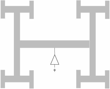
42 Capacitance Crosstalk V DD Capacitive coupling introduces crosstalk. In 1 In 2 In 3 φ φ PDN C XY X C X Y 5V OV Crosstalk slows down signals to static gates, can cause hard errors in storage nodes. Crosstalk can be controlled by methodological and optimization techniques. 5x5 µm Overlap: 0.35 V Interference
43 Coupling and Crosstalk Crosstalk current depends on capacitance, voltage ramp. i c w1 w2 t C c
44 Crosstalk Analysis Assume worst-case voltage swings, signal slopes. Measure coupling capacitance based on geometrical alignment/overlap. Some nodes are particularly sensitive to crosstalk: dynamic; asynchronous.
45 Coupling Situations bus[0] sig1 a x r better bus[1] bus[2] worse
46 Layer-to-layer Coupling Long parallel runs on adjacent layers are also bad. SiO 2 siga bus[0]
47 Methodological Solutions Add ground wires between signal wires: coupling to V SS, a stable signal, dominates; can use V SS to distribute power, so long as power line is relatively stable. Extreme case add ground plane. Costs an entire layer, may be overkill.
48 Ground Wires V SS sig1 V SS sig2 V SS
49 Crosstalk and Signal Routing Can route wires to minimize required adjacency regions. Take advantage of natural holes in routing areas to decouple signals. Minimizes need for ground signals.
50 Crosstalk routing example Channel:
51 Assumptions Take into account coupling only to wires in adjacent tracks. Ignore coupling of vertical wires. Assume that coupling/crosstalk is proportional to adjacency length.

52 Bad routing

53 Good routing
54 Multi-level Interconnection
55 The Lumped Model V out Driver c wi re R driver V out V in C lumped
56 Versions of Lumped Model A driver doesn t see the total R or C of the wire. Versions of lumped model were used as good approximations. L model T model π model
57 Importance of Resistance Delay of wire to the resistance of the wire. Resistance means ohmic (IR) drop along the wire, reduces noise margin. IR drop a significant problem in the power lines where current density if high. Keep wires short, to reduce resistance. Contact resistance makes them vulnerable to electromigration.
58 How to Reduce Resistance? Materials with low resistivity (Cu). Reduce wire length not always possible. Increase width increases area and capacitance. Increase height increases fringe capacitance. Provide bigger contacts, use less vias. Use metal instead of polysilicon even for short distance routing. Use silicide coating to reduce polysilicon resistance.
59 Accurate Estimate of Cap Accurate estimate of capacitance can be done for any geometry by using field solvers. Electric fields can be solved in 2D or 3D to accurately estimate the capacitance. Example field solver FASTCAP Output usually being a capacitance matrix.
60 Estimate C Early in Design Cycle Imperative to estimate wire delay. Electric fields attenuate very fast. To calculate capacitance consider only near neighbors (both axes) A table of capacitance to ground per unit length for a given width can be created. Capacitance with horizontal neighbors depends on wire spacing.
61 Importance of Capacitance Delay of the wire is proportional to the capacitance charged. More capacitance means more dynamic power. Capacitance an increasing source of noise (coupling). Coupling make delay estimation hard.
62 How to Reduce Capacitance? Use low k dielectric which reduces permittivity and hence the capacitance. Increase the spacing between the wires (not always possible). Separate the two signals with a power or ground line (acting as shield). Use wire with minimum width wherever possible. (Increases resistance!)
63 Distributed model Wire can be modeled as a distributed RC line. As the number of elements increase distributed model becomes more accurate. For practical purposes wire-models with 5-10 elements are used to model the wire.
64 The Distributed RC-line
65 Step-response of RC Wire as a Function of Time and Space x= L/10 voltage (V) x = L/4 x = L/2 x= L time (nsec)
66 RC-Models
67 Driving an RC-line R s (r w,c w,l) V out V in
68 Reducing RC-delay Repeater
69 Delay in distributed RC line Elmore analyzed the distributed model and came up with the figures for delay. V in R 1 R R i-1 i-1 R i i R N-1 N-1 R N N V out C 1 C 2 C i-1 C i C N-1 C N τ N = N i= 1 R i N j= i C j = N i= 1 C i i j= 1 R j Elmore derived this equation in 1948 way before VLSI!!!
70 Elmore Delay First order time constant at node is a sum of RC components. All the upstream resistances are taken into account. Thus each node contributes to the delay. Amount of contribution is the product of the cap at the node and the amount of resistance from source to the node.
71 Generalized Elmore delay Rubinstein, Pinfield and Horowitz generalized Elmore delay This figure is derived from Digital integrated circuit a design perspective, J. Rabaey Prentice Hall
72 Inductance Early models didn t include inductance. For VDSM Designs it cannot be ignored. Distributed RC model no longer accurate. Distributed RLC model should be used. Difficult to analyze second order differential equations!!

73 LC coupling, self L and return R These figures are derived from Design of High-Performance Microprocessor Circuits, A. Chandrakasan, W. Bowhill, F. Fox, IEEE, 2001
74 Inductive noise vs. line length This figure is derived from Design of High-Performance Microprocessor Circuits, A. Chandrakasan, W. Bowhill, F. Fox, IEEE, 2001
75 Impact of signal returns on farend These figures are derived from Design of High-Performance Microprocessor Circuits, A. Chandrakasan, W. Bowhill, F. Fox, IEEE, 2001
76 Inductive Effects in Integrated Circuits Coaxial Cable Triplate Strip Line MicroStrip Wire above Ground Plane
77 Decoupling Capacitors + Board Wiring Bonding Wire SUPPLY C d CHIP - Decoupling Capacitor
78 The Transmission Line V in r l r l r l x r l V out g c g c g c g c
79 Lossless Transmission Line - Parameters speed of light in vacuum
80 Wave Propagation Speed
81 Wave Reflection for Different Terminations
82 Transmission Line Response (R L = ) V V Dest V Source R S = 5Z 0 (a) V R S = Z 0 (b) V R S = Z 0 / t (in t lightf ) (c)
83 Lattice Diagram V Source V Dest V V V V t V V V V... L/ν
84 ECL Gate Line Response V cc V cc V cc V cc R C R C R C V in V ref L=2cm V EE R B I EE Z 0 = 100Ω VEE R B I EE V EE (a) k -1.0 Vout t (nsec)
85 Output Buffer Model V DD L = 10nH Clamping Diodes V DD V in L = 5nH Z 0 = 100 V out C L = 5pF C L R L L = 10nH (a)
86 Output Buffer - Response V in Clamped C L = 5pF R L = 10kΩ Vout 0.0 Unclamped C L = 5pF R L = 100Ω Vout (b) C L = 25pF R L = 100Ω Vout t (nsec)
87 When to Consider Transmission Line Effects?
88 RI Introduced Noise V DD I φ pre R V DD - V X V I R V
89 Power and Ground Distribution V DD Logic GND (a) Finger-shaped network V DD GND GND Logic V DD (b) Network with multiple supply pins Must size wires to be able to handle current requires designing topology of V DD /V SS networks. Want to keep power network in metal requires designing planar wiring.
90 Power distribution V DD V SS Interdigitated power and ground lines
91 Power tree design Each branch must be able to supply required current to all of its subsidiary branches: I x = b x I b Trees are interdigitated to supply both sides of power supply.
92 Planar power/ground routing theorem Draw a dividing line through each cell such that all V DD terminals are on one side and all V SS terminals on the other. If floorplan places all cells with V DD on same side, there exists a routing for both V DD and V SS which does not require them to cross. V SS V DD cell V SS V DD
93 Planar routing theorem example
94 Power supply noise Variations in power supply voltage manifest themselves as noise into the logic gates. Power supply wiring resistance creates voltage variations with current surges. Voltage drops on power lines depend on dynamic behavior of circuit.
95 Tackling power supply noise Must measure current required by each block at varying times. May need to redesign power/ground network to reduce resistance at high current loads. Worst case, may have to move some activity to another clock cycle to reduce peak current.
96 Clock distribution Goals: deliver clock to all memory elements with acceptable skew; deliver clock edges with acceptable sharpness. Clocking network design is one of the greatest challenges in the design of a large chip.

97 Clock delay varies with position
98 H-tree
99 Clock distribution tree Clocks are generally distributed via wiring trees. Want to use low-resistance interconnect to minimize delay. Use multiple drivers to distribute driver requirements use optimal sizing principles to design buffers. Clock lines can create significant crosstalk.
100 Clock distribution tree example
EE115C Winter 2017 Digital Electronic Circuits. Lecture 11: Wires, Elmore Delay
 EE115C Winter 2017 Digital Electronic Circuits Lecture 11: Wires, Elmore Delay The Wire transmitters receivers schematics physical EE115C Winter 2017 2 Interconnect Impact on Chip EE115C Winter 2017 3
Interconnect-Power Dissipation in a Microprocessor
 4/2/2004 Interconnect-Power Dissipation in a Microprocessor N. Magen, A. Kolodny, U. Weiser, N. Shamir Intel corporation Technion - Israel Institute of Technology 4/2/2004 2 Interconnect-Power Definition
High Performance Signaling. Jan Rabaey
 High Performance Signaling Jan Rabaey Sources: Introduction to Digital Systems Engineering, Bill Dally, Cambridge Press, 1998. Circuits, Interconnections and Packaging for VLSI, H. Bakoglu, Addison-Wesley,
Chapter 4. Problems. 1 Chapter 4 Problem Set
 1 Chapter 4 Problem Set Chapter 4 Problems 1. [M, None, 4.x] Figure 0.1 shows a clock-distribution network. Each segment of the clock network (between the nodes) is 5 mm long, 3 µm wide, and is implemented
Lecture 13: Interconnects in CMOS Technology
 Lecture 13: Interconnects in CMOS Technology Mark McDermott Electrical and Computer Engineering The University of Texas at Austin 10/18/18 VLSI-1 Class Notes Introduction Chips are mostly made of wires
Lecture #2 Solving the Interconnect Problems in VLSI
 Lecture #2 Solving the Interconnect Problems in VLSI C.P. Ravikumar IIT Madras - C.P. Ravikumar 1 Interconnect Problems Interconnect delay has become more important than gate delays after 130nm technology
EE141-Spring 2007 Digital Integrated Circuits
 EE141-Spring 2007 Digital Integrated Circuits Lecture 22 I/O, Power Distribution dders 1 nnouncements Homework 9 has been posted Due Tu. pr. 24, 5pm Project Phase 4 (Final) Report due Mo. pr. 30, noon
Introduction to CMOS VLSI Design (E158) Lecture 9: Cell Design
 Lecture 9: Cell Design") Harris Introduction to CMOS VLSI Design (E158) Lecture 9: Cell Design David Harris Harvey Mudd College David_Harris@hmc.edu Based on EE271 developed by Mark Horowitz, Stanford University MAH E158 Lecture
Harris Introduction to CMOS VLSI Design (E158) Lecture 9: Cell Design David Harris Harvey Mudd College David_Harris@hmc.edu Based on EE271 developed by Mark Horowitz, Stanford University MAH E158 Lecture
Switching (AC) Characteristics of MOS Inverters. Prof. MacDonald
 Characteristics of MOS Inverters. Prof. MacDonald") Switching (AC) Characteristics of MOS Inverters Prof. MacDonald 1 MOS Inverters l Performance is inversely proportional to delay l Delay is time to raise (lower) voltage at nodes node voltage is changed
Switching (AC) Characteristics of MOS Inverters Prof. MacDonald 1 MOS Inverters l Performance is inversely proportional to delay l Delay is time to raise (lower) voltage at nodes node voltage is changed
Lecture 9: Cell Design Issues
 Lecture 9: Cell Design Issues MAH, AEN EE271 Lecture 9 1 Overview Reading W&E 6.3 to 6.3.6 - FPGA, Gate Array, and Std Cell design W&E 5.3 - Cell design Introduction This lecture will look at some of the
Lecture 04 CSE 40547/60547 Computing at the Nanoscale Interconnect
 Lecture 04 CSE 40547/60547 Computing at the Nanoscale Interconnect Introduction - So far, have considered transistor-based logic in the face of technology scaling - Interconnect effects are also of concern
EE434 ASIC & Digital Systems. Partha Pande School of EECS Washington State University
 EE434 ASIC & Digital Systems Partha Pande School of EECS Washington State University pande@eecs.wsu.edu Lecture 11 Physical Design Issues Interconnect Scaling Effects Dense multilayer metal increases coupling
Deep Submicron Interconnect. 0.18um vs. 013um Interconnect
 Deep Submicron Interconnect R. Dept. of ECE University of British Columbia res@ece.ubc.ca 0.18um vs. 013um Interconnect 0.18µm 5-layer Al Metal Process 0.13µm 8-layer Cu Metal Process 1 Interconnect Scaling
Microcontroller Systems. ELET 3232 Topic 13: Load Analysis
 Microcontroller Systems ELET 3232 Topic 13: Load Analysis 1 Objective To understand hardware constraints on embedded systems Define: Noise Margins Load Currents and Fanout Capacitive Loads Transmission
Digital Systems Power, Speed and Packages II CMPE 650
 Speed VLSI focuses on propagation delay, in contrast to digital systems design which focuses on switching time: A B A B rise time propagation delay Faster switching times introduce problems independent
Interconnect. Courtesy of Dr. Daehyun Dr. Dr. Shmuel and Dr.
 Interconnect Courtesy of Dr. Daehyun Lim@WSU, Dr. Harris@HMC, Dr. Shmuel Wimer@BIU and Dr. Choi@PSU http://csce.uark.edu +1 (479) 575-6043 yrpeng@uark.edu Introduction Chips are mostly made of wires called
Interconnect/Via CONCORDIA VLSI DESIGN LAB
 Interconnect/Via 1 Delay of Devices and Interconnect 2 Reduction of the feature size Increase in the influence of the interconnect delay on system performance Skew The difference in the arrival times of
EE141- Spring 2004 Digital Integrated Circuits
 EE141- Spring 2004 Digital Integrated Circuits Lecture 27 Power distribution Resistive interconnect 1 Administrative Stuff Make-up lecture on Monday 4-5:30pm Special office hours of Prof. Rabaey today
ECE 497 JS Lecture - 22 Timing & Signaling
 ECE 497 JS Lecture - 22 Timing & Signaling Spring 2004 Jose E. Schutt-Aine Electrical & Computer Engineering University of Illinois jose@emlab.uiuc.edu 1 Announcements - Signaling Techniques (4/27) - Signaling
On-Chip Inductance Modeling
 On-Chip Inductance Modeling David Blaauw Kaushik Gala ladimir Zolotov Rajendran Panda Junfeng Wang Motorola Inc., Austin TX 78729 ABSTRACT With operating frequencies approaching the gigahertz range, inductance
Microelectronics, BSc course
 Microelectronics, BSc course MOS circuits: CMOS circuits, construction http://www.eet.bme.hu/~poppe/miel/en/14-cmos.pptx http://www.eet.bme.hu The abstraction level of our study: SYSTEM + MODULE GATE CIRCUIT
Microcircuit Electrical Issues
 Microcircuit Electrical Issues Distortion The frequency at which transmitted power has dropped to 50 percent of the injected power is called the "3 db" point and is used to define the bandwidth of the
EECS 141: SPRING 98 FINAL
 University of California College of Engineering Department of Electrical Engineering and Computer Science J. M. Rabaey 511 Cory Hall TuTh3:3-5pm e141@eecs EECS 141: SPRING 98 FINAL For all problems, you
VLSI is scaling faster than number of interface pins
 High Speed Digital Signals Why Study High Speed Digital Signals Speeds of processors and signaling Doubled with last few years Already at 1-3 GHz microprocessors Early stages of terahertz Higher speeds
04/29/03 EE371 Power Delivery D. Ayers 1. VLSI Power Delivery. David Ayers
 04/29/03 EE371 Power Delivery D. Ayers 1 VLSI Power Delivery David Ayers 04/29/03 EE371 Power Delivery D. Ayers 2 Outline Die power delivery Die power goals Typical processor power grid Transistor power
Digital Integrated Circuits Lecture 20: Package, Power, Clock, and I/O
 Digital Integrated Circuits Lecture 20: Package, Power, Clock, and I/O Chih-Wei Liu VLSI Signal Processing LAB National Chiao Tung University cwliu@twins.ee.nctu.edu.tw DIC-Lec20 cwliu@twins.ee.nctu.edu.tw
Power Supply Networks: Analysis and Synthesis. What is Power Supply Noise?
 Power Supply Networs: Analysis and Synthesis What is Power Supply Noise? Problem: Degraded voltage level at the delivery point of the power/ground grid causes performance and/or functional failure Lower
FDTD SPICE Analysis of High-Speed Cells in Silicon Integrated Circuits
 FDTD Analysis of High-Speed Cells in Silicon Integrated Circuits Neven Orhanovic and Norio Matsui Applied Simulation Technology Gateway Place, Suite 8 San Jose, CA 9 {neven, matsui}@apsimtech.com Abstract
Modeling the Effect of Wire Resistance in Deep Submicron Coupled Interconnects for Accurate Crosstalk Based Net Sorting
 Modeling the Effect of Wire Resistance in Deep Submicron Coupled Interconnects for Accurate Crosstalk Based Net Sorting C. Guardiani, C. Forzan, B. Franzini, D. Pandini Adanced Research, Central R&D, DAIS,
6.776 High Speed Communication Circuits Lecture 6 MOS Transistors, Passive Components, Gain- Bandwidth Issue for Broadband Amplifiers
 6.776 High Speed Communication Circuits Lecture 6 MOS Transistors, Passive Components, Gain- Bandwidth Issue for Broadband Amplifiers Massachusetts Institute of Technology February 17, 2005 Copyright 2005
ECE 484 VLSI Digital Circuits Fall Lecture 02: Design Metrics
 ECE 484 VLSI Digital Circuits Fall 2016 Lecture 02: Design Metrics Dr. George L. Engel Adapted from slides provided by Mary Jane Irwin (PSU) [Adapted from Rabaey s Digital Integrated Circuits, 2002, J.
EE 434 ASIC and Digital Systems. Prof. Dae Hyun Kim School of Electrical Engineering and Computer Science Washington State University.
 EE 434 ASIC and Digital Systems Prof. Dae Hyun Kim School of Electrical Engineering and Computer Science Washington State University Preliminaries VLSI Design System Specification Functional Design RTL
Low Power Design in VLSI
 Low Power Design in VLSI Evolution in Power Dissipation: Why worry about power? Heat Dissipation source : arpa-esto microprocessor power dissipation DEC 21164 Computers Defined by Watts not MIPS: µwatt
IFSIN. WEB PAGE Fall ://weble.upc.es/ifsin/
 IFSIN IMPLEMENTACIÓ FÍSICA DE SISTEMES INTEGRATS NANOMÈTRICS IMPLEMENTACIÓN N FÍSICA F DE SISTEMAS INTEGRADOS NANOMÉTRICOS PHYSICAL IMPLEMENTATION OF NANOMETER INTEGRATED SYSTEMS Fall 2008 Prof. Xavier
Trends and Challenges in VLSI Technology Scaling Towards 100nm
 Trends and Challenges in VLSI Technology Scaling Towards 100nm Stefan Rusu Intel Corporation stefan.rusu@intel.com September 2001 Stefan Rusu 9/2001 2001 Intel Corp. Page 1 Agenda VLSI Technology Trends
Homework 10 posted just for practice. Office hours next week, schedule TBD. HKN review today. Your feedback is important!
 EE141 Fall 2005 Lecture 26 Memory (Cont.) Perspectives Administrative Stuff Homework 10 posted just for practice No need to turn in Office hours next week, schedule TBD. HKN review today. Your feedback
Design of the Power Delivery System for Next Generation Gigahertz Packages
 Design of the Power Delivery System for Next Generation Gigahertz Packages Madhavan Swaminathan Professor School of Electrical and Computer Engg. Packaging Research Center madhavan.swaminathan@ece.gatech.edu
Power Spring /7/05 L11 Power 1
 Power 6.884 Spring 2005 3/7/05 L11 Power 1 Lab 2 Results Pareto-Optimal Points 6.884 Spring 2005 3/7/05 L11 Power 2 Standard Projects Two basic design projects Processor variants (based on lab1&2 testrigs)
High-Performance Electrical Signaling
 High-Performance Electrical Signaling William J. Dally 1, Ming-Ju Edward Lee 1, Fu-Tai An 1, John Poulton 2, and Steve Tell 2 Abstract This paper reviews the technology of high-performance electrical signaling
Relationship Between Signal Integrity and EMC
 Relationship Between Signal Integrity and EMC Presented by Hasnain Syed Solectron USA, Inc. RTP, North Carolina Email: HasnainSyed@solectron.com 06/05/2007 Hasnain Syed 1 What is Signal Integrity (SI)?
(2) v max = (3) III. SCENARIOS OF PROCESS ADVANCE AND SIMULATION SETUP
 v max = (3) III. SCENARIOS OF PROCESS ADVANCE AND SIMULATION SETUP") Quantitative Prediction of On-chip Capacitive and Inductive Crosstalk Noise and Discussion on Wire Cross-Sectional Area Toward Inductive Crosstalk Free Interconnects Yasuhiro Ogasahara, Masanori Hashimoto,
Quantitative Prediction of On-chip Capacitive and Inductive Crosstalk Noise and Discussion on Wire Cross-Sectional Area Toward Inductive Crosstalk Free Interconnects Yasuhiro Ogasahara, Masanori Hashimoto,
PHYSICAL STRUCTURE OF CMOS INTEGRATED CIRCUITS. Dr. Mohammed M. Farag
 PHYSICAL STRUCTURE OF CMOS INTEGRATED CIRCUITS Dr. Mohammed M. Farag Outline Integrated Circuit Layers MOSFETs CMOS Layers Designing FET Arrays EE 432 VLSI Modeling and Design 2 Integrated Circuit Layers
DIGITAL INTEGRATED CIRCUITS A DESIGN PERSPECTIVE 2 N D E D I T I O N
 DIGITAL INTEGRATED CIRCUITS A DESIGN PERSPECTIVE 2 N D E D I T I O N Jan M. Rabaey, Anantha Chandrakasan, and Borivoje Nikolic CONTENTS PART I: THE FABRICS Chapter 1: Introduction (32 pages) 1.1 A Historical
PC accounts for 353 Cory will be created early next week (when the class list is completed) Discussions & Labs start in Week 3
 Discussions & Labs start in Week 3") EE141 Fall 2005 Lecture 2 Design Metrics Admin Page Everyone should have a UNIX account on Cory! This will allow you to run HSPICE! If you do not have an account, check: http://www-inst.eecs.berkeley.edu/usr/
EE141 Fall 2005 Lecture 2 Design Metrics Admin Page Everyone should have a UNIX account on Cory! This will allow you to run HSPICE! If you do not have an account, check: http://www-inst.eecs.berkeley.edu/usr/
Lecture 11: Clocking
 High Speed CMOS VLSI Design Lecture 11: Clocking (c) 1997 David Harris 1.0 Introduction We have seen that generating and distributing clocks with little skew is essential to high speed circuit design.
ASPDAC Tutorial: Power, Timing & Signal Integrity in SoC designs Section II
 ASPDAC Tutorial: Power, Timing & Signal Integrity in SoC designs Section II Strategic CAD, Intel Labs Chandler AZ eli.chiprout chiprout@intel.com Section II: Modeling, noise, timing The goals of this section
Low-Power VLSI. Seong-Ook Jung VLSI SYSTEM LAB, YONSEI University School of Electrical & Electronic Engineering
 Low-Power VLSI Seong-Ook Jung 2013. 5. 27. sjung@yonsei.ac.kr VLSI SYSTEM LAB, YONSEI University School of Electrical & Electronic Engineering Contents 1. Introduction 2. Power classification & Power performance
Signal integrity means clean
 CHIPS & CIRCUITS As you move into the deep sub-micron realm, you need new tools and techniques that will detect and remedy signal interference. Dr. Lynne Green, HyperLynx Division, Pads Software Inc The
Inductance 101: Analysis and Design Issues
 Inductance 101: Analysis and Design Issues Kaushik Gala, David Blaauw, Junfeng Wang, Vladimir Zolotov, Min Zhao Motorola Inc., Austin TX 78729 kaushik.gala@motorola.com Abstract With operating frequencies
Jack Keil Wolf Lecture. ESE 570: Digital Integrated Circuits and VLSI Fundamentals. Lecture Outline. MOSFET N-Type, P-Type.
 ESE 570: Digital Integrated Circuits and VLSI Fundamentals Jack Keil Wolf Lecture Lec 3: January 24, 2019 MOS Fabrication pt. 2: Design Rules and Layout http://www.ese.upenn.edu/about-ese/events/wolf.php
Propagation Delay, Circuit Timing & Adder Design
 Propagation Delay, Circuit Timing & Adder Design ECE 152A Winter 2012 Reading Assignment Brown and Vranesic 2 Introduction to Logic Circuits 2.9 Introduction to CAD Tools 2.9.1 Design Entry 2.9.2 Synthesis
Propagation Delay, Circuit Timing & Adder Design. ECE 152A Winter 2012
 Propagation Delay, Circuit Timing & Adder Design ECE 152A Winter 2012 Reading Assignment Brown and Vranesic 2 Introduction to Logic Circuits 2.9 Introduction to CAD Tools 2.9.1 Design Entry 2.9.2 Synthesis
Lecture #29. Moore s Law
 Lecture #29 ANNOUNCEMENTS HW#15 will be for extra credit Quiz #6 (Thursday 5/8) will include MOSFET C-V No late Projects will be accepted after Thursday 5/8 The last Coffee Hour will be held this Thursday
High-speed Serial Interface
 High-speed Serial Interface Lect. 9 Noises 1 Block diagram Where are we today? Serializer Tx Driver Channel Rx Equalizer Sampler Deserializer PLL Clock Recovery Tx Rx 2 Sampling in Rx Interface applications
if the conductance is set to zero, the equation can be written as following t 2 (4)
") 1 ECEN 720 High-Speed Links: Circuits and Systems Lab1 - Transmission Lines Objective To learn about transmission lines and time-domain reflectometer (TDR). Introduction Wires are used to transmit clocks
1 ECEN 720 High-Speed Links: Circuits and Systems Lab1 - Transmission Lines Objective To learn about transmission lines and time-domain reflectometer (TDR). Introduction Wires are used to transmit clocks
Lecture 17. Low Power Circuits and Power Delivery
 Lecture 17 Low Power Circuits and Power Delivery Computer Systems Laboratory Stanford University horowitz@stanford.edu Copyright 2007 Ron Ho and Mark Horowitz w/ slides used from David Ayers 1 Power Delivery
ECE 5745 Complex Digital ASIC Design Topic 2: CMOS Devices
 ECE 5745 Complex Digital ASIC Design Topic 2: CMOS Devices Christopher Batten School of Electrical and Computer Engineering Cornell University http://www.csl.cornell.edu/courses/ece5950 Simple Transistor
Introduction. Digital Integrated Circuits A Design Perspective. Jan M. Rabaey Anantha Chandrakasan Borivoje Nikolic. July 30, 2002
 Digital Integrated Circuits A Design Perspective Jan M. Rabaey Anantha Chandrakasan Borivoje Nikolic Introduction July 30, 2002 1 What is this book all about? Introduction to digital integrated circuits.
Lecture 4&5 CMOS Circuits
 Lecture 4&5 CMOS Circuits Xuan Silvia Zhang Washington University in St. Louis http://classes.engineering.wustl.edu/ese566/ Worst-Case V OL 2 3 Outline Combinational Logic (Delay Analysis) Sequential Circuits
Advanced Digital Design
 Advanced Digital Design Introduction & Motivation by A. Steininger and M. Delvai Vienna University of Technology Outline Challenges in Digital Design The Role of Time in the Design The Fundamental Design
ESE 570: Digital Integrated Circuits and VLSI Fundamentals
 ESE 570: Digital Integrated Circuits and VLSI Fundamentals Lec 3: January 24, 2019 MOS Fabrication pt. 2: Design Rules and Layout Penn ESE 570 Spring 2019 Khanna Jack Keil Wolf Lecture http://www.ese.upenn.edu/about-ese/events/wolf.php
Low-Power Digital CMOS Design: A Survey
 Low-Power Digital CMOS Design: A Survey Krister Landernäs June 4, 2005 Department of Computer Science and Electronics, Mälardalen University Abstract The aim of this document is to provide the reader with
Signal Integrity Design of TSV-Based 3D IC
 Signal Integrity Design of TSV-Based 3D IC October 24, 21 Joungho Kim at KAIST joungho@ee.kaist.ac.kr http://tera.kaist.ac.kr 1 Contents 1) Driving Forces of TSV based 3D IC 2) Signal Integrity Issues
EE4800 CMOS Digital IC Design & Analysis. Lecture 1 Introduction Zhuo Feng
 EE4800 CMOS Digital IC Design & Analysis Lecture 1 Introduction Zhuo Feng 1.1 Prof. Zhuo Feng Office: EERC 730 Phone: 487-3116 Email: zhuofeng@mtu.edu Class Website http://www.ece.mtu.edu/~zhuofeng/ee4800fall2010.html
I/O Design EE141. Announcements. EE141-Fall 2006 Digital Integrated Circuits. Class Material. Pads + ESD Protection.
 EE141-Fall 2006 Digital Integrated Circuits nnouncements Homework 9 due on Thursday Lecture 26 I/O 1 2 Class Material Last lecture Timing Clock distribution Today s lecture I/O Power distribution Intro
On Chip Active Decoupling Capacitors for Supply Noise Reduction for Power Gating and Dynamic Dual Vdd Circuits in Digital VLSI
 ELEN 689 606 Techniques for Layout Synthesis and Simulation in EDA Project Report On Chip Active Decoupling Capacitors for Supply Noise Reduction for Power Gating and Dynamic Dual Vdd Circuits in Digital
Low Power Design for Systems on a Chip. Tutorial Outline
 Low Power Design for Systems on a Chip Mary Jane Irwin Dept of CSE Penn State University (www.cse.psu.edu/~mji) Low Power Design for SoCs ASIC Tutorial Intro.1 Tutorial Outline Introduction and motivation
CIRCUITS. Raj Nair Donald Bennett PRENTICE HALL
 POWER INTEGRITY ANALYSIS AND MANAGEMENT I CIRCUITS Raj Nair Donald Bennett PRENTICE HALL Upper Saddle River, NJ Boston Indianapolis San Francisco New York Toronto Montreal London Munich Paris Madrid Capetown
A Simulation Study of Simultaneous Switching Noise
 A Simulation Study of Simultaneous Switching Noise Chi-Te Chen 1, Jin Zhao 2, Qinglun Chen 1 1 Intel Corporation Network Communication Group, LOC4/19, 9750 Goethe Road, Sacramento, CA 95827 Tel: 916-854-1178,
! Review: MOS IV Curves and Switch Model. ! MOS Device Layout. ! Inverter Layout. ! Gate Layout and Stick Diagrams. ! Design Rules. !
 ESE 570: Digital Integrated Circuits and VLSI Fundamentals Lec 3: January 21, 2017 MOS Fabrication pt. 2: Design Rules and Layout Lecture Outline! Review: MOS IV Curves and Switch Model! MOS Device Layout!
EECS 141: FALL 98 FINAL
 University of California College of Engineering Department of Electrical Engineering and Computer Science J. M. Rabaey 511 Cory Hall TuTh9:30-11am ee141@eecs EECS 141: FALL 98 FINAL For all problems, you
ECE 546 Introduction
 ECE 546 Introduction Spring 2018 Jose E. Schutt-Aine Electrical & Computer Engineering University of Illinois jesa@illinois.edu ECE 546 Jose Schutt Aine 1 Future System Needs and Functions Auto Digital
2009 Spring CS211 Digital Systems & Lab 1 CHAPTER 3: TECHNOLOGY (PART 2)
") 1 CHAPTER 3: IMPLEMENTATION TECHNOLOGY (PART 2) Whatwillwelearninthischapter? we learn in this 2 How transistors operate and form simple switches CMOS logic gates IC technology FPGAs and other PLDs Basic
1 CHAPTER 3: IMPLEMENTATION TECHNOLOGY (PART 2) Whatwillwelearninthischapter? we learn in this 2 How transistors operate and form simple switches CMOS logic gates IC technology FPGAs and other PLDs Basic
! MOS Device Layout. ! Inverter Layout. ! Gate Layout and Stick Diagrams. ! Design Rules. ! Standard Cells. ! CMOS Process Enhancements
 EE 570: igital Integrated Circuits and VLI Fundamentals Lec 3: January 18, 2018 MO Fabrication pt. 2: esign Rules and Layout Lecture Outline! MO evice Layout! Inverter Layout! Gate Layout and tick iagrams!
On-Chip Inductance Modeling and Analysis
 On-Chip Inductance Modeling and Analysis Kaushik Gala, ladimir Zolotov, Rajendran Panda, Brian Young, Junfeng Wang, David Blaauw Motorola Inc., Austin TX 78729 kaushik.gala@motorola.com Abstract With operating
DesignCon Full Chip Signal and Power Integrity with Silicon Substrate Effect. Norio Matsui Dileep Divekar Neven Orhanovic
 DesignCon 2004 Chip-Level Physical Design Full Chip Signal and Power Integrity with Silicon Substrate Effect Norio Matsui Dileep Divekar Neven Orhanovic Applied Simulation Technology, Inc. 408-436-9070
Analysis and Reduction of On-Chip Inductance Effects in Power Supply Grids
 Analysis and Reduction of On-Chip Inductance Effects in Power Supply Grids Woo Hyung Lee Sanjay Pant David Blaauw Department of Electrical Engineering and Computer Science {leewh, spant, blaauw}@umich.edu
VLSI Design I; A. Milenkovic 1
 CPE/EE 427, CPE 527 VLSI Design I L02: Design Metrics Department of Electrical and Computer Engineering University of Alabama in Huntsville Aleksandar Milenkovic ( www.ece.uah.edu/~milenka ) www.ece.uah.edu/~milenka/cpe527-03f
Jan M. Rabaey Anantha Chandrakasan Borivoje Nikolic. July 30, Digital EE141 Integrated Circuits 2nd Introduction
 Digital Integrated Circuits A Design Perspective Jan M. Rabaey Anantha Chandrakasan Borivoje Nikolic Introduction July 30, 2002 1 What is this book all about? Introduction to digital integrated circuits.
Lecture 0: Introduction
 Lecture 0: Introduction Introduction Integrated circuits: many transistors on one chip. Very Large Scale Integration (VLSI): bucketloads! Complementary Metal Oxide Semiconductor Fast, cheap, low power
L15: VLSI Integration and Performance Transformations
 L15: VLSI Integration and Performance Transformations Acknowledgement: Materials in this lecture are courtesy of the following sources and are used with permission. Curt Schurgers J. Rabaey, A. Chandrakasan,
Ramon Canal NCD Master MIRI. NCD Master MIRI 1
 Wattch, Hotspot, Hotleakage, McPAT http://www.eecs.harvard.edu/~dbrooks/wattch-form.html http://lava.cs.virginia.edu/hotspot http://lava.cs.virginia.edu/hotleakage http://www.hpl.hp.com/research/mcpat/
Disseny físic. Disseny en Standard Cells. Enric Pastor Rosa M. Badia Ramon Canal DM Tardor DM, Tardor
 Disseny físic Disseny en Standard Cells Enric Pastor Rosa M. Badia Ramon Canal DM Tardor 2005 DM, Tardor 2005 1 Design domains (Gajski) Structural Processor, memory ALU, registers Cell Device, gate Transistor
An Active Decoupling Capacitance Circuit for Inductive Noise Suppression in Power Supply Networks
 An Active Decoupling Capacitance Circuit for Inductive Noise Suppression in Power Supply Networks Sanjay Pant, David Blaauw University of Michigan, Ann Arbor, MI Abstract The placement of on-die decoupling
Substrate Coupling in RF Analog/Mixed Signal IC Design: A Review
 Substrate Coupling in RF Analog/Mixed Signal IC Design: A Review Ashish C Vora, Graduate Student, Rochester Institute of Technology, Rochester, NY, USA. Abstract : Digital switching noise coupled into
MICROPROCESSOR TECHNOLOGY
 MICROPROCESSOR TECHNOLOGY Assis. Prof. Hossam El-Din Moustafa Lecture 3 Ch.1 The Evolution of The Microprocessor 17-Feb-15 1 Chapter Objectives Introduce the microprocessor evolution from transistors to
Physical Design of Digital Integrated Circuits (EN0291 S40) Sherief Reda Division of Engineering, Brown University Fall 2006
 Sherief Reda Division of Engineering, Brown University Fall 2006") Physical Design of Digital Integrated Circuits (EN0291 S40) Sherief Reda Division of Engineering, Brown University Fall 2006 Lecture 01: the big picture Course objective Brief tour of IC physical design
Physical Design of Digital Integrated Circuits (EN0291 S40) Sherief Reda Division of Engineering, Brown University Fall 2006 Lecture 01: the big picture Course objective Brief tour of IC physical design
1 Digital EE141 Integrated Circuits 2nd Introduction
 Digital Integrated Circuits Introduction 1 What is this lecture about? Introduction to digital integrated circuits + low power circuits Issues in digital design The CMOS inverter Combinational logic structures
Signal Integrity Modeling and Measurement of TSV in 3D IC
 Signal Integrity Modeling and Measurement of TSV in 3D IC Joungho Kim KAIST joungho@ee.kaist.ac.kr 1 Contents 1) Introduction 2) 2.5D/3D Architectures with TSV and Interposer 3) Signal integrity, Channel
Lecture 12 Memory Circuits. Memory Architecture: Decoders. Semiconductor Memory Classification. Array-Structured Memory Architecture RWM NVRWM ROM
 Semiconductor Memory Classification Lecture 12 Memory Circuits RWM NVRWM ROM Peter Cheung Department of Electrical & Electronic Engineering Imperial College London Reading: Weste Ch 8.3.1-8.3.2, Rabaey
Preface to Third Edition Deep Submicron Digital IC Design p. 1 Introduction p. 1 Brief History of IC Industry p. 3 Review of Digital Logic Gate
 Preface to Third Edition p. xiii Deep Submicron Digital IC Design p. 1 Introduction p. 1 Brief History of IC Industry p. 3 Review of Digital Logic Gate Design p. 6 Basic Logic Functions p. 6 Implementation
Clocktree RLC Extraction with Efficient Inductance Modeling
 Clocktree RLC Extraction with Efficient Inductance Modeling Norman Chang, Shen Lin, Lei He*, O. Sam Nakagawa, and Weize Xie Hewlett-Packard Laboratories, Palo Alto, CA, USA *University of Wisconsin, Madison,
SOLIMAN A. MAHMOUD Department of Electrical Engineering, Faculty of Engineering, Cairo University, Fayoum, Egypt
 Journal of Circuits, Systems, and Computers Vol. 14, No. 4 (2005) 667 684 c World Scientific Publishing Company DIGITALLY CONTROLLED CMOS BALANCED OUTPUT TRANSCONDUCTOR AND APPLICATION TO VARIABLE GAIN
HMPP-386x Series MiniPak Surface Mount RF PIN Diodes
 HMPP-86x Series MiniPak Surface Mount RF PIN Diodes Data Sheet Description/Applications These ultra-miniature products represent the blending of Avago Technologies proven semiconductor and the latest in
Advanced Operational Amplifiers
 IsLab Analog Integrated Circuit Design OPA2-47 Advanced Operational Amplifiers כ Kyungpook National University IsLab Analog Integrated Circuit Design OPA2-1 Advanced Current Mirrors and Opamps Two-stage
PROCESS-VOLTAGE-TEMPERATURE (PVT) VARIATIONS AND STATIC TIMING ANALYSIS
 VARIATIONS AND STATIC TIMING ANALYSIS") PROCESS-VOLTAGE-TEMPERATURE (PVT) VARIATIONS AND STATIC TIMING ANALYSIS The major design challenges of ASIC design consist of microscopic issues and macroscopic issues [1]. The microscopic issues are ultra-high
PROCESS-VOLTAGE-TEMPERATURE (PVT) VARIATIONS AND STATIC TIMING ANALYSIS The major design challenges of ASIC design consist of microscopic issues and macroscopic issues [1]. The microscopic issues are ultra-high
Lecture 9: More about wires and wire models
 Lecture 9: More about wires and wire models Computer Systems Laboratory Stanford University ronho@vlsi.stanford.edu Copyright 2007 Ron Ho, Mark Horowitz EE371 Lecture 9 Spring 2006-2007 1 Introduction
Chapter 3 Novel Digital-to-Analog Converter with Gamma Correction for On-Panel Data Driver
 Chapter 3 Novel Digital-to-Analog Converter with Gamma Correction for On-Panel Data Driver 3.1 INTRODUCTION As last chapter description, we know that there is a nonlinearity relationship between luminance
Fabrication, Corner, Layout, Matching, & etc.
 Advanced Analog Building Blocks Fabrication, Corner, Layout, Matching, & etc. Wei SHEN (KIP) 1 Fabrication Steps for MOS Wei SHEN, Universität Heidelberg 2 Fabrication Steps for MOS Wei SHEN, Universität
Lecture 16. Complementary metal oxide semiconductor (CMOS) CMOS 1-1
 CMOS 1-1") Lecture 16 Complementary metal oxide semiconductor (CMOS) CMOS 1-1 Outline Complementary metal oxide semiconductor (CMOS) Inverting circuit Properties Operating points Propagation delay Power dissipation
Lecture 16 Complementary metal oxide semiconductor (CMOS) CMOS 1-1 Outline Complementary metal oxide semiconductor (CMOS) Inverting circuit Properties Operating points Propagation delay Power dissipation