Prepared By: Nida Qureshi (Lecturer) Reviewed By: Mr. Muhammad Khurram Shaikh (Assistant Professor) Approved By:
|
|
|
- Barnard Boone
- 6 years ago
- Views:
Transcription
1 LABORATORY WORK BOOK For The Course EL-335 Digital Electronics Prepared By: Nida Qureshi (Lecturer) Reviewed By: Mr. Muhammad Khurram Shaikh (Assistant Professor) Approved By: The Board of Studies of Department of Electronic Engineering
2 Introduction The work book emphasizes on the basic components of digital electronics including op-amps, analog switches, different ICs, sample-and-hold circuit, ADC and DACs. All these components are pre fabricated on experiment modules, so students do not need to assemble any thing manually. These study modules are provided with complete power supply block and different electronic components so that different circuits can be established through jumpers and connecting wires. This makes it easy to observe the circuit and more time is at its disposal for observation rather then wasting time in assembling. Apart from this students will acquire comprehensive knowledge of equipments like Digital Multimeter, Function Generator and Digital Oscilloscope. By attaining knowledge of these equipments, components and accouterments students will be capable of designing, analyzing and observing an electronic circuit.
3 Digital Electronics Laboratory CONTENTS Lab. No. Date List of Experiments Page Remarks To produce an astable multivibrator with: Symmetrical square wave output 1 Non-Symmetrical square wave output 1-5 To determine the frequency and output amplitude 2 of a triangular wave generator 6-10 To determine the frequency and output amplitude of a ramp generator 3 To illustrate the operation and characteristics of the analog switches To illustrate the switching times and switching threshold of the analog switches To illustrate the operation and characteristics of the sample and hold circuit General considerations on the Digital-to-Analog and Analog-to-Digital Conversion. And observation of its different parameters. Frequency analysis of the Digital-to-Analog and Analog-to-Digital Conversion and observation of its different Description of the module E18/EV and to illustrate the gate delay of a TTL Inverter To study the Basic Characteristics of Flip-Flops To observe the propagation and transition times of CMOS and TTL Gates To implement a) 2-bit counter circuit b) Frequency divider circuit Using JK-flip flop To implement a circuit that generates the magnitude of 2 s complement number and then compare it with another number using a magnitude comparator and start a counter when certain condition true
4 Lab No.1 PURPOSE: To produce an astable multivibrator with: Symmetrical square wave output Non-symmetrical square wave output EQUIPMENT REQUIRED: Base unit for the IPES system Experiment module MCM7/EV Digital multimeter Function generator Oscilloscope Theory: With an astable multivibrator, the op amp operates only in the non-linear region. So its output has only two voltage levels, Vmin and Vmax. The astable continually switches from one state to the other, staying in each state for a fixed length of time. The circuit of an astable multivibrator is shown in figure f7.01. Note that this circuit does not need an input signal. To find out the relations governing the operation of the astable, we start with the usual hypothesis that the operational amplifier has an ideal behavior. Suppose the output is in the state Vo = Vmax. When Vo takes this value the voltage V Al of the non inverting input is: V Al = Vmax.R 1/ (R1 + R2) The capacitor C starts charging through resistor R towards the value Vmax. This charging continues until the voltage V B of the inverting input reaches the value V Al. At this point, as the inverting input voltage is more than the non-inverting input, the output switches low, to Vmin. The voltage V A2 is now given by: V A2 = Vmin.R1 / (R1 + R2) At this point, the capacitor C starts discharging through R towards the voltage Vmin until it reaches the value V A2, at which point the output switches to Vmax.The cycle then starts again. We have seen that the voltage across the capacitor C can vary from V Al to V A2, so in the period of time when the output is low, at Vmin, the voltage on the capacitor is given by: V B (t)=vmin (Vmin-Vmax*R1/(R1 + R2))*e -t/r*c While in the period of time when the output is at Vmax, the capacitor voltage is: V B (t)=vmax (Vmax-Vmin*R1/(R1 + R2))*e -t/r*c 1
5 The period T1 for which the output voltage is at Vmax can be found by calculating the time the capacitor voltage takes to equal V Al. So: From which: Vmax/(R1+R2) = (Vmin/(R1+R2)-Vmax)*e -T1/R*C + Vmax T1=R*C*ln Vmax-R1/(R1+R2)*Vmin Vmax-R1/(R1+R2)*Vmax Similarly we can find the period T2 for which the output stays at Vmin: T2=R*C*ln Vmax*R1/(R1+R2)-Vmin Vmax*R1/ (R1+R2)-Vmin Supposing that Vmin = -Vmax we obtain: T1=T2=R*C*ln 1+R1/ (R1+R2) 1-R1/ (R1+R2) The total period T of the square-wave is given by the sum of T 1 and T2. We can see that the square-wave period and so the frequency can be varied by varying the values of R1, R2, R and C. To obtain an asymmetrical square-wave (duty cycle not 50%) we can make the capacitor charge and discharge through resistors of different values. Figure F1.1 R _ C V B + V o V A R2 R1 2
6 V MAX V MIN T 1 T 2 Symmetrical square wave V MAX V MIN T 1 T 2 Non-symmetrical square wave Procedure: Insert jumpers J3, J16, J22, J30, J34 to produce the circuit of figure F7.02 Calculate the output frequency with the formulae. Connect the first probe of the oscilloscope to the output V o of the amplifier and the second probe to the inverting input V B -Measure the frequency with the oscilloscope, and compare it with the theoretical result Calculate the capacitor voltages at which output switching occurs, according to the formulae Measure the capacitor voltages at which output switching occurs and compare the results with those calculated from theory 3
7 Figure F1.2 Figure F1.3 Now connect jumper J27, to produce the circuit of figure F7.03 Connect the first probe of the oscilloscope to the output of the A l operational amplifier and the second to the inverting input VB Calculate the values of T1 and T2 as given by the formulae. Measure the values of T1 and T2 with the oscilloscope. Observation(Symmetrical square wave): S.NO. Quantity Observed Value Calculated Value 1 V B (P-P) 2 V O(P-P) 3 Frequency 4 Vmax 5 Vmin 6 Capacitor charging time 7 Capacitor discharging time Outcome: The approximate frequency of the oscillation of the astable multivibrator (Symmetrical square wave), when R1=R2=10k and R=100K, C = 68nf and Vmin = -Vmax comes out to be: 1 / T1+T2 = 4
8 Observation(Non symmetrical square wave): S.NO. Quantity Observed Value Calculated Value 1 V B (P-P) 2 V O(P-P) 3 Frequency 4 Vmax 5 Vmin 6 Capacitor charging time 7 Capacitor discharging time Outcome: The approximate frequency of the oscillation of the astable multivibrator (Non symmetrical square wave), when R1=R2=10k and R=100K, C = 68nf and Vmin = -Vmax comes out to be: 1 / T1+T2 = 5
9 Lab No.2 PURPOSE: To determine the frequency and output amplitude of a triangular wave generator To determine the frequency and output amplitude of a ramp generator EQUIPMENT REQUIRED: Base unit for the IPES system Experiment module MCM7/EV Digital multimeter Oscilloscope Theory: Among the waveforms that can be generated with op amps, the most common are the triangular, the ramp and the square-wave. A triangular wave can be generated with the circuit of figure F8.01.in which two operational amplifiers are used. The first operates as a comparator, while the second as an integrator. V O is the output voltage of the integrator, Vr the output voltage of the comparator. The saturation voltages Vmax and Vmin are equal in amplitude, and so can be called +Vr and Vr respectively. Suppose the output of the comparator is +Vr. The voltage V O will be a negative ramp which will continue to grow until the voltage of the non-inverting input of the comparator rises above zero. The minimum value of the output voltage V O, applying the superposition principle, will be given by: 0=Vr*R3 +V O *R1 R1+R3 From which we get: V O = -Vr*R3/R1 Figure F2.1 6
10 The same principles apply for the maximum voltage the output reaches, with the only difference that the ramp is raising and the voltage Vr is negative: defining this voltage as V O ' we have: Vo' = Vr *R3 / Rl To calculate the time T taken to rise from V O to V O ' remember that the capacitor C charges with a constant current given by: I = Vr / (P+R2) So, from: I = - C*dVo / dt We find that: From which: Vr = -C* (Vo' -Vo) P+R2 T V o' -Vo = - Vr*T C*(P+R2) As: Vo' -Vo = 2*Vr*R3 / Rl we have: T = 2*R3*(P + R2)*C / Rl The time T is equal to half period, so the output frequency F will be the inverse of twice T: F = R1/ [4*R3*(R2+P)*C] Vo' Vo T 1 T 2 Triangular wave To convert the triangular wave generator to a ramp generator (also known as a saw-tooth) simply insert a diode and resistor in parallel with the potentiometer P and resistor R2. The diagram is shown in figure F2.2 7
11 Figure F2.2 Just as with the triangular wave generator, the positive ramp is generated by the current flowing through P and R2 (the diode D is reverse biased), while for the negative ramp the capacitor discharges through a smaller resistance (given by R5 in parallel with the series of P and R2) and so it is faster. So the time T1 to go from Vr*R3/Rl to +Vr*R3/Rl is the same as a triangular wave generator, while the time T2 of the return to Vr*R3/R1 is given by: T2 = 2*R3*R P *C R1 Where: R P = (P+R2) // R5 As in module MCM7 the resistance R5 is much less than the value of P and R2, R P can be considered equal to R5. With this approximation: T2=2*R3*R5*C RI With the values used in the module, and with the potentiometer all inserted, T2 = 4.4 µsec which can be neglected in comparison with T1 which is about few milliseconds. The frequency of the ramp generator is equal to: F = R1/ [2*R3*(R2+P)*C] To obtain a square wave generator, take the signal from the output of the first op amp, and if the charge and discharge times of the integrator are equal, the output voltage will be symmetrical. 8
12 Vo' Vo T 1 Procedure: Triangular waveform generator Ramp/saw tooth wave Insert jumpers J3, J13, J33, J34, J37, J39, J44, J53, J55 to the circuit of figure F2.3 Adjust RV6 completely CCW to obtain zero resistance and the output voltage value of the comparator (terminal 3) using oscilloscope. Adjust the trimmer RV6 to half value. Calculate the amplitude of the output voltage (terminal 5). Measure the amplitude of the output voltage with the oscilloscope. Calculate the output voltage frequency according to the formulae. Measure the output frequency with the oscilloscope. Check the presence of a square wave at the output of the comparator (terminal 3). Figure F2.3 Ramp generator: From previous circuit insert J36 to produce the circuit of figure F8.04. Adjust RV6 completely CCW to obtain zero resistance. Measure the amplitude of the output voltage with the oscilloscope 9
13 Calculate the output frequency using formulae Measure the output frequency with the oscilloscope Measure the charge and discharge times of the capacitor Figure F2.4 Observation: S.NO. Quantity Observed Value Calculated value 1 V O (triangular) 2 Frequency (triangular) 3 V O (Ramp) 4 Frequency (Ramp) Outcome: Triangular: The approximate frequency of the oscillation of the astable multivibrator comes out to be:. The output voltage of the oscillation of the astable multivibrator comes out to be:. Ramp: The approximate frequency of the oscillation of the astable multivibrator comes out to be:. The output voltage of the oscillation of the astable multivibrator comes out to be:. 10
14
15 Lab No.3 PURPOSE: To illustrate the operation and characteristics of the analog switches. EQUIPMENT REQUIRED: Base unit for the IPES system Experiment module G33/EV Digital multimeter Basic theory: CMOS Switches MOSFETs are easily integrated into driver circuits on a single chip, and are therefore suitable for use as analog signal switches. The main disadvantage in switches featuring PMOS and NMOS transistors is there sensitivity to ON resistance at the analog signal voltage. This problem can almost entirely eliminated by the use of CMOS switch consists of two parallel switches one featuring a channel-p MOSFET, the other with a channel-n MOSFET this parallel combination gives a relatively flat ON resistance/ analog signal voltage curve. PMOS R ON NMOS CMOS Analog Signal (V) 12
 analog switch which employs CMOS technology to ensure low and nearly constant ON resistance over the entire analog")
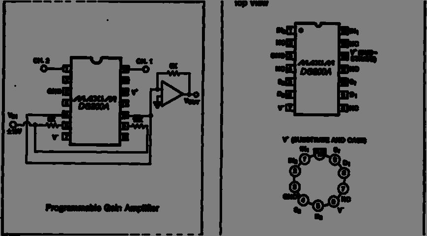
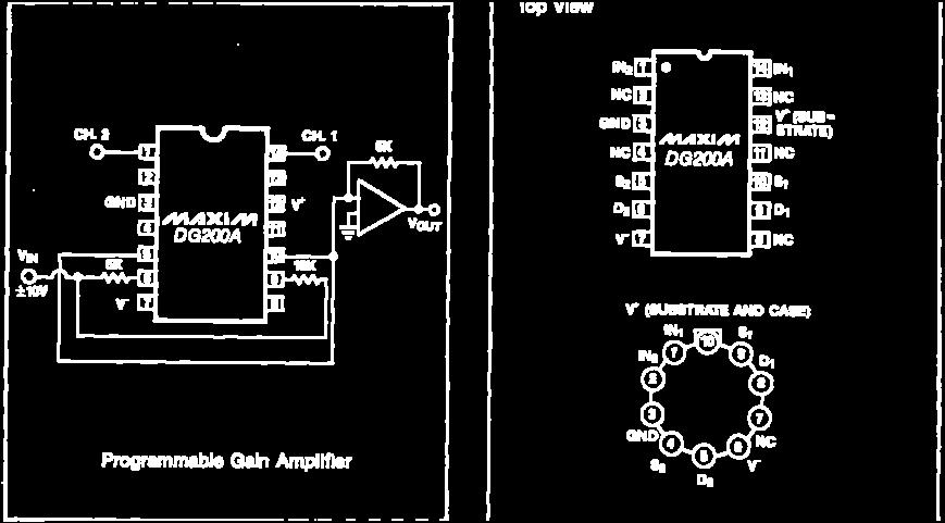
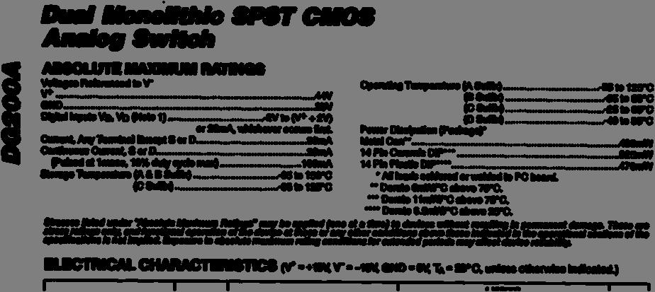
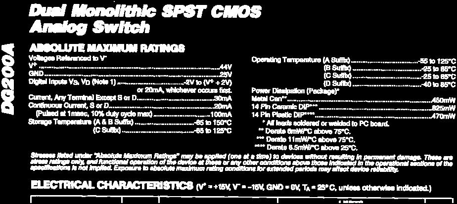
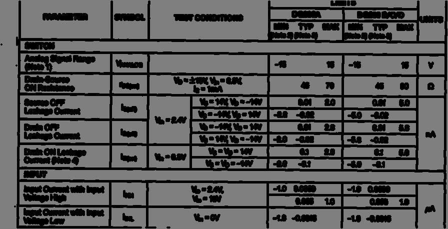
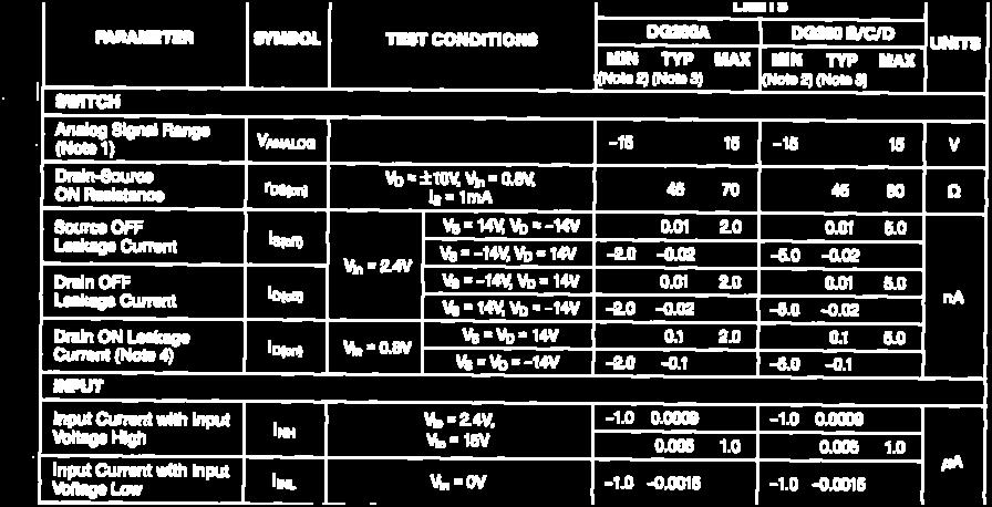
16 DESCRIPTION OF THE MODULE ANALOG SWITCH The section of the circuit denominated" ANALOG SWITCH" consists of the integrated analog switch ICs (DG 200 CJ). The data sheet shows that this is a two-channel single-pole single-throw (SPST) analog switch which employs CMOS technology to ensure low and nearly constant ON resistance over the entire analog signal range. The switch will conduct current in both directions with no offset voltage in the ON condition and block voltages up to 30 Vp-p in the OFF condition. The ON-OFF state of each switch is controlled by a driver. With logic "0" at the input to the driver, the switch will be ON; logic "1" will turn the switch OFF. A voltage of between 0 and 0.8V is required for logic "0", while logic "1" is given by a voltage of between 2.4 and 15V. The input can therefore be directly interfaced with TTL, DTL, RTL and CMOS circuits. The switch action is break-before-make, in order to prevent any shorting in the input signal. For the sake of convenience in the execution of the exercises, and as the switch is bidirectional, the two terminals of the analog switch are indicated on the trainer panel as SWITCH IN and SWITCH OUT. The driver logic input may be manual (ON/OFF operation via special switch) or external. This is selected by fitting a jumper between jack 12 and jack 14. Figure F3.1 Procedure: Measuring r DS (ON) without current Purpose of the exercise The purpose of this exercise is to measure the drain-source resistance present in the analog switch without current. Procedure Connect the ±12V and ground jacks on the panel to a corrected power supply. 13
17 Connect jack 12 to jack 14. Connect the digital multimeter (set to measure ohms) between jacks 9 and 10. Set switch I 1 to ON; read the value of r DS (ON) indicated on the digital multimeter. Measuring r DS (ON) with current Purpose of the exercise The purpose of this exercise is to measure the drain-source resistance present in the analog switch in the ON state as the current increases. Procedure Connect the ±12V and ground jacks on the panel to a corrected power supply. Connect jacks 12 and 14. Connect a variable 0 => + 12V DC power supply between jack 9 and ground. Set switch I 1 to ON. Increase the input voltage gradually until voltage can be measured at the terminals of R 26, as shown in column 1 of table 9.1. For each R 26 voltage, measure the voltage between jacks 9 and 10 and list these voltages in column Care should be taken to avoid exceeding 12V, as this might damage the unit. Given R 26 equivalent to 1.2KΩ. Calculate the current circulating between drain and source. From V DS and I DS, calculate the value of R DS and list in column 4. Plot the drain source current values (I DS - ma) on the x-axis and the drain source resistance values (R DS - Ω) on the y-axis. Table 3.1. S.N. V R26 (volts) I DS(mA) V DS (mv) R DS (Ω) Outcome: The R DS (ON) without current comes out to be: The R DS (ON) with current 2 ma comes out to be: 14

18 Lab No.4 PURPOSE: To illustrate the switching times and switching threshold of the analog switches. EQUIPMENT REQUIRED: Base unit for the IPES system Experiment module G33/EV Digital multimeter Function generator Oscilloscope Basic theory: One of the main specifications regarding the application of analog switches is the TURN ON TIME and the TURN OFF TIME. When a switch is commanded to change from ON to OFF, and vice-versa, a propagation delay occurs in the circuit driver. The T ON and T OFF times may be used to determine when a switch begins operation and whether multiple switches connected in a multiplexer configuration will be "make-before-break" or "break-before-make", i.e. whether the switches are triggered and then pause, or whether the pause precedes their action. The propagation delay should not be confused with the settling time, which is also effected by the load impedance. Two transitions will therefore apply: OFF to ON t settling = t ON + t l where t l = f (R ON, R LOAD, C D, C LOAD ) ON to OFF t settling = t OFF + t l where t l. = f (R LOAD, C LOAD, C D ) Figure F4.1 15
19 Measurement of the switching time Purpose of the exercise The purpose of this exercise is to determine the time required by the analog switch to open and close. Procedure Connect the ±12V and ground jacks on the panel to a corrected power supply. Connect a + 10V DC power supply between jack 9 and ground. Send a rectangular signal from the function generator between jack 12 and ground (amplitude 5V positive, frequency 50 KHz). Connect one of the probes of the oscilloscope to the generator signal and the other to the output signal present between jack 10 and ground. Measure the switching times between the output signal and the control signal; i.e. the rise time which corresponds to the closing of the analog switch and the fall time which corresponds to its opening. Figure F.4.2 INPUT signal OUTPUT signal T ON TOFF Measurement of the switching threshold Purpose of the exercise The purpose of this exercise is to measure the voltages at which the analog switch opens and closes. Procedure Connect the ±12V and ground jacks on the panel to a corrected power supply. Connect a +5V DC power supply between jack 9 and ground. Send a triangular signal from the function generator between the 12 jack and ground (amplitude 5V positive, frequency 1 KHz). Connect one of the probes of the oscilloscope to the generator signal and the other to the output signal present between jack 10 and ground. Measure the switching threshold by comparing the output signal with the control signal, i.e. the amplitude of the control signal at which the analog switch opens (V 1 ) and the amplitude at which it closes (V 2 ). 16
20 Figure 6.01 shows measurements carried out on a sample switch. V Figure F4.3 Signal in Signal out V 1 switch -OFF V 1 switch -ON Outcome: The t ON (Turn ON time) of the analog switch comes out to be: The t OFF (Turn OFF time) of the analog switch comes out to be: The voltages at which the analog switch opens comes out to be: The voltages at which the analog switch closes comes out to be: 17
21 Lab No.5 PURPOSE: To illustrate the operation and characteristics of the sample and hold circuit EQUIPMENT REQUIRED: Base unit for the IPES system Experiment module G33/EV Function generator Oscilloscope Theory: Introduction The most simple sample and hold circuit consists of a switch and a capacitance. Two important specifications may be easily illustrated using the basic circuit. These are the aperture time and the acquisition time. The aperture time is the delay (reaction time) between the moment in which the control logic instructs the switch to open and the moment in which the aperture actually occurs. When extremely long aperture times (in the order of milliseconds) are tolerated, a relay may be used for the switch. For aperture times of less than 100 µs, FETs or BJTs are used as switches. In variable-time systems, the input signal to the sample and hold circuit changes; the sample and hold circuit holds the last signal measured. The acquisition time is the time required by the sample and hold circuit to acquire the input signal value (within a predetermined degree of accuracy) when the control logic passes from hold to sample. Clearly, the most onerous condition is that in which the output must alter over its entire range (e.g. from + 10V to -10V and vice-versa). Fig
22 Module Description Sample and hold device featuring operational amplifiers and analog switches This circuit represents a non-inverting sample and hold with four operational amplifiers and four analog switches. Operational amplifiers IC 8 and IC 10, together with analog switches IC 9 a and IC 9 c, make up the classic sample and hold circuit. As the two analog switches must operate in opposing modes: HOLD phase: IC9a = closed IC9c = open SAMPLE phase: IC9a = open IC9c = close And as there is only one command, switch IC9b is used to carry out an inversion. Capacitor C 9 is the HOLD capacitor, and is also referred to as the "data storage capacitor". Input amplifier IC 8, configured as non-inverting, has a high input resistance and features a potentiometer for calibration of the offset voltage. Operational IC 10 is of the FET type, and therefore has a very high input resistance (being connected in a non-inverting configuration). This means that the discharge of capacitor C 9 in the HOLD phase is minimal. The circuit consisting of IC 9d and IC 11 is added in order to minimize the errors introduced by analog switch IC 9c and operational amplifier IC 10. The errors introduced by these two parts of the circuit are identical (also considering that R 42 corresponds approximately to the output resistance of operational amplifier IC 8 ) and are therefore cancelled when applied to the two differential inputs of amplifier IC 12 It is important that capacitors IC 9 and IC 10 are almost identical. By connecting jack 17 to jack 19, the SAMPLE/HOLD status may be controlled via the SAMPLE/HOLD switch. If jack 17 is connected to jack 18, the SAMPLFJHOLD status is controlled by the signal from the GENERATOR. Figure F
23 Figure F 5.03 Procedure: Measuring the acquisition time Purpose of the exercise The purpose of this exercise is to measure the time required for transformation of the input signal into an output signal (starting from the beginning of the sampling phase). Procedure Connect the ±12V and ground jacks of the panel to a corrected power supply. Connect jack 17 to jack 18. Connect jack 7 to jack 5. Set switch I 2 to 10 KHz. Adjust the duty-cycle of the potentiometer so that the sample time is 60 µsec and the hold time 10 µsec (turn the knob completely counterclockwise). Connect jack 3 to jack 15. Connect one of the probes of the oscilloscope to the output signal between jack 22 and ground. The second probe should be connected first to the sample and hold signal and then to the input signal. Fig. F5.4 shows the behavior in time of the three signals. Note the existence of a delay (acquisition time) is approximately 10 to 15µsec between the "start sampling" command signal and the settling of the output signal. 20
24 Figure F5.4 Vary the duty cycle of controlling signal (connected to jack 17), and take observations. Vary the duty cycle and take observations. Connect the jack 15 and ground to function generator (sine wave of 5V positive with 5 KHz). Vary the duty cycle of controlling signal (connected to jack 17). Observe the acquisition times for different duty cycles of sample and hold signal. Repeat the procedure with triangular wave input Outcome: The time required for transformation of the square wave input signal into an output signal comes out to be as follows: Aperture Times: Rise Time = Fall Time = Acquisition Times: Rise Time = Fall Time = 21
25 Lab No.6 PURPOSE: General considerations on the Digital-to-Analog and Analog-to-Digital Conversion. And observation of its different parameters. EQUIPMENT REQUIRED: Base unit for the IPES system Experiment module F03A Digital multimeter. Basic theory: An analog-to-digital (A/D) conversion means quantizing the amplitude of a physical quantity (e.g. a voltage) into a discrete levels class. Thus obtaining a series of digits, forming a number of a proper code. Generally the binary code and, consequently, binary numbers are used. Analog data can be obtained again through digital-to-analog (D/A) conversion. Due to the quantization, each value V of the analog signal included within the interval V i to V i+1 is always quantized at the same level N i. The interval: V i+1 to V 1 = Q, is defined as "quantum level". Another important parameter of A/D converters is the conversion time since it defines the capacity of the converter to operate the conversion of a variable signal; in fact, remember that the sequence of the quantized levels must allow the regeneration of the original analog signal. A time-variable signal can be converted into a discrete values class carrying out the sampling and holding operations. The sampling and holding operations are carried out through proper circuits called "Sample and Hold". Resolution It defines the smallest standard incremental change in. the output voltage of a DAC or the amount of input voltage change required to increment the output of an ADC between a code change and the next adjacent code change. A converter with "n" switches can divide the input in 2 n parts: the least significant increment is then 2 -n, or one least significant bit (LSB). On the contrary the Most Significant Bit carries a weight of 2-1. Resolution is applied to DACs and ADCs and may be expressed in percent of full scale or in binary bits. 22
26 Quantization error The "ideal" quantization error obtained from the ideal characteristic of the A/D converter. It is the maximum deviation of a straight line of a perfect ADC, from a transfer function. As, by its very nature, an ADC quantizes the analog input into a finite number of output codes, only an infinite resolution would exhibit zero quantizing error. The quantizing error cannot strictly be applied to a DAC; in fact, the equivalent effect is more precisely a resolution error. DESCRIPTION OF THE MODULE F03A This module carries out an educational system of analog-to-digital and digital-to-analog conversion. This system consists of two 8-bit converters of large diffusion. A signal adapter is inserted before the A/D converter. This device permits the conversion of signals coming from conditioners with output range not coinciding with the converter output. The input range is chosen by acting on the IN/OUT selector and can be from 0 to +8V with the selector down and from -8 to +8V with the selector up. The input of the digital-to-analog converter can come from the analog-to-digital converter, from the computer or from a series of switches installed on the panel. The input connection is chosen through the pushbutton (D/A INPUT SELECTOR) and displayed on the LEDS of the multiplexer. The equipment must be power supplied with regulated D.C. voltages of +12,-12V and +5V. Figure F6.01 A/D converter The A/D converter (ADCO804LCN) operates with an input range included from 0V to +5 V, that is, an input voltage of 0 V generates a digital output signal consisting of a sequence of all 0s, whereas an input voltage of +5volts generates a digital signal of all 1s. Therefore the input signal must be adapted so that the minimum value of its range can generate an output signal of all 0 and the maximum value of the range generates a digital signal of all 1. 23
27 D/A Converter The digital signal (8 bits) which must be sent to the input of the D/A converter (DACO800) can come from the A/D converter, from the computer or from a set of the 8 switches. The operational amplifier IC 1A has a gain of 0.5 and carries out a shift range of the input signal if the range -8 to +8 is selected, the operational amplifier IC 1B makes the extreme range values coincide with 0v and 5v. Range: The range of module can be selected through Range IN/OUT switch. The range can be 0v to +8v, i.e. OV = V = or -8v to +8v, i.e. Procedure: -8V = V = Set switch Range IN/OUT to 0V to 8V. Resolution measurement: Connect the ±12V, +5V and ground jacks of the panel to a corrected power supply. Select SWITCH option through D/A input selector. Set the switches (S 128 to S 1 ) to any position and note the analog voltage output through multimeter. Change the position of switch S 1 (LSB), and note the analog voltage output through multimeter. The change in voltages is equal to one resolution. Binary codes for different voltage levels: Taking resolution as voltage required for LSB change, assign the binary codes to different voltage levels, starting as OV = V = Check the assigned values to the values, observed through LEDs output. Quantization error: Apply some voltage to ADC input. Increase the input voltage to maximum value so that the output of ADC does not change. Apply maximum change in input voltage for which output shows same value as previous. The change is Quantization error, normally equal to half of the resolution. 24
28 Now set the switch Range IN/OUT to -8 V to +8 V, and repeat the procedure. Observation: Input Voltage Binary Code(0 V to +8 V) Output voltage Input Voltage Binary Code(-8 V to +8 V) Output voltage Outcome: The resolution of the ADC and DAC, for the switch Range IN/OUT position 0 V to 8 V, is. The quantization error of the ADC and DAC, for the switch Range IN/OUT position 0 V to 8 V, is. The resolution of the ADC and DAC, for the switch Range IN/OUT position -8 V to +8 V, is. The quantization error of the ADC and DAC, for the switch Range IN/OUT position -8 V to +8 V, is. 25
29 Lab No.7 PURPOSE: Frequency analysis of the Digital-to-Analog and Analog-to-Digital Conversion, and observation of its different parameters: EQUIPMENT REQUIRED: Base unit for the IPES system Experiment module F03A Digital multimeter. Function generator Oscilloscope Basic theory: A time-variable signal can be converted into a discrete values class carrying out the following operations: Sampling operations: This is conversion of continuous time into discrete time, through which the instantaneous values of the analog signal are separated. The frequency of the sampling signal must guarantee the complete regeneration of the original signal. At this point, consider the sampling theorem stating that, if B is the bandwidth of the analog signal, the minimum sampling frequency must be equal to 2 B. Therefore F 2 B Sampling frequency: Analog signal is sampled at sampling frequency. The relation between analog and digital frequencies is: Digital frequency = analog frequency / sampling frequency f= F/Fs Periodic sampling of continuous-time signal implies a mapping of the infinite frequency range for the variable F (or Ω) into a finite frequency range for the variable f(or ω). Since the highest frequency in a discrete time signal is ω = π or f = ½, it follows that, with a sampling rate F s, the corresponding highest values of F and Ω are Fmax = Fs/2 = 1/2T Ωmax = π*fs = π/t Quantization operation: This is conversion of discrete time continuous valued into a discrete time discrete valued (digital) signal. it holds a constant value during the whole conversion time of the A/D converter. Actually the sampled value is held until the next sampling. Coding: In the coding process, each discrete value is represented by a binary sequence. 26
30 Procedure: Connect the ±12V, +5V and ground jacks of the panel to a corrected power supply. Select A/D option through D/A input selector. Apply different voltage values to the analog input. Read the corresponding binary values on LEDs. Note the analog output values of the D/A converter corresponding to the different digital values and compare with the analog input value. Response to a square, triangular, sine wave: Set the selector of IN/OUT RANGE to "-8 to +8 V". Select A/D option through D/A input selector. Apply a sine wave with frequency of 1 khz and amplitude not exceeding, ±8 V, to the input. Display the signal after the double conversion on oscilloscope. Compare its wave shape, amplitude, and phase shift with those of the input signal. Repeat the test with a triangular wave and with a square one. Frequency response: Repeat the last test and increase the frequency of the input signal. Note the frequency up to which the signal reconstruction is correct. Set the selector of IN/OUT RANGE to "0 to +8 V". Check the response to a sine, triangular, and square wave, with different frequencies. Outcome: The maximum frequency of the sine wave input up to which output can be reconstructed comes out to be:. The most effected wave type by increasing frequency is:. The least effected wave type by increasing frequency is:. 27
31 Lab No.8 PURPOSE: Description of the module E18/EV and to illustrate the gate delay of a TTL Inverter: EQUIPMENT REQUIRED: Base unit for the IPES system Experiment module E18/EV Digital multimeter Function generator Oscilloscope Basic theory: DESCRIPTION OF THE MODULE The educational module E18 consists in a printed circuit on which digital logic circuits (TTL and CMOS) are mounted performing the following functions: NO. of circuits Name of circuit IC -6 Inverters 74LS input AND ports 74LS input NAND ports 74LSOO input OR ports 74LS input NOR ports 74LS input EX-OR ports 74LS86-2 TTL-CMOS and CMOS-TTL interfaces MM74C906-4 J-K Flip-Flops 74LS bit full Adder 74LS bit Shift-register 74LS95-1 Synchronous BCD counter 74LS160-1 BCD decoder and display driver 74LS segment display HDSP Sync up/down counter 74LS bit parity generator 74LS280-1 Monostable 74LS221-1 Multiplexer 74LS153-1 Demultiplexer 74LS155-1 BCD to decimal decoder 74LS42 28
32 -1 Encoder 74LS147-1 Three state buffer 74LS125-1 Latch 74LS bit comparator 74LS bit preselector PICO-D-137-AK-1-1 Clock generator (1 Hz, 10 khz) 74LS14-2 Push- buttons 4/ Switches 4/ LEDs TIL210-4 NAND ports with two CMOS inputs CD pin terminals The components are mounted to carry out the experiments more quickly especially more complex circuits. The connections between terminals of the devices are carried out by means of electrical cables and proper tubes present on the module and, electrically connected to the terminals of the integrated circuits. Each integrated circuit shows the silk screen printed logical diagram. The functions related to the IC are shown and terminals (In-Out) are indicated. Implementation of the full-adder circuit, using the module E18/EV: Full- Adder A full-adder is a combinational circuit that forms the arithmetic sum of three input bits. It consists of three inputs and two outputs. Two of the input variables, denoted by x and y, represent two significant bits to be added. The third input z, represents the carry from the previous lower significant position. Two outputs are necessary because the arithmetic sum of three binary digits ranges in value from 0 to3 and binary 2or 3 needs two digits. The binary variable S indicates the sum and C the carry. The binary variable S gives the value if the least significant bit of the sum. The binary variable C gives the output carry. Procedure: Connect the ±12V and ground jacks on the panel to a corrected power supply. Make connections as shown in fig.8.1. The connections between terminals of the devices should be carried out by electrical cables and proper tubes present on the module. Supply the required power (5V) to ICs AND OR and XOR. Connect the inputs x, y, and z to switches (SW O to SW 7 ). Connect the output C and S to LEDs (LD O to LD 9 ). Check different logics by changing switch position. 29
33 Fig.8.1 Measurement of gate delay of a TTL inverter: Gate delay: Gate delay is the time taken by an IC to respond the change in input. Procedure Connect the +12V, +5V and ground jacks on the module to a corrected power supply. Connect +5V and ground of the HEX INVERTER to a corrected power supply. Send a rectangular signal from the function generator to input of HEX INVERTER (amplitude 5V positive, frequency 50 KHz). Connect one of the probes of the oscilloscope to the generator signal and the other to the corresponding output signal of the HEX INVERTER. Measure the gate delay between the output signal and the input signal. Figure F.8.2 INPUT signal OUTPUT signal T rise T fall 30
34 Outcome: The gate delay of a TTL Inverter comes out to be: The resulting truth table of the adder circuit is as follows: x y z C S
35 Lab No.9 PURPOSE: To study the Basic Characteristics of Flip-Flops EQUIPMENT REQUIRED: Theory: Base unit for the IPES system Experiment module E18/EV Introduction The bistable multivibrator, commonly called flip- flops, are the most common form of digital memory elements. A memory element is generally a device which can store the logic state 0 or 1, called information "bit". The memory elements enable the storing of digital information for further uses. They permit to carry out complex sequential digital circuits, which took to the construction of modern calculators. R-S Flip-flop (latch) A main memory circuit can be carried out with the crossed coupling of two NAND ports: this kind of connection is called R-S flip- flop. Fig. 9.1 a) shows the diagram carried out with NAND ports, while fig.9.1 b) shows the symbol. Similarly, to carry out the same flip- flop, it is also possible to use some NOR ports. TRUTH TABLE OF THE R-S FLIP FLOP X= Last state?= indefinite state S R Q Q` 0 0 X X ?? S Q R-S R Q` Fig
36 Suppose a data is to be inserted in the flip- flop; the input levels are: SET = 1 and RESET = O. The output level of the port 1 is low (0) and this determines a high state across the output of port 3 (Q = 1). The output of port 2 is instead at 1, so port 4 finds two high levels (port 2 and 3) across its inputs, and takes its output to a low level (Q = 0). The flip- flop is now on SET, with memorized information. Now, applying a high level across the RESET terminal, keeping the SET to a low level (s = 0 and R = 1), the flip- flop switches, i.e. it changes state, and the output becomes Q = 0 and Q = 1. In this case we say that the flip-flop is in RESET state. If the inputs SET and RESET are simultaneously applied to a high logic level (S = R = 1), you obtain an indeterminate state: Q=Q`=1. When the still state (R=S=O) is reset, the output having the lower transition time is taken high. R-S Flip-flop with Clock In sequential systems, the change of state in the flip-flops is often required to occur in synchronism with the clock pulse. This is carried out by modifying the diagram of fig.9.1 into the one of fig S Q R-S R Q` CK Fig. 9.2 While no input pulse is applied, the flip- flop keeps as it is, independently from the value of Rand S. Applying a clock pulse, if the inputs are R=S=O, the flip- flop keeps stable with the last output (Qn+1 = Qn). If instead we have: R = 0 and S = 1 the output of port 1 goes to 0 enabling the switching. In correspondence to a new clock pulse, if: R=1 and S=O, the latch changes state again and its outputs are: Q=O and Q=1. In the case in which: R=S=1 on arrival of the clock pulse, the outputs of the flip- flops should both go to 1. J-K flip-flop The J-K flip- flop is formed by the R-S with clock, in which the outputs are taken back to the input, as in fig
37 J Q CK K Q` Fig. 9.3 Suppose that the flip- flop is in the state: Q = 0; Q = 1. If the data input J is at the level 1 in correspondence to the clock pulse, the output of port 1 gets to 0, and the memory cell composed by ports 3-4 changes state: Q = 1 and Q = 0 This flip-flop enables the removal of the uncertainty there was in the flip- flops R-S with clock, when the inputs were both at level 1. In fact, if: Q=1 Q =O J=K=1 on arrival of the clock pulse, only port 2 enables the passage of the input data, while port 1 blocks them. The level 0 obtained across the output of port 2 makes the memory element switch (port 3 and 4). So, we ha ve seen that when the inputs are both high there is no uncertainty, but the output state changes. J-K Master-Slave Flip-flop In the J-K flip- flops there can be possibility of uncertainty, if the clock pulse duration is too long in respect to the propagation times. Considering that the flip- flop is in the following conditions: Q=O Q =1 J=K=1 When the clock pulse is applied, after the propagation time "t" of the ports, the output becomes: Q = 1 and Q = 0 But being all the inputs signals still active, the outputs would tend to oscillate between 0 and 1, and at the end of the pulse, the state of the flip- flop is uncertain. To solve this inconvenience, the flip-flop type J-K Master-Slave has been introduced, which is commonly called J-K and can be seen in fig
38 It consists in a cascade connection of two R-S flip-flops, with reaction from the output of the second one, called SLAVE, to the input of the first, and called MASTER. Some pulses inverted in respect to the ones applied to the Master are applied across the input of the Slave. If the PRESET and CLEAR inputs are not active (Pr=Cr=1), on arrival of the clock pulse, the Master can change logic state according to the following truth table: Pr = Cr = 1 t n t n+1 J K Q n Q n Q n As, during the period in which the clock pulse is high, the Slave keeps blocked, the outputs Q and Q` are not changed. When the clock passes from 1 to 0, the Slave switches, and the Master blocks. In other words, the data present across J and K are transferred first to the Master, during the positive part of the clock pulse, and then to the Slave, during the negative part: in this way, the uncertainties across the outputs are removed. D Flip-flop If a J-K flip-flop is modified by adding an inverter (as shown in fig.9.5 a), so that the input K is complement of J, the set is known as flip- flop type D, in which D=DATA (fig.9.5 b). Its operation is simple: when a clock pulse arrives, the data present across the input is transferred and kept across the output. Pr Pr D J Q Q D CK CK 1 K Q` Q` Cr Fig. 9.5 Cr T Flip-flop If the inputs J and K are set always at logic level 1 on a flip- flop J-K, so this is a flip- flop commonly called type T (T means TOGGLE).It inverts the state of the outputs each time the input pulse applied to line T passes from the state 1 to the state O. Fig.9.6 shows the diagram (a) and the logic symbol (b) of a flip- flop type T. 35
39 1 Pr Pr J Q Q CK K Q` CK T Q` Cr Fig. 9.5 Cr Procedure : Analysis of an R-S Flip-flop Procedure Carry out a flip- flop type R-S using NAND and NOT ports, as in fig.9.1 Connect the SET and RESET inputs to two switches. Connect the outputs Q and Q to two LEDs. Power the module. Turn the SET input, with the switch, to 1 and then to 0. Analyze the behavior of the outputs. Set the RESET line to 1, and then to 0. Analyze the behavior of the outputs again. Repeat some times the operations with the switches and check the carried out memorizations. Now, try to set both inputs to 1 and explain what the reason of the uncertain state is. S R Q Q` Construction and Analysis of a J-K Flip-flop Procedure Carry out the circuit of a J-K flip- flop as in fig Connect the inputs J and K to two switches, and the outputs to two LEDs. Connect the terminal of the clock at the bottom on the left to the input CK of the built up flip- flop, as well as to a led, to display the behavior. Power the module., Set the switches connected to the inputs alternatively high. : 36
40 Analyze the behavior of the LEDs. Now, set both switches to the logic level 1, and explain the behavior of the flip-flop. Comparison between J-K and J-K Master Slave Flip-flop Keep the circuit of the last exercise. Connect the switch of the input J also to J of an integrated flip-flop J-K (Master- Slave) present on the module. Carry out the same connection also for the inputs K and CK. Connect the outputs of the new flip- flops to other 2 LEDs. Power the module. Set the switches alternatively high and detect the differences between the two devices. Now, set both switches to 1 and analyze the behavior of the new flip- flop. t n t n+1 J K Q n Checking the Operation of a Flip-flop D Carry out the circuit of fig. 9.5 a) of a flip-flop type D by means of J-K flip- flops Connect the inputs P and R to 1. Check the operation of the flip- flop D by means of switches 0-1 of the input D and the Clock. t n t n+1 D Q n+1 Checking the Operation of a Flip-flop T Carry out the circuit of fig. 9.6 a) of a flip-flop type T by means of J-K flip-flop Connect the inputs P and R to 1. Check the operation of the flip- flop T by means of switches 0-1 to the Clock input. t n t n+1 T Q n+1 37
41 Lab No.10 PURPOSE: To observe the propagation and transition times of CMOS and TTL gates: EQUIPMENT REQUIRED: Module mod.e05a Power supply unit (+5 V and ±12 V) Dual trace oscilloscope Function generator Theory: Introduction Propagation delay times The following values are normally specified by the manufacturers for any log1c gate: a) t PHL : propagation delay time with output changing to the low level. b) t PLH : propagation delay time with output changing to the high level. The propagation delay times must be measured inside the fixed threshold values, which for the most part is the 50% of the whole signal varia tion. Transition times The following transition times are normally declared by the manufacturer: a) t THL : transition time with output changing to the low level. b) t TLH : transition time with output changing to the high level. The time measurement is between the 10% and the 90% of the whole signal variation. Fig shows the propagation delay time and the transition time of an inverting gate. Figure
42 Procedure : Figure 10.2 Assemble the circuit of figure 10.2 with CMOS gates: Set the function generator for a 0-12V square wave and a frequency of 1 MHz. Connect the module to the power supply (+12V). Connect one of the CMOS gate input to the function generator output and the other one to the positive of the power supply input. NOTE: Connect the input signal to the devices only when the func tion generator is ON, after the input signal has been correctly set and the device itself has been powered. Connect the gate output to the first input of the oscilloscope. Connect the output of the first gate to another CMOS gate input and to the second input of the oscilloscope. Superimpose the present signals and find the output signal delay time in respect to the input one, fo r 1 to 0 and 0 to 1 transitions. Measure the 0 to 1 and the 1 to 0 transition, times considering the voltages equal to 10% and 90% of the signal maximum; Repeat the procedure with TTL gate. Compare the speed of the devices, with other families. 39
43 Outcome: The t PHL of CMOS gates comes out to be: The t PLH of CMOS gates comes out to be: The t THL of CMOS gates comes out to be: The t TLH of CMOS gates comes out to be: The t PHL of TTL gates comes out to be: The t PLH of TTL gates comes out to be: The t THL of TTL gates comes out to be: The t TLH of TTL gates comes out to be: 40
44 LAB NO. 11 PURPOSE: To implement a) 2-bit counter circuit b) Frequency divider circuit Using JK-Flip-Flop EQUIPMENT REQUIRED: Base unit for IPES system Experiment module E18/EV Oscilloscope THEORY: Counters are digital integrated devices which can state in a well-defined sequence, applying a train pulse across the input. They are carried out with flip-flop and logic port stages, where each stage supplies an output which, together with the others, indicate the number of pulses received in binary form. clk Q0 Q1 J Q J Q K Q K Q Fig-1 1 These counters are also called BINARY COUNTERS and can be used apart as counters as frequency dividers, supplying the o/p with a pulse after n input pulses. 41
45 If we apply a fixed frequency pulse train to a counter, rather than individual pulses coming at random intervals, we begin to notice some interesting characteristics and useful relationships between the input clock signal ad the output signal. Q Consider a single flip flop with a continuous succession of clock pulses at a fixed frequency, such as the one shown above. We note three useful facts about the output signals seen at Q and Q : a) They are exactly inverted to each other b) They are perfect square waves (50% duty cycle) c) They have a frequency just half that of the clock pulse train The duty cycle of any rectangular waveform refers to the percentage of the full cycle that the signal remains at logic 1. If the signal spends half its time at logic 1 and the other half at logic 0, we have a waveform with a 50% duty cycle. This describes a perfect, symmetrical square wave. Frequency division by an odd number is also possible. The circuit shown below is a demonstration of a divide-by-3 counter. No gates are required to control the sequence if JK-flip flops are used; feeding the output signals back to the appropriate inputs is sufficient. 42
46 1 Q0 Q1 clk J K Q J Q K Q Q Fig- Of course it is not possible to get a symmetrical (50% duty cycle) square wave with this circuit. Q0 is at logic 1 for two clock pulses out of three; Q1 is at logic 1 for one clock pulse out of 3. Thus duty cycle of 1/3 (33.33%) and 2/3 (66.67%) are available. Other counting sequences are also possible. If a need exist to have two or more signals in a particular frequency relationship with each other, some extension or variation on the circuits shown can be designed to meet the need. PROCEDURE: a) 2-bit Asynchronous Counter: Carry out the circuit of Fig-1, a 2-stage asynchronous counter Connect all inputs, J and K to logic 1 (i.e +5V) Connect 1Hz clock to input CK of first flip-flop Connect Q0 to CK of second flip-flop Connect the two outputs, Q0 and Q1, to decoder/driver Connect the outputs of decoder/driver to respective inputs of display Power the module and analyze the operation of complete system b) Frequency Divider Carry out the circuit of Fig-2 Connect the CK (clock) input of both flip-flops to external 1Hz clock Connect both the K input to Q1 Connect Q0 to J input of second flip-flop Connect J-input of first flip-flop to logic 1 (+5V) Connect first channel of oscilloscope to clock input and second to Q0 Now disconnect second channel and connect it to Q1 Observe the frequencies of Q0 and Q1 with respect to input clock frequency 43
47 OUTCOME: The output frequency at Q0 =. The output frequency at Q1 =. 44
48 LAB NO. 12 PURPOSE: To implement a circuit complement number and then compare it with another number using a magnitude comparator and start a counter when certain condition true. EQUIPMENT REQUIRED: Base unit the IPES system Experiment module E18/EV THEORY: A comparator compares two binary numbers and produces an output to show if the two numbers are equal, or if one is higher than other. Ai Bi A<B < A=B = < = > Ai Bi A< B A= B A> B
49 The counter used is a synchronous BCD counter, in a synchronous counter all flip-flop stages changes state contemporarily to the arrival of the clock pulse. A higher operating speed can be reached, so that they are more largely used in industrial applications. We represent negative numbers by putting the symbol "-" in front of number. But a computer doesn t have it so easy. All it knows is bits, so we need to find some way to encode a negative number into a bit pattern so that the computer knows it s a negative value. Several schemes have been used over the years: 1) Sign and magnitude 2) 1 s complement 3) 2 s complement If we use binary comparator for numbers in sign magnitude, 1 s or 2 s complement representation, the result isn t correct. It is caused by sign bit, which is equal 1 for negative numbers but in binary numbers has the biggest weight. To obtain correct result the negative numbers should be complemented (in 1 s and 2 s complement representation), or both numbers should be tested like during addition (in sign magnitude representation). Therefore, we have to find out the magnitude for 2 s complemented 3-bit numbers in order to compare it with other binary number, to construct a circuit which will calculate the magnitude we have to find out the logic equation of the output using the following table(a,b,c are inputs and D,E are the outputs) A B C D E X X For designing the logic circuit we are neglecting the -4 value. 46
50 The simplified logic equations for obtaining two bit magnitude are: D = A B + A [B C + BC ] E = C PROCEDURE: Implement the equations to generate two bit magnitude of the 3-bit 2 s complemented number using the negative gates and switches. Connect the signal D and E to the A1 and A0 respectively of comparator s input. Connect the B1 and B0 input to the switches. Connect the comparators inputs A2, A3 B2, and B3 to ground. Connect the RES of counter to the A>B output of the comparator Connect the input CK of counter to clock of 1 Hz. Connect both the enablers EN to logic level high. Connect the outputs QA QB QC QD respectively to the LEDs. Observe the counter s output. OUTCOME 47


51 ADC0801/ADC0802/ADC0803/ADC0804/ADC Bit µp Compatible A/D Converters General Description The ADC0801, ADC0802, ADC0803, ADC0804 and ADC0805 are CMOS 8-bit successive approximation A/D converters that use a differential potentiometric ladder similar to the 256R products. These converters are designed to allow operation with the NSC800 and INS8080A derivative control bus with TRI-STATE output latches directly driving the data bus. These A/Ds appear like memory locations or I/O ports to the microprocessor and no interfacing logic is needed. Differential analog voltage inputs allow increasing the common-mode rejection and offsetting the analog zero input voltage value. In addition, the voltage reference input can be adjusted to allow encoding any smaller analog voltage span to the full 8 bits of resolution. Features n Compatible with 8080 µp derivatives no interfacing logic needed - access time ns n Easy interface to all microprocessors, or operates stand alone Connection Diagram Ordering Information November 1999 n Differential analog voltage inputs n Logic inputs and outputs meet both MOS and TTL voltage level specifications n Works with 2.5V (LM336) voltage reference n On-chip clock generator n 0V to 5V analog input voltage range with single 5V supply n No zero adjust required n 0.3" standard width 20-pin DIP package n 20-pin molded chip carrier or small outline package n Operates ratiometrically or with 5 V DC, 2.5 V DC, or analog span adjusted voltage reference Key Specifications ADC080X Dual-In-Line and Small Outline (SO) Packages n Resolution 8 bits n Total error ± 1 4 LSB, ± 1 2 LSB and ±1 LSB n Conversion time 100 µs DS See Ordering Information TEMP RANGE 0 C TO 70 C 0 C TO 70 C 40 C TO +85 C ± 1 4 Bit Adjusted ADC0801LCN ERROR ± 1 2 Bit Unadjusted ADC0802LCWM ADC0802LCN ± 1 2 Bit Adjusted ADC0803LCN ±1Bit Unadjusted ADC0804LCWM ADC0804LCN ADC0805LCN/ADC0804LCJ PACKAGE OUTLINE M20B Small Outline N20A Molded DIP ADC0801/ADC0802/ADC0803/ADC0804/ADC Bit µp Compatible A/D Converters Z-80 is a registered trademark of Zilog Corp National Semiconductor Corporation DS
52


 (No Adjustments) Adjusted ± 1 4")
53 ADC0801/ADC0802/ADC0803/ADC0804/ADC0805 Typical Applications 8080 Interface DS DS Part Number ADC0801 ADC0802 ADC0803 ADC0804 ADC0805 Error Specification (Includes Full-Scale, Zero Error, and Non-Linearity) Full- V REF /2=2.500 V DC V REF /2=No Connection Scale (No Adjustments) (No Adjustments) Adjusted ± 1 4 LSB ± 1 2 LSB ± 1 2 LSB ±1 LSB ±1 LSB 2
54 Absolute Maximum Ratings (Notes 1, 2) Infrared (15 seconds) 220 C If Military/Aerospace specified devices are required, Storage Temperature Range 65 C to +150 C please contact the National Semiconductor Sales Office/ Package Dissipation at T A =25 C 875 mw Distributors for availability and specifications. ESD Susceptibility (Note 10) 800V Supply Voltage (V CC ) (Note 3) 6.5V Voltage Operating Ratings (Notes 1, 2) Logic Control Inputs 0.3V to +18V Temperature Range T MIN T A T MAX At Other Input and Outputs 0.3V to (V CC +0.3V) ADC0804LCJ 40 C T A +85 C Lead Temp. (Soldering, 10 seconds) ADC0801/02/03/05LCN 40 C T A +85 C Dual-In-Line Package (plastic) 260 C ADC0804LCN 0 C T A +70 C Dual-In-Line Package (ceramic) 300 C ADC0802/04LCWM 0 C T A +70 C Surface Mount Package Range of V CC 4.5 V DC to 6.3 V DC Vapor Phase (60 seconds) 215 C Electrical Characteristics The following specifications apply for V CC =5 V DC, T MIN T A T MAX and f CLK =640 khz unless otherwise specified. Parameter Conditions Min Typ Max Units ADC0801: Total Adjusted Error (Note 8) With Full-Scale Adj. (See Section 2.5.2) ± 1 4 LSB ADC0802: Total Unadjusted Error (Note 8) V REF /2=2.500 V DC ± 1 2 LSB ADC0803: Total Adjusted Error (Note 8) With Full-Scale Adj. (See Section 2.5.2) ± 1 2 LSB ADC0804: Total Unadjusted Error (Note 8) V REF /2=2.500 V DC ±1 LSB ADC0805: Total Unadjusted Error (Note 8) V REF /2-No Connection ±1 LSB V REF /2 Input Resistance (Pin 9) ADC0801/02/03/05 ADC0804 (Note 9) kω kω ADC0801/ADC0802/ADC0803/ADC0804/ADC0805 Analog Input Voltage Range (Note 4) V(+) or V( ) Gnd 0.05 V CC V DC DC Common-Mode Error Over Analog Input Voltage ±1/16 ± 1 8 LSB Range Power Supply Sensitivity V CC =5 V DC ±10% Over Allowed V IN (+) and V IN ( ) Voltage Range (Note 4) ±1/16 ± 1 8 LSB AC Electrical Characteristics The following specifications apply for V CC =5 V DC and T MIN T A T MAX unless otherwise specified. Symbol Parameter Conditions Min Typ Max Units T C Conversion Time f CLK =640 khz (Note 6) µs T C Conversion Time (Notes 5, 6) /f CLK Clock Frequency V CC =5V, (Note 5) khz f CLK CR Clock Duty Cycle Conversion Rate in Free-Running Mode INTR tied to WR with CS =0 V DC, f CLK =640 khz % conv/s t W(WR)L Width of WR Input (Start Pulse Width) CS =0 V DC (Note 7) 100 ns t ACC t 1H, t 0H t WI, t RI C IN Access Time (Delay from Falling Edge of RD to Output Data Valid) TRI-STATE Control (Delay from Rising Edge of RD to Hi-Z State) Delay from Falling Edge of WR or RD to Reset of INTR Input Capacitance of Logic Control Inputs C L =100 pf ns C L =10 pf, R L =10k (See TRI-STATE Test Circuits) ns ns pf 3
55 ADC0801/ADC0802/ADC0803/ADC0804/ADC0805 AC Electrical Characteristics (Continued) The following specifications apply for V CC =5 V DC and T MIN T A T MAX unless otherwise specified. Symbol Parameter Conditions Min Typ Max Units C OUT TRI-STATE Output pf Capacitance (Data Buffers) CONTROL INPUTS [Note: CLK IN (Pin 4) is the input of a Schmitt trigger circuit and is therefore specified separately] V IN (1) Logical 1 Input Voltage V CC =5.25 V DC V DC (Except Pin 4 CLK IN) V IN (0) Logical 0 Input Voltage (Except Pin 4 CLK IN) V CC =4.75 V DC 0.8 V DC I IN (1) Logical 1 Input Current (All Inputs) V IN =5 V DC µa DC I IN (0) Logical 0 Input Current (All Inputs) V IN =0 V DC µa DC CLOCK IN AND CLOCK R V T + CLK IN (Pin 4) Positive Going V DC Threshold Voltage V T CLK IN (Pin 4) Negative Going Threshold Voltage V DC V H CLK IN (Pin 4) Hysteresis V DC (V T +) (V T ) V OUT (0) Logical 0 CLK R Output Voltage I O =360 µa V CC =4.75 V DC 0.4 V DC V OUT (1) Logical 1 CLK R Output Voltage I O = 360 µa V CC =4.75 V DC 2.4 V DC DATA OUTPUTS AND INTR V OUT (0) Logical 0 Output Voltage Data Outputs I OUT =1.6 ma, V CC =4.75 V DC 0.4 INTR Output I OUT =1.0 ma, V CC =4.75 V DC 0.4 V DC V DC V OUT (1) Logical 1 Output Voltage I O = 360 µa, V CC =4.75 V DC 2.4 V DC V OUT (1) Logical 1 Output Voltage I O = 10 µa, V CC =4.75 V DC 4.5 V DC I OUT TRI-STATE Disabled Output V OUT =0 V DC 3 µa DC Leakage (All Data Buffers) V OUT =5 V DC 3 µa DC I SOURCE V OUT Short to Gnd, T A =25 C ma DC I SINK V OUT Short to V CC, T A =25 C ma DC POWER SUPPLY I CC Supply Current (Includes f CLK =640 khz, Ladder Current) V REF /2=NC, T A =25 C and CS =5V ADC0801/02/03/04LCJ/ ma ADC0804LCN/LCWM ma Note 1: Absolute Maximum Ratings indicate limits beyond which damage to the device may occur. DC and AC electrical specifications do not apply when operating the device beyond its specified operating conditions. Note 2: All voltages are measured with respect to Gnd, unless otherwise specified. The separate A Gnd point should always be wired to the D Gnd. Note 3: A zener diode exists, internally, from V CC to Gnd and has a typical breakdown voltage of 7 V DC. Note 4: For V IN ( ) V IN (+) the digital output code will be Two on-chip diodes are tied to each analog input (see block diagram) which will forward conduct for analog input voltages one diode drop below ground or one diode drop greater than the V CC supply. Be careful, during testing at low V CC levels (4.5V), as high level analog inputs (5V) can cause this input diode to conduct especially at elevated temperatures, and cause errors for analog inputs near full-scale. The spec allows 50 mv forward bias of either diode. This means that as long as the analog V IN does not exceed the supply voltage by more than 50 mv, the output code will be correct. To achieve an absolute 0 V DC to 5 V DC input voltage range will therefore require a minimum supply voltage of V DC over temperature variations, initial tolerance and loading. Note 5: Accuracy is guaranteed at f CLK = 640 khz. At higher clock frequencies accuracy can degrade. For lower clock frequencies, the duty cycle limits can be extended so long as the minimum clock high time interval or minimum clock low time interval is no less than 275 ns. Note 6: With an asynchronous start pulse, up to 8 clock periods may be required before the internal clock phases are proper to start the conversion process. The start request is internally latched, see Figure 4 and section


56 AC Electrical Characteristics (Continued) Note 7: The CS input is assumed to bracket the WR strobe input and therefore timing is dependent on the WR pulse width. An arbitrarily wide pulse width will hold the converter in a reset mode and the start of conversion is initiated by the low to high transition of the WR pulse (see timing diagrams). Note 8: None of these A/Ds requires a zero adjust (see section 2.5.1). To obtain zero code at other analog input voltages see section 2.5 and Figure 7. Note 9: The V REF /2 pin is the center point of a two-resistor divider connected from V CC to ground. In all versions of the ADC0801, ADC0802, ADC0803, and ADC0805, and in the ADC0804LCJ, each resistor is typically 16 kω. In all versions of the ADC0804 except the ADC0804LCJ, each resistor is typically 2.2 kω. Note 10: Human body model, 100 pf discharged through a 1.5 kω resistor. Typical Performance Characteristics Logic Input Threshold Voltage vs. Supply Voltage Delay From Falling Edge of RD to Output Data Valid vs. Load Capacitance CLK IN Schmitt Trip Levels vs. Supply Voltage ADC0801/ADC0802/ADC0803/ADC0804/ADC0805 DS DS DS f CLK vs. Clock Capacitor Full-Scale Error vs Conversion Time Effect of Unadjusted Offset Error vs. V REF /2 Voltage DS DS DS Output Current vs Temperature Power Supply Current vs Temperature (Note 9) Linearity Error at Low V REF /2 Voltages DS DS DS


57 DAC0800/DAC Bit Digital-to-Analog Converters General Description The DAC0800 series are monolithic 8-bit high-speed current-output digital-to-analog converters (DAC) featuring typical settling times of 100 ns. When used as a multiplying DAC, monotonic performance over a 40 to 1 reference current range is possible. The DAC0800 series also features high compliance complementary current outputs to allow differential output voltages of 20 Vp-p with simple resistor loads as shown in Figure 1. The reference-to-full-scale current matching of better than ±1 LSB eliminates the need for full-scale trims in most applications while the nonlinearities of better than ±0.1% over temperature minimizes system error accumulations. The noise immune inputs of the DAC0800 series will accept TTL levels with the logic threshold pin, V LC, grounded. Changing the V LC potential will allow direct interface to other logic families. The performance and characteristics of the device are essentially unchanged over the full ±4.5V to ±18V power supply range; power dissipation is only 33 mw with ±5V supplies and is independent of the logic input states. Typical Applications June 1999 The DAC0800, DAC0802, DAC0800C and DAC0802C are a direct replacement for the DAC-08, DAC-08A, DAC-08C, and DAC-08H, respectively. Features n Fast settling output current: 100 ns n Full scale error: ±1 LSB n Nonlinearity over temperature: ±0.1% n Full scale current drift: ±10 ppm/ C n High output compliance: 10V to +18V n Complementary current outputs n Interface directly with TTL, CMOS, PMOS and others n 2 quadrant wide range multiplying capability n Wide power supply range: ±4.5V to ±18V n Low power consumption: 33 mw at ±5V n Low cost DAC0800/DAC Bit Digital-to-Analog Converters Ordering Information DS FIGURE 1. ±20 V P-P Output Digital-to-Analog Converter (Note 5) Non-Linearity Temperature Order Numbers Range J Package (J16A) (Note 1) N Package (N16E) (Note 1) SO Package (M16A) ±0.1% FS 0 C T A +70 C DAC0802LCJ DAC-08HQ DAC0802LCN DAC-08HP DAC0802LCM ±0.19% FS 55 C T A +125 C DAC0800LJ DAC-08Q ±0.19% FS 0 C T A +70 C DAC0800LCJ DAC-08EQ DAC0800LCN DAC-08EP DAC0800LCM Note 1: Devices may be ordered by using either order number National Semiconductor Corporation DS
58
59 DAC0800/DAC0802 Absolute Maximum Ratings (Note 2) Storage Temperature 65 C to +150 C If Military/Aerospace specified devices are required, Lead Temp. (Soldering, 10 seconds) please contact the National Semiconductor Sales Office/ Dual-In-Line Package (plastic) 260 C Distributors for availability and specifications. Dual-In-Line Package (ceramic) 300 C Supply Voltage (V + V ) ±18V or 36V Surface Mount Package Power Dissipation (Note 3) 500 mw Vapor Phase (60 seconds) 215 C Reference Input Differential Voltage Infrared (15 seconds) 220 C (V14 to V15) V to V + Reference Input Common-Mode Operating Conditions (Note 2) Range (V14, V15) V to V + Min Max Units Reference Input Current 5 ma Temperature (T A ) Logic Inputs V to V plus 36V DAC0800L C Analog Current Outputs DAC0800LC C (V S = 15V) 4.25 ma DAC0802LC C ESD Susceptibility (Note 4) TBD V Electrical Characteristics The following specifications apply for V S = ±15V, I REF = 2 ma and T MIN T A T MAX unless otherwise specified. Output characteristics refer to both I OUT and I OUT. Symbol Parameter Conditions Resolution Monotonicity Nonlinearity t s Settling Time To ± 1 2 LSB, All Bits Switched tplh, tphl Propagation Delay Each Bit All Bits Switched ON or OFF, T A =25 C DAC0800L DAC0800LC T A =25 C DAC0802LC DAC0800L/ DAC0800LC Min Typ Max Min Typ Max ± TCI FS Full Scale Tempco ±10 ±50 ±10 ±50 ppm/ C V OC Output Voltage Compliance Full Scale Current Change < 1 2 LSB, R OUT >20 MΩ Typ I FS4 Full Scale Current V REF =10.000V, R14=5.000 kω R15=5.000 kω, T A =25 C ± Units Bits Bits %FS V ma I FSS Full Scale Symmetry I FS4 I FS2 ±0.5 ±4.0 ±1 ±8.0 µa I ZS Zero Scale Current µa I FSR Output Current Range V = 5V V IL V IH I IL I IH Logic Input Levels Logic 0 Logic 1 Logic Input Current Logic 0 Logic 1 V = 8V to 18V V LC =0V V LC =0V 10V V IN +0.8V 2V V IN +18V ns ns ns ns ns ma ma 0.8 V V IS Logic Input Swing V = 15V V V THR Logic Threshold Range V S = ±15V V I 15 Reference Bias Current µa dl/dt Reference Input Slew Rate (Figure 11) ma/µs PSSI FS+ Power Supply Sensitivity 4.5V V + 18V %/% PSSI FS 4.5V V 18V I REF =1mA %/% 10 V µa µa 2


60 Electrical Characteristics (Continued) The following specifications apply for V S = ±15V, I REF = 2 ma and T MIN T A T MAX unless otherwise specified. Output characteristics refer to both I OUT and I OUT. DAC0802LC DAC0800L/ Symbol Parameter Conditions DAC0800LC Units Min Typ Max Min Typ Max Power Supply Current V S = ±5V, I REF =1 ma I ma I ma V S =5V, 15V, I REF =2 ma I ma I ma V S = ±15V, I REF =2 ma I ma I ma P D Power Dissipation ±5V, I REF =1 ma mw 5V, 15V, I REF =2 ma mw ±15V, I REF =2 ma mw DAC0800/DAC0802 Note 2: Absolute Maximum Ratings indicate limits beyond which damage to the device may occur. DC and AC electrical specifications do not apply when operating the device beyond its specified operating conditions. Note 3: The maximum junction temperature of the DAC0800 and DAC0802 is 125 C. For operating at elevated temperatures, devices in the Dual-In-Line J package must be derated based on a thermal resistance of 100 C/W, junction-to-ambient, 175 C/W for the molded Dual-In-Line N package and 100 C/W for the Small Outline M package. Note 4: Human body model, 100 pf discharged through a 1.5 kω resistor. Note 5: Pin-out numbers for the DAC080X represent the Dual-In-Line package. The Small Outline package pin-out differs from the Dual-In-Line package. Connection Diagrams Dual-In-Line Package Small Outline Package Top View DS See Ordering Information Top View DS
")


61 DAC0800/DAC0802 Block Diagram (Note 5) Typical Performance Characteristics DS Full Scale Current vs Reference Current LSB Propagation Delay vs I FS Reference Input Frequency Response DS DS DS Curve 1: C C =15 pf, V IN =2 Vp-p centered at 1V. Curve 2: C C =15 pf, V IN =50 mvp-p centered at 200 mv. Curve 3: C C =0 pf, V IN =100 mvp-p centered at 0V and applied through 50Ω connected to pin 14.2V applied to R14. Reference Amp Common-Mode Range Logic Input Current vs Input Voltage V TH V LC vs Temperature DS DS Note. Positive common-mode range is always (V+) 1.5V. DS
")


. Power Supply Current vs")


62 Typical Performance Characteristics (Continued) Output Current vs Output Voltage (Output Voltage Compliance) Output Voltage Compliance vs Temperature Bit Transfer Characteristics DAC0800/DAC0802 DS DS DS Note. B1 B8 have identical transfer characteristics. Bits are fully switched with less than 1 2 LSB error, at less than ±100 mv from actual threshold. These switching points are guaranteed to lie between 0.8 and 2V over the operating temperature range (V LC = 0V). Power Supply Current vs +V Power Supply Current vs V Power Supply Current vs Temperature Equivalent Circuit DS DS DS FIGURE 2. DS
63
64

65
66


67 LM741 Operational Amplifier General Description The LM741 series are general purpose operational amplifiers which feature improved performance over industry standards like the LM709. They are direct, plug-in replacements for the 709C, LM201, MC1439 and 748 in most applications. The amplifiers offer many features which make their application nearly foolproof: overload protection on the input and output, no latch-up when the common mode range is exceeded, as well as freedom from oscillations. August 2000 The LM741C is identical to the LM741/LM741A except that the LM741C has their performance guaranteed over a 0 C to +70 C temperature range, instead of 55 C to +125 C. LM741 Operational Amplifier Connection Diagrams Metal Can Package Dual-In-Line or S.O. Package DS Note 1: LM741H is available per JM38510/10101 Order Number LM741H, LM741H/883 (Note 1), LM741AH/883 or LM741CH See NS Package Number H08C DS Order Number LM741J, LM741J/883, LM741CN See NS Package Number J08A, M08A or N08E Ceramic Flatpak Typical Application Order Number LM741W/883 See NS Package Number W10A DS Offset Nulling Circuit DS National Semiconductor Corporation DS
68
69 LM741 Absolute Maximum Ratings (Note 2) If Military/Aerospace specified devices are required, please contact the National Semiconductor Sales Office/ Distributors for availability and specifications. (Note 7) LM741A LM741 LM741C Supply Voltage ±22V ±22V ±18V Power Dissipation (Note 3) 500 mw 500 mw 500 mw Differential Input Voltage ±30V ±30V ±30V Input Voltage (Note 4) ±15V ±15V ±15V Output Short Circuit Duration Continuous Continuous Continuous Operating Temperature Range 55 C to +125 C 55 C to +125 C 0 C to +70 C Storage Temperature Range 65 C to +150 C 65 C to +150 C 65 C to +150 C Junction Temperature 150 C 150 C 100 C Soldering Information N-Package (10 seconds) 260 C 260 C 260 C J- or H-Package (10 seconds) 300 C 300 C 300 C M-Package Vapor Phase (60 seconds) 215 C 215 C 215 C Infrared (15 seconds) 215 C 215 C 215 C See AN-450 Surface Mounting Methods and Their Effect on Product Reliability for other methods of soldering surface mount devices. ESD Tolerance (Note 8) 400V 400V 400V Electrical Characteristics (Note 5) Parameter Input Offset Voltage Average Input Offset Voltage Drift Input Offset Voltage Adjustment Range Input Offset Current Average Input Offset Current Drift Input Bias Current Input Resistance Input Voltage Range Conditions LM741A LM741 LM741C Units Min Typ Max Min Typ Max Min Typ Max T A = 25 C R S 10 kω mv R S 50Ω mv T AMIN T A T AMAX R S 50Ω 4.0 mv R S 10 kω mv 15 µv/ C T A = 25 C, V S = ±20V ±10 ±15 ±15 mv T A = 25 C na T AMIN T A T AMAX na 0.5 na/ C T A = 25 C na T AMIN T A T AMAX µa T A = 25 C, V S = ±20V MΩ T AMIN T A T AMAX, 0.5 MΩ V S = ±20V T A = 25 C ±12 ±13 V T AMIN T A T AMAX ±12 ±13 V 2
70 Electrical Characteristics (Note 5) (Continued) Parameter Conditions LM741A LM741 LM741C Units Min Typ Max Min Typ Max Min Typ Max Large Signal Voltage Gain T A = 25 C, R L 2 kω V S = ±20V, V O = ±15V 50 V/mV V S = ±15V, V O = ±10V V/mV T AMIN T A T AMAX, R L 2 kω, V S = ±20V, V O = ±15V V S = ±15V, V O = ±10V V S = ±5V, V O = ±2V Output Voltage Swing V S = ±20V R L 10 kω R L 2 kω V S = ±15V R L 10 kω R L 2 kω Output Short Circuit Current Common-Mode Rejection Ratio Supply Voltage Rejection Ratio Transient Response Rise Time Overshoot T A = 25 C T AMIN T A T AMAX T AMIN T A T AMAX R S 10 kω, V CM = ±12V 32 V/mV V/mV 10 V/mV ±16 V ±15 V ±12 ± ±14 ±13 ±12 ±10 ±14 ±13 V V ma ma db R S 50Ω, V CM = ±12V db T AMIN T A T AMAX, V S = ±20V to V S = ±5V R S 50Ω db R S 10 kω db T A = 25 C, Unity Gain µs % Bandwidth (Note 6) T A = 25 C MHz Slew Rate T A = 25 C, Unity Gain V/µs Supply Current T A = 25 C ma Power Consumption T A = 25 C V S = ±20V mw V S = ±15V mw LM741A V S = ±20V T A = T AMIN T A = T AMAX mw mw LM741 V S = ±15V T A = T AMIN T A = T AMAX mw mw LM741 Note 2: Absolute Maximum Ratings indicate limits beyond which damage to the device may occur. Operating Ratings indicate conditions for which the device is functional, but do not guarantee specific performance limits. 3

.")
 100 C/W 100 C/W 170 C/W 195 C/W θ jc (Junction to Case) N/A N/A 25")

.")
 = 0.35/Rise Time(µs).")
71 LM741 Electrical Characteristics (Note 5) (Continued) Note 3: For operation at elevated temperatures, these devices must be derated based on thermal resistance, and T j max. (listed under Absolute Maximum Ratings ). T j = T A + (θ ja P D ). Thermal Resistance Cerdip (J) DIP (N) HO8 (H) SO-8 (M) θ ja (Junction to Ambient) 100 C/W 100 C/W 170 C/W 195 C/W θ jc (Junction to Case) N/A N/A 25 C/W N/A Note 4: For supply voltages less than ±15V, the absolute maximum input voltage is equal to the supply voltage. Note 5: Unless otherwise specified, these specifications apply for V S = ±15V, 55 C T A +125 C (LM741/LM741A). For the LM741C/LM741E, these specifications are limited to 0 C T A +70 C. Note 6: Calculated value from: BW (MHz) = 0.35/Rise Time(µs). Note 7: For military specifications see RETS741X for LM741 and RETS741AX for LM741A. Note 8: Human body model, 1.5 kω in series with 100 pf. Schematic Diagram DS
")


72 Physical Dimensions inches (millimeters) unless otherwise noted LM741 Metal Can Package (H) Order Number LM741H, LM741H/883, LM741AH/883, LM741AH-MIL or LM741CH NS Package Number H08C Ceramic Dual-In-Line Package (J) Order Number LM741J/883 NS Package Number J08A 5


")

73 LM741 Physical Dimensions inches (millimeters) unless otherwise noted (Continued) Dual-In-Line Package (N) Order Number LM741CN NS Package Number N08E 10-Lead Ceramic Flatpak (W) Order Number LM741W/883, LM741WG-MPR or LM741WG/883 NS Package Number W10A 6
74
75 Notes LM741 Operational Amplifier LIFE SUPPORT POLICY NATIONAL S PRODUCTS ARE NOT AUTHORIZED FOR USE AS CRITICAL COMPONENTS IN LIFE SUPPORT DEVICES OR SYSTEMS WITHOUT THE EXPRESS WRITTEN APPROVAL OF THE PRESIDENT AND GENERAL COUNSEL OF NATIONAL SEMICONDUCTOR CORPORATION. As used herein: 1. Life support devices or systems are devices or systems which, (a) are intended for surgical implant into the body, or (b) support or sustain life, and whose failure to perform when properly used in accordance with instructions for use provided in the labeling, can be reasonably expected to result in a significant injury to the user. 2. A critical component is any component of a life support device or system whose failure to perform can be reasonably expected to cause the failure of the life support device or system, or to affect its safety or effectiveness. National Semiconductor Corporation Americas Tel: Fax: support@nsc.com National Semiconductor Europe Fax: +49 (0) europe.support@nsc.com Deutsch Tel: +49 (0) English Tel: +44 (0) Français Tel: +33 (0) National Semiconductor Asia Pacific Customer Response Group Tel: Fax: ap.support@nsc.com National Semiconductor Japan Ltd. Tel: Fax: National does not assume any responsibility for use of any circuitry described, no circuit patent licenses are implied and National reserves the right at any time without notice to change said circuitry and specifications.


76 LF198/LF298/LF398, LF198A/LF398A Monolithic Sample-and-Hold Circuits General Description The LF198/LF298/LF398 are monolithic sample-and-hold circuits which utilize BI-FET technology to obtain ultra-high dc accuracy with fast acquisition of signal and low droop rate. Operating as a unity gain follower, dc gain accuracy is 0.002% typical and acquisition time is as low as 6 µs to 0.01%. A bipolar input stage is used to achieve low offset voltage and wide bandwidth. Input offset adjust is accomplished with a single pin, and does not degrade input offset drift. The wide bandwidth allows the LF198 to be included inside the feedback loop of 1 MHz op amps without having stability problems. Input impedance of Ω allows high source impedances to be used without degrading accuracy. P-channel junction FET s are combined with bipolar devices in the output amplifier to give droop rates as low as 5 mv/min with a 1 µf hold capacitor. The JFET s have much lower noise than MOS devices used in previous designs and do not exhibit high temperature instabilities. The overall design guarantees no feed-through from input to output in the hold mode, even for input signals equal to the supply voltages. Typical Connection and Performance Curve Functional Diagram DS July 2000 Features n Operates from ±5V to ±18V supplies n Less than 10 µs acquisition time n TTL, PMOS, CMOS compatible logic input n 0.5 mv typical hold step at C h = 0.01 µf n Low input offset n 0.002% gain accuracy n Low output noise in hold mode n Input characteristics do not change during hold mode n High supply rejection ratio in sample or hold n Wide bandwidth n Space qualified, JM38510 Logic inputs on the LF198 are fully differential with low input current, allowing direct connection to TTL, PMOS, and CMOS. Differential threshold is 1.4V. The LF198 will operate from ±5V to ±18V supplies. An A version is available with tightened electrical specifications. Acquisition Time DS LF198/LF298/LF398, LF198A/LF398A Monolithic Sample-and-Hold Circuits DS National Semiconductor Corporation DS
77 LF198/LF298/LF398, LF198A/LF398A Absolute Maximum Ratings (Note 1) Hold Capacitor Short If Military/Aerospace specified devices are required, Circuit Duration 10 sec please contact the National Semiconductor Sales Office/ Lead Temperature (Note 4) Distributors for availability and specifications. H package (Soldering, 10 sec.) 260 C Supply Voltage ±18V N package (Soldering, 10 sec.) 260 C Power Dissipation (Package M package: Limitation) (Note 2) 500 mw Vapor Phase (60 sec.) 215 C Operating Ambient Temperature Range Infrared (15 sec.) 220 C LF198/LF198A 55 C to +125 C Thermal Resistance (θ JA ) (typicals) LF C to +85 C H package 215 C/W (Board mount in still air) LF398/LF398A 0 C to +70 C 85 C/W (Board mount in Storage Temperature Range 65 C to +150 C 400LF/min air flow) Input Voltage Equal to Supply Voltage N package 115 C/W Logic To Logic Reference M package 106 C/W Differential Voltage (Note 3) +7V, 30V θ JC (H package, typical) 20 C/W Output Short Circuit Duration Indefinite Electrical Characteristics The following specifcations apply for V S + 3.5V V IN +V S 3.5V, +V S = +15V, V S = 15V, T A = T j = 25 C, C h = 0.01 µf, R L = 10 kω, LOGIC REFERENCE = 0V, LOGIC HIGH = 2.5V, LOGIC LOW = 0V unless otherwise specified. Parameter Input Offset Voltage, (Note 5) Input Bias Current, (Note 5) T j = 25 C Conditions Full Temperature Range T j = 25 C Full Temperature Range LF198/LF298 LF398 Min Typ Max Min Typ Max Input Impedance T j = 25 C Ω Gain Error Feedthrough Attenuation Ratio at 1 khz Output Impedance T j = 25 C, R L = 10k Full Temperature Range T j = 25 C, C h = 0.01 µf db T j = 25 C, HOLD mode Full Temperature Range HOLD Step, (Note 6) T j = 25 C, C h = 0.01 µf, V OUT = mv Supply Current, (Note 5) T j 25 C ma Logic and Logic Reference Input Current Leakage Current into Hold Capacitor (Note 5) Acquisition Time to 0.1% T j = 25 C µa T j = 25 C, (Note 7) Hold Mode ΔV OUT = 10V, C h = 1000 pf C h = 0.01 µf 6 Units mv mv na na pa Hold Capacitor Charging Current V IN V OUT = 2V 5 5 ma Supply Voltage Rejection Ratio V OUT = db Differential Logic Threshold T j = 25 C V Input Offset Voltage, (Note 5) Input Bias Current, (Note 5) T j = 25 C Full Temperature Range T j = 25 C Full Temperature Range % % Ω Ω µs µs mv mv na na 2

 T j = 25 C, C h = 0.01µF, V OUT = 0 0.5 1 1.0 1 mv Supply Current, (Note 5) T j 25 C 4.5 5.5 4.5 6.")


78 Electrical Characteristics The following specifcations apply for V S + 3.5V V IN +V S 3.5V, +V S = +15V, V S = 15V, T A = T j = 25 C, C h = 0.01 µf, R L = 10 kω, LOGIC REFERENCE = 0V, LOGIC HIGH = 2.5V, LOGIC LOW = 0V unless otherwise specified. Parameter Conditions LF198A LF398A Units Input Impedance T j = 25 C Ω Gain Error T j = 25 C, R L = 10k % Min Typ Max Min Typ Max Full Temperature Range % Feedthrough Attenuation Ratio T j = 25 C, C h = 0.01 µf db at 1 khz Output Impedance T j = 25 C, HOLD mode Ω Full Temperature Range 4 6 Ω HOLD Step, (Note 6) T j = 25 C, C h = 0.01µF, V OUT = mv Supply Current, (Note 5) T j 25 C ma Logic and Logic Reference Input T j = 25 C µa Current Leakage Current into Hold T j = 25 C, (Note 7) pa Capacitor (Note 5) Hold Mode Acquisition Time to 0.1% ΔV OUT = 10V, C h = 1000 pf µs C h = 0.01 µf µs Hold Capacitor Charging Current V IN V OUT = 2V 5 5 ma Supply Voltage Rejection Ratio V OUT = db Differential Logic Threshold T j = 25 C V LF198/LF298/LF398, LF198A/LF398A Note 1: Absolute Maximum Ratings indicate limits beyond which damage to the device may occur. Operating Ratings indicate conditions for which the device is functional, but do not guarantee specific performance limits. Note 2: The maximum power dissipation must be derated at elevated temperatures and is dictated by T JMAX, θ JA, and the ambient temperature, T A. The maximum allowable power dissipation at any temperature is P D = (T JMAX T A )/θ JA, or the number given in the Absolute Maximum Ratings, whichever is lower. The maximum junction temperature, T JMAX, for the LF198/LF198A is 150 C; for the LF298, 115 C; and for the LF398/LF398A, 100 C. Note 3: Although the differential voltage may not exceed the limits given, the common-mode voltage on the logic pins may be equal to the supply voltages without causing damage to the circuit. For proper logic operation, however, one of the logic pins must always be at least 2V below the positive supply and 3V above the negative supply. Note 4: See AN-450 Surface Mounting Methods and their effects on Product Reliability for other methods of soldering surface mount devices. Note 5: These parameters guaranteed over a supply voltage range of ±5 to ±18V, and an input range of V S + 3.5V V IN +V S 3.5V. Note 6: Hold step is sensitive to stray capacitive coupling between input logic signals and the hold capacitor. 1 pf, for instance, will create an additional 0.5 mv step with a 5V logic swing and a 0.01µF hold capacitor. Magnitude of the hold step is inversely proportional to hold capacitor value. Note 7: Leakage current is measured at a junction temperature of 25 C. The effects of junction temperature rise due to power dissipation or elevated ambient can be calculated by doubling the 25 C value for each 11 C increase in chip temperature. Leakage is guaranteed over full input signal range. Note 8: A military RETS electrical test specification is available on request. The LF198 may also be procured to Standard Military Drawing # GA or to MIL-STD part ID JM38510/12501SGA. Typical Performance Characteristics Aperture Time (Note 9) Dielectric Absorption Error in Hold Capacitor Dynamic Sampling Error DS DS DS Note 9: See Definition of Terms 3
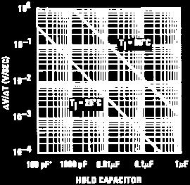
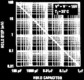
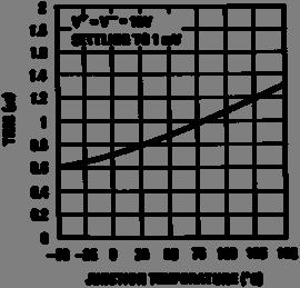
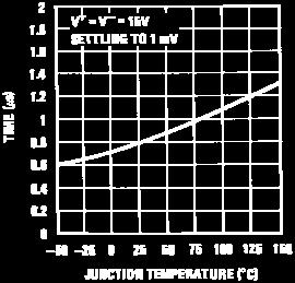
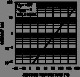
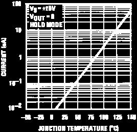
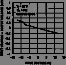
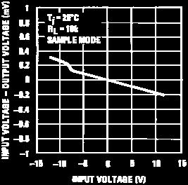
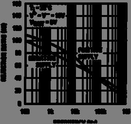
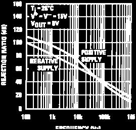
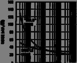
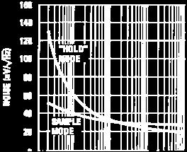
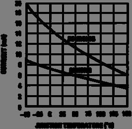
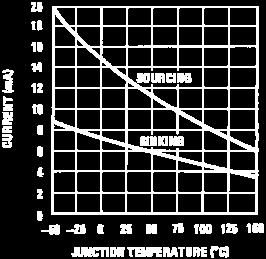
79 LF198/LF298/LF398, LF198A/LF398A Typical Performance Characteristics (Continued) Output Droop Rate Hold Step Hold Settling Time (Note 10) DS DS DS Leakage Current into Hold Capacitor Phase and Gain (Input to Output, Small Signal) Gain Error DS DS DS Power Supply Rejection Output Short Circuit Current Output Noise DS DS DS Note 10: See Definition 4
LABORATORY WORK BOOK For The Course EL-335 Digital Electronics
 LABORATORY WORK BOOK For The Course EL-335 Name : Roll No. : Batch Year Dept. : : : Department of Electronic Engineering N.E.D. University of Engineering & Technology, Karachi 75270, Pakistan LABORATORY
Module -18 Flip flops
 1 Module -18 Flip flops 1. Introduction 2. Comparison of latches and flip flops. 3. Clock the trigger signal 4. Flip flops 4.1. Level triggered flip flops SR, D and JK flip flops 4.2. Edge triggered flip
B.E. SEMESTER III (ELECTRICAL) SUBJECT CODE: X30902 Subject Name: Analog & Digital Electronics
 SUBJECT CODE: X30902 Subject Name: Analog & Digital Electronics") B.E. SEMESTER III (ELECTRICAL) SUBJECT CODE: X30902 Subject Name: Analog & Digital Electronics Sr. No. Date TITLE To From Marks Sign 1 To verify the application of op-amp as an Inverting Amplifier 2 To
B.E. SEMESTER III (ELECTRICAL) SUBJECT CODE: X30902 Subject Name: Analog & Digital Electronics Sr. No. Date TITLE To From Marks Sign 1 To verify the application of op-amp as an Inverting Amplifier 2 To
HIGH LOW Astable multivibrators HIGH LOW 1:1
 1. Multivibrators A multivibrator circuit oscillates between a HIGH state and a LOW state producing a continuous output. Astable multivibrators generally have an even 50% duty cycle, that is that 50% of
Fan in: The number of inputs of a logic gate can handle.
 Subject Code: 17333 Model Answer Page 1/ 29 Important Instructions to examiners: 1) The answers should be examined by key words and not as word-to-word as given in the model answer scheme. 2) The model
Digital Logic Circuits
 Digital Logic Circuits Let s look at the essential features of digital logic circuits, which are at the heart of digital computers. Learning Objectives Understand the concepts of analog and digital signals
Lab 7: DELTA AND SIGMA-DELTA A/D CONVERTERS
 ANALOG & TELECOMMUNICATION ELECTRONICS LABORATORY EXERCISE 6 Lab 7: DELTA AND SIGMA-DELTA A/D CONVERTERS Goal The goals of this experiment are: - Verify the operation of a differential ADC; - Find the
Electronics. Digital Electronics
 Electronics Digital Electronics Introduction Unlike a linear, or analogue circuit which contains signals that are constantly changing from one value to another, such as amplitude or frequency, digital
R & D Electronics DIGITAL IC TRAINER. Model : DE-150. Feature: Object: Specification:
 DIGITAL IC TRAINER Model : DE-150 Object: To Study the Operation of Digital Logic ICs TTL and CMOS. To Study the All Gates, Flip-Flops, Counters etc. To Study the both the basic and advance digital electronics
ASTABLE MULTIVIBRATOR
 555 TIMER ASTABLE MULTIIBRATOR MONOSTABLE MULTIIBRATOR 555 TIMER PHYSICS (LAB MANUAL) PHYSICS (LAB MANUAL) 555 TIMER Introduction The 555 timer is an integrated circuit (chip) implementing a variety of
1 Signals and systems, A. V. Oppenhaim, A. S. Willsky, Prentice Hall, 2 nd edition, FUNDAMENTALS. Electrical Engineering. 2.
 1 Signals and systems, A. V. Oppenhaim, A. S. Willsky, Prentice Hall, 2 nd edition, 1996. FUNDAMENTALS Electrical Engineering 2.Processing - Analog data An analog signal is a signal that varies continuously.
Transistor Design & Analysis (Inverter)
") Experiment No. 1: DIGITAL ELECTRONIC CIRCUIT Transistor Design & Analysis (Inverter) APPARATUS: Transistor Resistors Connecting Wires Bread Board Dc Power Supply THEORY: Digital electronics circuits operate
Experiment No. 1: DIGITAL ELECTRONIC CIRCUIT Transistor Design & Analysis (Inverter) APPARATUS: Transistor Resistors Connecting Wires Bread Board Dc Power Supply THEORY: Digital electronics circuits operate
ENGINEERING TRIPOS PART II A ELECTRICAL AND INFORMATION ENGINEERING TEACHING LABORATORY EXPERIMENT 3B2-B DIGITAL INTEGRATED CIRCUITS
 ENGINEERING TRIPOS PART II A ELECTRICAL AND INFORMATION ENGINEERING TEACHING LABORATORY EXPERIMENT 3B2-B DIGITAL INTEGRATED CIRCUITS OBJECTIVES : 1. To interpret data sheets supplied by the manufacturers
IES Digital Mock Test
 . The circuit given below work as IES Digital Mock Test - 4 Logic A B C x y z (a) Binary to Gray code converter (c) Binary to ECESS- converter (b) Gray code to Binary converter (d) ECESS- To Gray code
MAHARASHTRA STATE BOARD OF TECHNICAL EDUCATION (Autonomous) (ISO/IEC Certified) SUMMER-16 EXAMINATION Model Answer
 (ISO/IEC Certified) SUMMER-16 EXAMINATION Model Answer") Important Instructions to examiners: 1) The answers should be examined by key words and not as word-to-word as given in the model answer scheme. 2) The model answer and the answer written by candidate
Important Instructions to examiners: 1) The answers should be examined by key words and not as word-to-word as given in the model answer scheme. 2) The model answer and the answer written by candidate
Analog Electronic Circuits Lab-manual
 2014 Analog Electronic Circuits Lab-manual Prof. Dr Tahir Izhar University of Engineering & Technology LAHORE 1/09/2014 Contents Experiment-1:...4 Learning to use the multimeter for checking and indentifying
i Intelligent Digitize Emulated Achievement Lab
 Electronics Circuits Equipment Intelligent Digitize Emulated Achievement Lab intelligent digitize emulated achievement lab is a digitized-based training system, which utilizes integrated Hardware Platform,
Electronics II Physics 3620 / 6620
 Electronics II Physics 3620 / 6620 Feb 09, 2009 Part 1 Analog-to-Digital Converters (ADC) 2/8/2009 1 Why ADC? Digital Signal Processing is more popular Easy to implement, modify, Low cost Data from real
DEPARTMENT OF ELECTRICAL & ELECTRONICS ENGINEERING
 DEPARTMENT OF ELECTRICAL & ELECTRONICS ENGINEERING (Regulation 2013) EE 6311 LINEAR AND DIGITAL INTEGRATED CIRCUITS LAB MANUAL 1 SYLLABUS OBJECTIVES: Working Practice in simulators / CAD Tools / Experiment
hij Teacher Resource Bank GCE Electronics Exemplar Examination Questions ELEC2 Further Electronics
 hij Teacher Resource Bank GCE Electronics Exemplar Examination Questions ELEC2 Further Electronics The Assessment and Qualifications Alliance (AQA) is a company limited by guarantee registered in England
Difference between BJTs and FETs. Junction Field Effect Transistors (JFET)
") Difference between BJTs and FETs Transistors can be categorized according to their structure, and two of the more commonly known transistor structures, are the BJT and FET. The comparison between BJTs
Difference between BJTs and FETs Transistors can be categorized according to their structure, and two of the more commonly known transistor structures, are the BJT and FET. The comparison between BJTs
Chapter 2 Signal Conditioning, Propagation, and Conversion
 09/0 PHY 4330 Instrumentation I Chapter Signal Conditioning, Propagation, and Conversion. Amplification (Review of Op-amps) Reference: D. A. Bell, Operational Amplifiers Applications, Troubleshooting,
LINEAR IC APPLICATIONS
 1 B.Tech III Year I Semester (R09) Regular & Supplementary Examinations December/January 2013/14 1 (a) Why is R e in an emitter-coupled differential amplifier replaced by a constant current source? (b)
Laboratory Manual CS (P) Digital Systems Lab
 Digital Systems Lab") Laboratory Manual CS 09 408 (P) Digital Systems Lab INDEX CYCLE I A. Familiarization of digital ICs and digital IC trainer kit 1 Verification of truth tables B. Study of combinational circuits 2. Verification
Laboratory Manual CS 09 408 (P) Digital Systems Lab INDEX CYCLE I A. Familiarization of digital ICs and digital IC trainer kit 1 Verification of truth tables B. Study of combinational circuits 2. Verification
COMBINATIONAL and SEQUENTIAL LOGIC CIRCUITS Hardware implementation and software design
 PH-315 COMINATIONAL and SEUENTIAL LOGIC CIRCUITS Hardware implementation and software design A La Rosa I PURPOSE: To familiarize with combinational and sequential logic circuits Combinational circuits
CHAPTER 6 DIGITAL INSTRUMENTS
 CHAPTER 6 DIGITAL INSTRUMENTS 1 LECTURE CONTENTS 6.1 Logic Gates 6.2 Digital Instruments 6.3 Analog to Digital Converter 6.4 Electronic Counter 6.6 Digital Multimeters 2 6.1 Logic Gates 3 AND Gate The
Department of Electronics & Telecommunication Engg. LAB MANUAL. B.Tech V Semester [ ] (Branch: ETE)
![Department of Electronics & Telecommunication Engg. LAB MANUAL. B.Tech V Semester [ ] (Branch: ETE)](/thumbs/86/93078052.jpg "Department of Electronics & Telecommunication Engg. LAB MANUAL. B.Tech V Semester [ ] (Branch: ETE)") Department of Electronics & Telecommunication Engg. LAB MANUAL SUBJECT:-DIGITAL COMMUNICATION SYSTEM [BTEC-501] B.Tech V Semester [2013-14] (Branch: ETE) KCT COLLEGE OF ENGG & TECH., FATEHGARH PUNJAB TECHNICAL
Department of Electronics & Telecommunication Engg. LAB MANUAL SUBJECT:-DIGITAL COMMUNICATION SYSTEM [BTEC-501] B.Tech V Semester [2013-14] (Branch: ETE) KCT COLLEGE OF ENGG & TECH., FATEHGARH PUNJAB TECHNICAL
Dev Bhoomi Institute Of Technology Department of Electronics and Communication Engineering PRACTICAL INSTRUCTION SHEET REV. NO. : REV.
 Dev Bhoomi Institute Of Technology Department of Electronics and Communication Engineering PRACTICAL INSTRUCTION SHEET LABORATORY MANUAL EXPERIMENT NO. ISSUE NO. : ISSUE DATE: July 200 REV. NO. : REV.
SRV ENGINEERING COLLEGE SEMBODAI RUKMANI VARATHARAJAN ENGINEERING COLLEGE SEMBODAI
 SEMBODAI RUKMANI VARATHARAJAN ENGINEERING COLLEGE SEMBODAI 6489 (Approved By AICTE,Newdelhi Affiliated To ANNA UNIVERSITY::Chennai) CS 62 DIGITAL ELECTRONICS LAB (REGULATION-23) LAB MANUAL DEPARTMENT OF
LOGIC DIAGRAM: HALF ADDER TRUTH TABLE: A B CARRY SUM. 2012/ODD/III/ECE/DE/LM Page No. 1
 LOGIC DIAGRAM: HALF ADDER TRUTH TABLE: A B CARRY SUM K-Map for SUM: K-Map for CARRY: SUM = A B + AB CARRY = AB 22/ODD/III/ECE/DE/LM Page No. EXPT NO: DATE : DESIGN OF ADDER AND SUBTRACTOR AIM: To design
PC-OSCILLOSCOPE PCS500. Analog and digital circuit sections. Description of the operation
 PC-OSCILLOSCOPE PCS500 Analog and digital circuit sections Description of the operation Operation of the analog section This description concerns only channel 1 (CH1) input stages. The operation of CH2
FIRSTRANKER. 1. (a) What are the advantages of the adjustable voltage regulators over the fixed
 What are the advantages of the adjustable voltage regulators over the fixed") Code No: 07A51102 R07 Set No. 2 1. (a) What are the advantages of the adjustable voltage regulators over the fixed voltage regulators. (b) Differentiate betweenan integrator and a differentiator. [8+8]
Code No: 07A51102 R07 Set No. 2 1. (a) What are the advantages of the adjustable voltage regulators over the fixed voltage regulators. (b) Differentiate betweenan integrator and a differentiator. [8+8]
Winter 14 EXAMINATION Subject Code: Model Answer P a g e 1/28
 Subject Code: 17333 Model Answer P a g e 1/28 Important Instructions to examiners: 1) The answers should be examined by key words and not as word-to-word as given in the model answer scheme. 2) The model
A-D and D-A Converters
 Chapter 5 A-D and D-A Converters (No mathematical derivations) 04 Hours 08 Marks When digital devices are to be interfaced with analog devices (or vice a versa), Digital to Analog converter and Analog
LIST OF EXPERIMENTS. KCTCET/ /Odd/3rd/ETE/CSE/LM
 LIST OF EXPERIMENTS. Study of logic gates. 2. Design and implementation of adders and subtractors using logic gates. 3. Design and implementation of code converters using logic gates. 4. Design and implementation
CONTENTS Sl. No. Experiment Page No
 CONTENTS Sl. No. Experiment Page No 1a Given a 4-variable logic expression, simplify it using Entered Variable Map and realize the simplified logic expression using 8:1 multiplexer IC. 2a 3a 4a 5a 6a 1b
OBJECTIVE The purpose of this exercise is to design and build a pulse generator.
 ELEC 4 Experiment 8 Pulse Generators OBJECTIVE The purpose of this exercise is to design and build a pulse generator. EQUIPMENT AND PARTS REQUIRED Protoboard LM555 Timer, AR resistors, rated 5%, /4 W,
ELECTRONICS ADVANCED SUPPLEMENTARY LEVEL
 ELECTRONICS ADVANCED SUPPLEMENTARY LEVEL AIMS The general aims of the subject are : 1. to foster an interest in and an enjoyment of electronics as a practical and intellectual discipline; 2. to develop
University of California at Berkeley Donald A. Glaser Physics 111A Instrumentation Laboratory
 Published on Instrumentation LAB (http://instrumentationlab.berkeley.edu) Home > Lab Assignments > Digital Labs > Digital Circuits II Digital Circuits II Submitted by Nate.Physics on Tue, 07/08/2014-13:57
CS302 Digital Logic Design Solved Objective Midterm Papers For Preparation of Midterm Exam
 CS302 Digital Logic Design Solved Objective Midterm Papers For Preparation of Midterm Exam MIDTERM EXAMINATION 2011 (October-November) Q-21 Draw function table of a half adder circuit? (2) Answer: - Page
ANALOG TO DIGITAL (ADC) and DIGITAL TO ANALOG CONVERTERS (DAC)
 and DIGITAL TO ANALOG CONVERTERS (DAC)") COURSE / CODE DIGITAL SYSTEM FUNDAMENTALS (ECE421) DIGITAL ELECTRONICS FUNDAMENTAL (ECE422) ANALOG TO DIGITAL (ADC) and DIGITAL TO ANALOG CONVERTERS (DAC) Connecting digital circuitry to sensor devices
COURSE / CODE DIGITAL SYSTEM FUNDAMENTALS (ECE421) DIGITAL ELECTRONICS FUNDAMENTAL (ECE422) ANALOG TO DIGITAL (ADC) and DIGITAL TO ANALOG CONVERTERS (DAC) Connecting digital circuitry to sensor devices
Government Polytechnic Muzaffarpur Name of the Lab: Applied Electronics Lab
 Government Polytechnic Muzaffarpur Name of the Lab: Applied Electronics Lab Subject Code: 1620408 Experiment-1 Aim: To obtain the characteristics of field effect transistor (FET). Theory: The Field Effect
Spec. Instructor: Center
 PDHonline Course E379 (5 PDH) Digital Logic Circuits Volume III Spec ial Logic Circuits Instructor: Lee Layton, P.E 2012 PDH Online PDH Center 5272 Meadow Estatess Drive Fairfax, VA 22030-6658 Phone &
Objective Questions. (a) Light (b) Temperature (c) Sound (d) all of these
 Light (b) Temperature (c) Sound (d) all of these") Objective Questions Module 1: Introduction 1. Which of the following is an analog quantity? (a) Light (b) Temperature (c) Sound (d) all of these 2. Which of the following is a digital quantity? (a) Electrical
Objective Questions Module 1: Introduction 1. Which of the following is an analog quantity? (a) Light (b) Temperature (c) Sound (d) all of these 2. Which of the following is a digital quantity? (a) Electrical
INSTITUTE OF AERONAUTICAL ENGINEERING (Autonomous) Dundigal, Hyderabad
 Dundigal, Hyderabad") 1 P a g e INSTITUTE OF AERONAUTICAL ENGINEERING (Autonomous) Dundigal, Hyderabad - 500 043 ELECTRONICS AND COMMUNICATION ENGINEERING TUTORIAL QUESTION BANK Name : INTEGRATED CIRCUITS APPLICATIONS Code
1 P a g e INSTITUTE OF AERONAUTICAL ENGINEERING (Autonomous) Dundigal, Hyderabad - 500 043 ELECTRONICS AND COMMUNICATION ENGINEERING TUTORIAL QUESTION BANK Name : INTEGRATED CIRCUITS APPLICATIONS Code
EECS 216 Winter 2008 Lab 2: FM Detector Part II: In-Lab & Post-Lab Assignment
 EECS 216 Winter 2008 Lab 2: Part II: In-Lab & Post-Lab Assignment c Kim Winick 2008 1 Background DIGITAL vs. ANALOG communication. Over the past fifty years, there has been a transition from analog to
Department of Electronics and Communication Engineering
 Department of Electronics and Communication Engineering Sub Code/Name: BEC3L2- DIGITAL ELECTRONICS LAB Name Reg No Branch Year & Semester : : : : LIST OF EXPERIMENTS Sl No Experiments Page No Study of
DIGITAL COMMUNICATIONS LAB
 DIGITAL COMMUNICATIONS LAB List of Experiments: 1. PCM Generation and Detection. 2. Differential Pulse Code modulation. 3. Delta modulation. 4. Time Division Multiplexing of 2band Limited Signals. 5. Frequency
St.MARTIN S ENGINEERING COLLEGE
 St.MARTIN S ENGINEERING COLLEGE Dhulapally, Kompally, Secunderabad-500014. Branch Year&Sem Subject Name : Electrical and Electronics Engineering : III B. Tech I Semester : IC Applications OBJECTIVES QUESTION
PHYSICS 536 Experiment 14: Basic Logic Circuits
 PHYSICS 5 Experiment 4: Basic Logic Circuits Several T 2 L ICs will be used to illustrate basic logic functions. Their pin connections are shown in the following sketch, which is a top view. 4 2 9 8 +5V
EE283 Electrical Measurement Laboratory Laboratory Exercise #7: Digital Counter
 EE283 Electrical Measurement Laboratory Laboratory Exercise #7: al Counter Objectives: 1. To familiarize students with sequential digital circuits. 2. To show how digital devices can be used for measurement
CMOS Digital Integrated Circuits Lec 11 Sequential CMOS Logic Circuits
 Lec Sequential CMOS Logic Circuits Sequential Logic In Combinational Logic circuit Out Memory Sequential The output is determined by Current inputs Previous inputs Output = f(in, Previous In) The regenerative
ENGR 210 Lab 12: Analog to Digital Conversion
 ENGR 210 Lab 12: Analog to Digital Conversion In this lab you will investigate the operation and quantization effects of an A/D and D/A converter. A. BACKGROUND 1. LED Displays We have been using LEDs
MAHARASHTRA STATE BOARD OF TECHNICAL EDUCATION (Autonomous) (ISO/IEC Certified) MODEL ANSWER
 (ISO/IEC Certified) MODEL ANSWER") Important Instructions to examiners: 1) The answers should be examined by key words and not as word-to-word as given in the model answer scheme. 2) The model answer and the answer written by candidate
Important Instructions to examiners: 1) The answers should be examined by key words and not as word-to-word as given in the model answer scheme. 2) The model answer and the answer written by candidate
GOVERNMENT OF KARNATAKA KARNATAKA STATE PRE-UNIVERSITY EDUCATION EXAMINATION BOARD II YEAR PUC EXAMINATION MARCH-2013 SCHEME OF VALUATION
 GOVERNMENT OF KARNATAKA KARNATAKA STATE PRE-UNIVERSITY EDUCATION EXAMINATION BOARD II YEAR PUC EXAMINATION MARCH-03 SCHEME OF VALUATION Subject Code: 0 Subject: PART - A 0. What does the arrow mark indicate
ELG3336: Converters Analog to Digital Converters (ADCs) Digital to Analog Converters (DACs)
 Digital to Analog Converters (DACs)") ELG3336: Converters Analog to Digital Converters (ADCs) Digital to Analog Converters (DACs) Digital Output Dout 111 110 101 100 011 010 001 000 ΔV, V LSB V ref 8 V FSR 4 V 8 ref 7 V 8 ref Analog Input
ELG3336: Converters Analog to Digital Converters (ADCs) Digital to Analog Converters (DACs) Digital Output Dout 111 110 101 100 011 010 001 000 ΔV, V LSB V ref 8 V FSR 4 V 8 ref 7 V 8 ref Analog Input
DIGITAL ELECTRONICS: LOGIC AND CLOCKS
 DIGITL ELECTRONICS: LOGIC ND CLOCKS L 9 INTRO: INTRODUCTION TO DISCRETE DIGITL LOGIC, MEMORY, ND CLOCKS GOLS In this experiment, we will learn about the most basic elements of digital electronics, from
GOVERNMENT OF KARNATAKA KARNATAKA STATE PRE-UNIVERSITY EDUCATION EXAMINATION BOARD II YEAR PUC EXAMINATION JULY-2012 SCHEME OF VALUATION
 GOVERNMENT OF KARNATAKA KARNATAKA STATE PRE-UNIVERSITY EDUCATION EXAMINATION BOARD II YEAR PUC EXAMINATION JULY-0 SCHEME OF VALUATION Subject Code: 40 Subject: PART - A 0. Which region of the transistor
Lab 2 Revisited Exercise
 Lab 2 Revisited Exercise +15V 100k 1K 2N2222 Wire up led display Note the ground leads LED orientation 6.091 IAP 2008 Lecture 3 1 Comparator, Oscillator +5 +15 1k 2 V- 7 6 Vin 3 V+ 4 V o Notice that power
DEPARTMENT OF ELECTRICAL ENGINEERING AND COMPUTER SCIENCE MASSACHUSETTS INSTITUTE OF TECHNOLOGY CAMBRIDGE, MASSACHUSETTS 02139
 DEPARTMENT OF ELECTRICAL ENGINEERING AND COMPUTER SCIENCE MASSACHUSETTS INSTITUTE OF TECHNOLOGY CAMBRIDGE, MASSACHUSETTS 019.101 Introductory Analog Electronics Laboratory Laboratory No. READING ASSIGNMENT
Draw in the space below a possible arrangement for the resistor and capacitor. encapsulated components
 1). An encapsulated component is known to consist of a resistor and a capacitor. It has two input terminals and two output terminals. A 5V, 1kHz square wave signal is connected to the input terminals and
OBJECTIVE TYPE QUESTIONS
 OBJECTIVE TYPE QUESTIONS Q.1 The breakdown mechanism in a lightly doped p-n junction under reverse biased condition is called (A) avalanche breakdown. (B) zener breakdown. (C) breakdown by tunnelling.
ANALOG TO DIGITAL CONVERTER
 Final Project ANALOG TO DIGITAL CONVERTER As preparation for the laboratory, examine the final circuit diagram at the end of these notes and write a brief plan for the project, including a list of the
DEPARTMENT OF ELECTRICAL ENGINEERING LAB WORK EE301 ELECTRONIC CIRCUITS
 DEPARTMENT OF ELECTRICAL ENGINEERING LAB WORK EE301 ELECTRONIC CIRCUITS EXPERIMENT : 4 TITLE : 555 TIMERS OUTCOME : Upon completion of this unit, the student should be able to: 1. gain experience with
EXPERIMENT 12: DIGITAL LOGIC CIRCUITS
 EXPERIMENT 12: DIGITAL LOGIC CIRCUITS The purpose of this experiment is to gain some experience in the use of digital logic circuits. These circuits are used extensively in computers and all types of electronic
Electronic Circuits EE359A
 Electronic Circuits EE359A Bruce McNair B206 bmcnair@stevens.edu 201-216-5549 1 Memory and Advanced Digital Circuits - 2 Chapter 11 2 Figure 11.1 (a) Basic latch. (b) The latch with the feedback loop opened.
LIC & COMMUNICATION LAB MANUAL
 LIC & Communication Lab Manual LIC & COMMUNICATION LAB MANUAL FOR V SEMESTER B.E (E& ( E&C) (For private circulation only) NAME: DEPARTMENT OF ELECTRONICS & COMMUNICATION SRI SIDDHARTHA INSTITUTE OF TECHNOLOGY
CHAPTER ELEVEN - Interfacing With the Analog World
 CHAPTER ELEVEN - Interfacing With the Analog World 11.1 (a) Analog output = (K) x (digital input) (b) Smallest change that can occur in the analog output as a result of a change in the digital input. (c)
PROPOSED SCHEME OF COURSE WORK
 PROPOSED SCHEME OF COURSE WORK Course Details: Course Title : LINEAR AND DIGITAL IC APPLICATIONS Course Code : 13EC1146 L T P C : 4 0 0 3 Program: : B.Tech. Specialization: : Electrical and Electronics
EE 210 Lab Exercise #4 D/A & A/D Converters
 EE 210 Lab Exercise #4 D/A & A/D Converters Introduction This lab deals with simple resistive circuits to perform Digital-to-Analog (D/A) conversion. We also introduce the use of a basic Analog-to-Digital
ADC Bit A/D Converter
 ADC0800 8-Bit A/D Converter General Description The ADC0800 is an 8-bit monolithic A/D converter using P-channel ion-implanted MOS technology. It contains a high input impedance comparator, 256 series
CMOS Digital Integrated Circuits Analysis and Design
 CMOS Digital Integrated Circuits Analysis and Design Chapter 8 Sequential MOS Logic Circuits 1 Introduction Combinational logic circuit Lack the capability of storing any previous events Non-regenerative
Data Converters. Dr.Trushit Upadhyaya EC Department, CSPIT, CHARUSAT
 Data Converters Dr.Trushit Upadhyaya EC Department, CSPIT, CHARUSAT Purpose To convert digital values to analog voltages V OUT Digital Value Reference Voltage Digital Value DAC Analog Voltage Analog Quantity:
High Current MOSFET Toggle Switch with Debounced Push Button
 Set/Reset Flip Flop This is an example of a set/reset flip flop using discrete components. When power is applied, only one of the transistors will conduct causing the other to remain off. The conducting
Advantages of Analog Representation. Varies continuously, like the property being measured. Represents continuous values. See Figure 12.
 Analog Signals Signals that vary continuously throughout a defined range. Representative of many physical quantities, such as temperature and velocity. Usually a voltage or current level. Digital Signals
the reactance of the capacitor, 1/2πfC, is equal to the resistance at a frequency of 4 to 5 khz.
 EXPERIMENT 12 INTRODUCTION TO PSPICE AND AC VOLTAGE DIVIDERS OBJECTIVE To gain familiarity with PSPICE, and to review in greater detail the ac voltage dividers studied in Experiment 14. PROCEDURE 1) Connect
Multivibrators. Department of Electrical & Electronics Engineering, Amrita School of Engineering
 Multivibrators Multivibrators Multivibrator is an electronic circuit that generates square, rectangular, pulse waveforms. Also called as nonlinear oscillators or function generators. Multivibrator is basically
BINARY AMPLITUDE SHIFT KEYING
 BINARY AMPLITUDE SHIFT KEYING AIM: To set up a circuit to generate Binary Amplitude Shift keying and to plot the output waveforms. COMPONENTS AND EQUIPMENTS REQUIRED: IC CD4016, IC 7474, Resistors, Zener
EE 230 Lab Lab 9. Prior to Lab
 MOS transistor characteristics This week we look at some MOS transistor characteristics and circuits. Most of the measurements will be done with our usual lab equipment, but we will also use the parameter
Number system: the system used to count discrete units is called number. Decimal system: the number system that contains 10 distinguished
 Number system: the system used to count discrete units is called number system Decimal system: the number system that contains 10 distinguished symbols that is 0-9 or digits is called decimal system. As
Lab Experiments. Boost converter (Experiment 2) Control circuit (Experiment 1) Power diode. + V g. C Power MOSFET. Load.
 Control circuit (Experiment 1) Power diode. + V g. C Power MOSFET. Load.") Lab Experiments L Power diode V g C Power MOSFET Load Boost converter (Experiment 2) V ref PWM chip UC3525A Gate driver TSC427 Control circuit (Experiment 1) Adjust duty cycle D The UC3525 PWM Control
Lab Experiments L Power diode V g C Power MOSFET Load Boost converter (Experiment 2) V ref PWM chip UC3525A Gate driver TSC427 Control circuit (Experiment 1) Adjust duty cycle D The UC3525 PWM Control
LABORATORY EXPERIMENTS DIGITAL COMMUNICATION
 LABORATORY EXPERIMENTS DIGITAL COMMUNICATION INDEX S. No. Name of the Program 1 Study of Pulse Amplitude Modulation (PAM) and Demodulation. 2 Study of Pulse Width Modulation (PWM) and Demodulation. 3 Study
Logic Families. Describes Process used to implement devices Input and output structure of the device. Four general categories.
 Logic Families Characterizing Digital ICs Digital ICs characterized several ways Circuit Complexity Gives measure of number of transistors or gates Within single package Four general categories SSI - Small
Preface... iii. Chapter 1: Diodes and Circuits... 1
 Table of Contents Preface... iii Chapter 1: Diodes and Circuits... 1 1.1 Introduction... 1 1.2 Structure of an Atom... 2 1.3 Classification of Solid Materials on the Basis of Conductivity... 2 1.4 Atomic
The steeper the phase shift as a function of frequency φ(ω) the more stable the frequency of oscillation
 the more stable the frequency of oscillation") It should be noted that the frequency of oscillation ω o is determined by the phase characteristics of the feedback loop. the loop oscillates at the frequency for which the phase is zero The steeper the
It should be noted that the frequency of oscillation ω o is determined by the phase characteristics of the feedback loop. the loop oscillates at the frequency for which the phase is zero The steeper the
CHAPTER IV DESIGN AND ANALYSIS OF VARIOUS PWM TECHNIQUES FOR BUCK BOOST CONVERTER
 59 CHAPTER IV DESIGN AND ANALYSIS OF VARIOUS PWM TECHNIQUES FOR BUCK BOOST CONVERTER 4.1 Conventional Method A buck-boost converter circuit is a combination of the buck converter topology and a boost converter
German- Jordanian University
 German- Jordanian University School of Electrical Engineering and Information Technology Digital Electronics Laboratory ECE 5420 Updated version of Dr. Mansour Abbadi manual Prepared by Eng. Samira Khraiwesh
Model 305 Synchronous Countdown System
 Model 305 Synchronous Countdown System Introduction: The Model 305 pre-settable countdown electronics is a high-speed synchronous divider that generates an electronic trigger pulse, locked in time with
Amplitude modulator trainer kit diagram
 Amplitude modulator trainer kit diagram AM Detector trainer kit Diagram Calculations: Result: Pre lab test (20) Observation (20) Simulation (20) Remarks & Signature with Date Circuit connection (30) Result
Practical Workbook Logic Design & Switching Theory
 Practical Workbook Logic Design & Switching Theory Name : Year : Batch : Roll No : Department: Second Edition Fall 2017-18 Dept. of Computer & Information Systems Engineering NED University of Engineering
1. LINEAR WAVE SHAPING
 Aim: 1. LINEAR WAVE SHAPING i) To design a low pass RC circuit for the given cutoff frequency and obtain its frequency response. ii) To observe the response of the designed low pass RC circuit for the
Electronic Instrumentation
 5V 1 1 1 2 9 10 7 CL CLK LD TE PE CO 15 + 6 5 4 3 P4 P3 P2 P1 Q4 Q3 Q2 Q1 11 12 13 14 2-14161 Electronic Instrumentation Experiment 7 Digital Logic Devices and the 555 Timer Part A: Basic Logic Gates Part
Exam Booklet. Pulse Circuits
 Exam Booklet Pulse Circuits Pulse Circuits STUDY ASSIGNMENT This booklet contains two examinations for the six lessons entitled Pulse Circuits. The material is intended to provide the last training sought
PESIT BANGALORE SOUTH CAMPUS BASIC ELECTRONICS
 PESIT BANGALORE SOUTH CAMPUS QUESTION BANK BASIC ELECTRONICS Sub Code: 17ELN15 / 17ELN25 IA Marks: 20 Hrs/ Week: 04 Exam Marks: 80 Total Hours: 50 Exam Hours: 03 Name of Faculty: Mr. Udoshi Basavaraj Module
Dhanalakshmi College of Engineering
 Dhanalakshmi College of Engineering Manimangalam, Tambaram, Chennai 601 301 DEPARTMENT OF ELECTRICAL AND ELECTRONICS ENGINEERING EE6311 LINEAR AND DIGITAL INTEGRATED CIRCUITS LABORATORY III SEMESTER -
CS302 - Digital Logic Design Glossary By
 CS302 - Digital Logic Design Glossary By ABEL : Advanced Boolean Expression Language; a software compiler language for SPLD programming; a type of hardware description language (HDL) Adder : A digital
Let us consider the following block diagram of a feedback amplifier with input voltage feedback fraction,, be positive i.e. in phase.
 P a g e 2 Contents 1) Oscillators 3 Sinusoidal Oscillators Phase Shift Oscillators 4 Wien Bridge Oscillators 4 Square Wave Generator 5 Triangular Wave Generator Using Square Wave Generator 6 Using Comparator
). The THRESHOLD works in exactly the opposite way; whenever the THRESHOLD input is above 2/3V CC
. The THRESHOLD works in exactly the opposite way; whenever the THRESHOLD input is above 2/3V CC") ENGR 210 Lab 8 RC Oscillators and Measurements Purpose: In the previous lab you measured the exponential response of RC circuits. Typically, the exponential time response of a circuit becomes important
ENGR 210 Lab 8 RC Oscillators and Measurements Purpose: In the previous lab you measured the exponential response of RC circuits. Typically, the exponential time response of a circuit becomes important
JEFFERSON COLLEGE COURSE SYLLABUS ETC255 INTRODUCTION TO DIGITAL CIRCUITS. 6 Credit Hours. Prepared by: Dennis Eimer
 JEFFERSON COLLEGE COURSE SYLLABUS ETC255 INTRODUCTION TO DIGITAL CIRCUITS 6 Credit Hours Prepared by: Dennis Eimer Revised Date: August, 2007 By Dennis Eimer Division of Technology Dr. John Keck, Dean
the elektor datasheet collection
 the elektor datasheet collection LM117 LM136 LM137 L200 LM236 LM317 1,2...37 V/1,5 A Shunt regulator 2,5 V -1,2...-37 V/1,5 A 2,8...36 V/2 A Shunt regulator 2,5 V 1,2...37 V/1,5 A LM320LZ-12 Fixed voltage