LABORATORY EXPERIMENTS DIGITAL COMMUNICATION
|
|
|
- Martina Tucker
- 6 years ago
- Views:
Transcription
1 LABORATORY EXPERIMENTS DIGITAL COMMUNICATION INDEX S. No. Name of the Program 1 Study of Pulse Amplitude Modulation (PAM) and Demodulation. 2 Study of Pulse Width Modulation (PWM) and Demodulation. 3 Study of Pulse Position Modulation (PPM) and Demodulation. 4 5 To study Pulse Code Modulation (PCM) and demodulation and observe the waveforms. Study of Amplitude Shift Keying (ASK) Modulator and Demodulator. 6 Study of Phase Shift Keying (PSK) Modulator and Demodulator.
2 EXPERIMENT NO. 1: Pulse Amplitude Modulation AIM: To study PAM generator and detector and observe the waveforms. THEORY: Pulse Modulation may be used to transmit analoginformation, such as continuous speech or data. It is a system in which continuous waveforms are sampled at regular intervals. Information regarding the signal is transmitted only at the sampling times, together with any information Pulse that may be required. At the receiving end, the original waveforms may be reconstructed from the information regarding the samples, if these are taken frequently enough. Despite the fact that information about the signal is not supplied continuously, as in Amplitude Modulation and frequency modulation, the resulting receiver output can have negligible distortion. Pulse Modulation may be subdivided broadly into two categories, Analog and Digital. In the former, the indication of sample Amplitude may be infinitely variable, while in the latter a code which indicates the sample Amplitude to the nearest predetermined level is sent.pulse Amplitude modulation (PAM) is an analog communication whichis discussed in the following section. In PAM we have a fixed width of each pulse, but the amplitude of each pulse is made proportional to the amplitude of the modulating signal at that instant. Pulse Amplitude Modulation generation circuit is shown in Fig. (Panel layout diagram). Sampling clock is applied to the base of the Transistor Modulating signal is given in the collector of the transistor. So that the output of the transistor (collector current) varies according to the modulating signal voltage. Sampling clock given at the base of the transistor will appear at the collector (same frequency of clock) but its amplitude is proportional to the modulating voltage. This is Pulse Amplitude Modulation output. The Demodulation of the Pulse Amplitude Modulation is quite a sample process. Pulse Amplitude Modulation is fed to an integration RC circuit (Low Pass Filter) from which the Demodulating signal emerges, whose amplitude at any time is proportional to the pulse amplitude modulation at that time. This signal is given to an inverting amplifier to amplify its level. So that the demodulated output is having almost equal amplitude with the modulating signal but it is having some phase difference. APPRATUS REQUIRED: 1. Modulating signal generator using TL084/LM324: The TL084 is a quadruple operational amplifier fabricated on a signal modulation. It is specified over a temperature range from -40 C to +85 C. They have finite differential inputs and remain in the linear mode with an input common - mode voltage of 0V dc. Both NPN and PNP external current boost transistors can be used to extend the power capability of the basic amplifiers. Application areas include AC amplifiers, RC active filters, low frequency triangle, square wave and pulse waveform generation circuits, techno meters and low speed high voltage digital logic gates. Fig. 1 shows the pin out diagram of the IC TL084.
3 PRINCIPAL FEATURES Internally frequency Compensated for unity gain/wide band width (unity gain) is 1 MHz Power supply range supply 3-26 volts Low input offset voltage of 2 milli volts Input common mode voltage range includes ground. The solution is represented by sinusoidal oscillation of frequency: f = 1/2πRC In practice the resistor R 1 is made slightly larger than the other resistor to ensure a sufficient positive feedback for oscillations. The Zener Diodes V 2, used to bound the output of the inverting integration integrator, serve to stabilize the amplitude of oscillations. 2. Clock generator using 555 IC: A conventional astable circuit using a 555 IC. Square wave can be obtained by circuit shown in Fig. P2.2.
4 The asymmetry of a conventional astable circuit is a result of the fact that charging and discharging times are not equal. In fig. 2 capacitor C, is charged through R 1 and R 2 while discharged through R 2. If R 1 is made very small compared to R 2 then both time constant will be reduced so that they essentially depend on C 2 and C 1. The frequency of operation (f) is approximately 0.7/R 2 C 1 The frequency is of course independent to the supply voltage. 3. PAM Modulation circuit arrangement 4. PAM Demodulator circuit arrangement 5. Circuit arrangement 6. AFD Signal Generator 7. Built in DC Power supply +/ Set of Patch chords and User's Manual PROCEDURE: 1. Switch on experimental kit. 2. Observe the AF signal and carrier clock generators outputs. 3. Adjust the AF signal generator O/P to 1 Vp-p amplitude. 4. Apply the AF signal generator output and clock generators output to the PAM modulator. 5. Following figure P2.4 shows the testing procedure.
5 6. By varying the amplitude of the modulating signal depth of modulation changes 7. During demodulation, connect PAM output to the input of the PAM demodulator and observe the output of PAM demodulator 8. Following Fig. P2.5 shows the testing procedure


6 RESULT PAM Modulation PAM Demodulation Modulating Signal PAM Modulated Signal Carrier Pulse Signal PAM Demodulated Signal PAM Modulated Signal
7
8 EXPERIMENT NO. 2: Pulse Width Modulation (PWM) AIM: To study PWM modulator and demodulator and observe the waveforms. THEORY: A monostable multivibrator, often called a one-shot multivibrator, is a Pulsegenerating circuit in which the duration of the pulse is determined by the R C network connected externally to the 555 timer. In a stable or stand by state the output of the circuit is approximately zero or at logic-low level. When an external trigger pulse is applied, the output is forced to go high (= V CC ). The time the output remains high is determined by the external RC network connected to the timer. At the end of the timing interval, the output automatically reverts back to its logic-low stable state. The output stays low until the trigger pulse is again applied. Then the cycle repeats. The mono stable circuit has only one stable state (output low), hence the name mono stable. Normally the output of the mono stable multivibrator is low. The demodulation of the pulse width modulation is quite simple process. PWM output is given to a two state RC integrator (low pass filter) and amplified to get the voltage level equal to the AF signal given to the PWM modulator. APPARATUS REQUIRED: 1. PWM Modulator 2. PWM Demodulator 3. Clock generator 4. AF signal generator (Variable amplitude) ma fixed dc power supply 6. PWM Modulation and Demodulation kit (Trinity Micro systems or any other kit) 7. Dual trace oscilloscope 8. Variable RPS power supply PROCEDURE: 1. Switch ON the experiment kit shown in Fig. P Observe the clock generator output and AF signal outputs. 3. Connect clock generator output to the clock input point of PWM modulator and observe the same clock on channel 1 of a dual trace CRO. 4. Trigger the CRO with respect to CHI. 5. Apply a variable DC voltage of 8 to 12 volts from any external regular power supply. 6. Observe the PWM output on CH2. 7. If we observe the PWM output, its width varies according to the DC input voltage. 8. A variable amplitude AF signal is given to observe how the PWM signals are varying for AC modulation voltages. 9. For this observe AF signal on CHI and PWM output on CH2. NOTE: Generally we have to store PWM signals with respect to the modulating signals to get better results. Real time CRO also useful but triggering for AC modulating voltages is difficult.
9 10. During the demodulation, apply PWM signal to the output of demodulator and observe its output. 11. Output of the demodulator almost coincides with the modulating signal but having some phase difference due to RC networks and amplifier are in the demodulator.
10 RESULT PWM Modulation PWM Demodulation Modulating Signal PWM Modulated Signal Carrier Pulse Signal PWM Demodulated Signal PWM Modulated Signal
11 EXPERIMENT NO. 3: Pulse Position Modulation (PPM) AIM: To study PPM modulation and demodulation and observe the relevant waveforms. THEORY: Pulse width modulated signal is given to one more mono stable multivibrator to generate PPM signal. Operation is very simple, i.e., the width of each pulse of PWM signal varies according to the AF signal amplitude level at that instant. The second mono stable multivibrator generates one pulse for each PWM pulse input. But the mono stable triggers to the falling edge of the trigger signal (PWM- the falling edge is under the control of AF signal i.e. so the second mono stable generates on the level of the AF signal input). During demodulation, in general, PPM is converted back to PWM and then gives to RC networks to demodulate. In this kit we are demodulating the PPM signal directly by RC networks and amplifier. APPARATUS REQUIRED: 1. PWM Modulator 2. PPM Modulator 3. PPM Demodulator 4. Clock generator 5. AF signal generator (Variable amplitude) 6. ± 12 ma fixed dc power supply. 7. PPM Modulation & Demodulation kit. (Trinity Micro systems or any other kit). 8. Dual trace oscilloscope. 9. Variables RPS. PROCEDURE: 1. Switch ON the experimental kit, shown in Fig. P Observe the clock generator output and AF signal outputs. 3. Connect clock generator output to the clock input point of PWM modulator and observe the same clock on channel 1 of a dual trace CRO. 4. Trigger the CRO with respect to CHI. 5. Apply a variable DC voltage of 8 to 12 volts from any external regulated power supply. 6. Observe the PWM output on CH2. 7. If we obtain the PWM output, its width varies according to the DC input voltage. 8. Now observer PPM output on CH2, its position changes according to the DC input voltage. 9. A variable amplitude AF signal is given to observe how the PWM signals are varying for AC modulating voltages. 10. For this observe AF signal on CH1 and PWM output on CH Observe PPM on CH2. Note: Generally we have to store PWM and PPM signals with respect to the modulating signals to get better results. Real time CRO also useful but triggering for AC modulating voltages is difficult.
12 12. During the demodulation, apply PWM and PPM signal to the input of demodulator and observe its output.
13 EXPERIMENT NO. 4: Pulse Code Modulation and Demodulation AIM: To study PCM modulation and demodulation and observing the waveforms. THEORY: Pulse Code Modulation (PCM) is different from Amplitude Modulation (AM) and Frequency Modulation (FM) because, those two are continuous forms of modulation. Pulse Code Modulation (PCM) is used to convert analog signals into binary form. In the absence of noise and distortion it is possible to completely recover continuous analog modulated signals. But in real time they suffer from transmission distortion and noise to an appreciable extent. In the PCM system, groups of pulses or codes are transmitted which represent binary number corresponding to Modulating Signal Voltage levels. Recovery of the transmitter information does not depend on the height, width, or energy content of the individual pulses, but only on their presence or absence. Since it is relatively easy to recover pulses under these conditions, even in the presence of large amounts of noise and distortion, PCM systems tend to be very immune to interference and noise. Regeneration of the pulse enroute is also relatively easy, resulting in system that produces excellent result for long-distance communication. The decoding process reshapes the incoming pulses and eliminates most of the transmission noise. A serial to parallel circuit passes the bits in parallel groups to a digital to analog converter (D/A) for decoding. Thus decoded signal passes through a sample and hold amplifier which maintains the pulse level for the duration of the sampling period, recreating the staircase waveform approximation of the modulating signal. A low-pass filter may be used to reduce the quantization noise. APPARATUS REQUIRED: 1. ADC 0800(U1): ADC 0800 is 8-bit monolithic Analog to Digital converter using P- channel ion-implanted MOS technology. It contains a high input impedance comparator, 256 series resistors and analog switches, control logic and output latches. Conversion is performed using a successive approximation technique where the unknown analog switches. When the approximate tie point approximation technique where the unknown analog switches. When the appropriate tie point voltage matches the unknown voltage conversion is complete and the digitaloutputs containa 8-bit complementary binary word corresponding to the unknown. The binary output is TRI- STATE to permit bussing on common data lines. FEATURES The ADC 0800 PD is specified over 55C to +125Cand the ADC 0800 PCD is specified over 0 C to 70 C. Low cost ±10V No Missing Codes Ratio meter conversion Tri-State outputs Fast (T c = 50µs) Contains output latches
14 TTL compatible Supply voltages (5 VDC and -12 VDC) Resolution (8-Bits) Linearity (±1 LSB) Conversion speed (40 Clock periods) Clock Range (50 to 800 khz) (U8) Synchronous pre-settable binary counter: The74161 and are high speed synchronous modulo-16 binarycounters. They are synchronously presettable for application in programmable dividers and have two types of count. Enable inputsplus a terminal count output for versatility in forming synchronous multistage counters. The 161 has an asynchronous multistage MasterReset input that overrides all other inputs and forces the outputslow. The 163 has a synchronous Reset input that overrides countingand parallel loading and allows the outputs to be simultaneously reseton the rising edge of the clock (U3) (serial in parallel out shift register): The is a high speed 8-bit serial in parallel out shift register. Serial data is entered through a 2 inputs and gate synchronous with the LOW-to-HIGH transition of the clock. The device features as asynchronous Master Reset which clears the register setting all outputs LOW independent of the clock. It utilizes the schottky diode clamped process to achieve high speeds (U2) (8-Bit parallel-to-serial Converter): is an 8-bit parallel load or serial in register with complementary outputs available from the last stage. Parallel inputting occurs asynchronously when the parallel load (PL) input is LOW. With PL HIGH, serial shifting occurs on the rising edge of the clock, new data enters via the serial DATA (Ds) input. The 2-input outlock can be used to combine two independent clock sources, or one input can act as an active LOW clock enable (U7) (Waveform Generator): ICL 8038 waveform generator is monolithic integrated circuit capable of producing high accuracy since wave forms with a minimum of external components. The frequency can be selected externally from.001hz to more than 300KHz using either resistors or capacitors, and frequency modulation and sweeping can be accomplished with an external voltage, the ICL 8038 is fabricated with advanced monolithic technology using schottky barrier diode and thin film resistors, and the output is stable over a wide range of temperature and supply variations as shown in fig LS374 (U4) (OCTAL Transparent latch): These 8-bit registers feature totempole TRI-STATE output designed specifically for driving highly capacitive or relatively low-impedance loads. The high impedance state and increased high logic level drive provide these registers with the capability of being connected directly to and driving the bus lines in a bus organised without need for interface or pull-up components. They are particularly attractive for implementing buffer registers, I/O ports, bi-directional bus drivers, and working registers.
15 The eight flip-flops of the LB374 are edge triggered D typeflipflops. On the positive transition of the clock, the Q output will be set to the logic states that were set up at the D inputs. A buffered output control input can be used to place the eight outputs in either a normal logic state (high or low logic levels) or a high impedance state. In the highimpedance state the output neither load nor drive the bus lines significantly. The output control does not affect the internal operation of the flip-flops. That is, the old data can be retained or new data can be entered even while the outputs are OFF IC (U6) Operational Amplifier: The ma 141 is a high performance monolithic operational Amplifier connected using the Fair child planar epitaxial process. It is intended for a wide range of analog applications. High common mode voltage range and absence of latch up' tendencies make the ma 741 ideal for use as a voltage follower. The high gain and wide range of operating voltage provides superior performance integrator, summing amplifier and general feedback applications. No frequency compensation required Short circuit protected Offset voltage null capability Large common mode and differential voltage ranges Low power consumption No latch up 8. DAC 08(u5) (5-bit digital-to-analog converter): DAC 0800 (TJ5) series are monolithic 8-bit high speed current output digital to analog converters (DAC) featuring typical setting times of 100ns. When used as 4 multiplying DAC, monolithic performance over a 40 to 1 reference current range is possible. The DAC 0800 series also features high compliance complementary current outputs to allow differential output voltages of 20Vp-p with simple resistor loads. The reference to full scale current matching of better than ± 1 LSB eliminates the need for full scale trims in most applications while the non linearity's of better than ±0.1% over temperature minimizes system error accumulations. The noise immune inputs of the DAC 0800 series will accept TL levels with the logic threshold pin, VLC potential will allow direct interface to other logic families. The performance and characteristics of the device are essentially uncharged over the full ±4.5V to ± 18 V power supply range; power dissipation is only 33mW with the + 5 V supplied and is independent of the logic input states. The DAC 0800/DAC, 0808/DAC, 0800C/DAC, 0801C and DAC 0802C are a direct replacement for DAC 08, DAC 08A, DAC 08A, DAC 08E and DAC 08H, respectively.
16 PROCEDURE: STEP-1: PCM MODULATION WITH D.C. INPUT 1. Switch ON the experimental kit. 2. Observe the Basic clock generator output and sampling pulse output. 3. Connect the sampling pulse generator output to the CHI of the CRO and trigger CRO w.r.t. CH1 only. 4. Observe the output of the parallel to serial converter output (PCM data) on the CH2 of the CRO. 5. Make sure that CRO is triggered with the positive going edge of the sample pulse generator. 6. Now connect the variable DC output to the input of the PCM Modulator. 7. Adjust the Time/div Switch of the CRO such that two samples can be seen at a time on the screen. 8. Now vary the D.C. voltage from its minimum to the maximum. 9. At each step observe the parallel data displayed by the LEDsat the ADC output and compare the PCM output (Parallel to serial converter), which is the same ofthe ADC output but is in serial form. Note: Between two samples, 8-bit serial data will be transmitted. STEP-2: PCM DEMODULATION WITH DC INPUT 1. Connect the PCM output to the input of the PCM demodulator. 2. Output of the serial to parallel converter displayed by the LEDs is the same with is displayed by the ADC output LEDs. 3. Observe the output of the D/A converter. 4. Observe the output of the low pass filter and adjust the potentiometer such that the output D.C. voltage is equal to the D.C. input at the PCM modulator. Note: Output D.C. output is 180 out of phase to the input because D to A converter introduces 180 out of phase and low pass filter also introduces some delay, because in all practical PCM systems negative logic is used to reduce the noise in transmission. STEP-3: PCM MODULATION WITH AC INPUT 1. Now remove DC and connect the AC voltage to the input of the PCM modulator. 2. Observe the PCM output with follows the sequence of the AC input. 3. Here one has to make sure that like DC input, we cannot see the stable digital output at the PCM modulator output. Because this is a dynamic process and with the AC input, we cannot send same PCM data between successive samples. But in the DC input case at any sample same data will transmitted because at any sample same voltage is available not like AC input.


17 RESULT PCM Modulation with DC Input PCM Modulation with AC Input PCM Modulating Signal PCM Output Signal PCM Output Signal PCM Demodulated Signal
18
19
20
21 EXPERIMENT NO. 5: Amplitude Shift Keying AIM: To study Amplitude Shift Keying modulation and demodulation. APPARATUS: SI. No. Apparatus Range Quantity 1. IC Transistor SI Diode OA Resistors 100 kω 22 kω 2.2 kω Each 1 5. POT 10 kω 1 6. Capacitor 0.01 uf 1 PROCEDURE: 1. Connections are made as shown in the circuit diagrams shown in Fig. P Apply a square wave modulating signal of 500 Hz (1000 bits/ sec) and 0V peak to peak amplitude. 3. Apply a sine wave carrier signal of 50 khz of 5V peak-to-peak amplitude. 4. Observe ASK waveform at point A. 5. Demodulate the ASK signal using the envelope detector. {The error in the demodulated wave form can be minimized by adjusting the V ref using 10 KΩ POT} 6. To find minimum frequency of carrier signal for proper detection. i. After step No. 5, start reducing the freq2uency of the sine wave carrier signal from 50 khz gradually. ii. At a particular frequency of the carrier signal, the demodulated signal does not tally with the modulating square wave signal. The minimum frequency of the carrier sine wave signal is that frequency, when demodulated signal tally with the modulating signal for the first time.
22 Design: Specification: V C = 5V pp, V m = 10V pp, f m = 500Hz and f c = 50KHz Assume: h fe = 30 V BE sat = 0.7V V CE sat = 0.3V I C = 1mA, I E = I C Biasing: V cpeak = V CE sat + I E R E = mA R E, therefore, R E = 2.2KΩ V mpeak = R B I B + V BE sat +I E R E 5 = R B I B Then R Bmax = 63KΩ, choose R B = 22KΩ Envelope Detector: 1/f m > R D C D > 1/fc 5ms > R D C D > 20µs Let R D C D = 500/f c = 1ms Assume C D = 0.01µF, then R D = 100KΩ choose R D = 100KΩ R D = 100KΩ, R B = 22KΩ, R E = 2.2KΩ, C D = 0.01µF Check Points: 1. Check the OP AMP. Transistor and Diodes. 2. V ref.


23 RESULT ASK Modulation ASK Demodulation Modulating Signal ASK Modulated Signal Carrier Signal ASK Demodulated Signal ASK Modulated Signal
24 EXPERIMENT NO. 6: Phase Shift Keying AIM: To study Phase Shift Keying Modulation and Demodulation. APPRATUS: SI. No. Apparatus Range Quantity 1. IC Transistor SL Diode OA Resistors 100 kω, 22KΩ 2.2kΩ, 10kΩ 1,2, 2,8 5. POT 10 kω 2 6. Capacitor 0.01 uf uf 2 PROCEDURE: Design 1. Connections are made as shown in the circuit diagram, as in Fig. P Apply a square wave modulating signal of 500 Hz 1 khz 100 khz bits a 5 V peak to peak amplitude. 3. Apply a sine wave carrier signal of 50 khz of 5V peak to peak amplitude. 4. Observe BPSK wave form at point A. 5. Demodulate, the BPSK signal using the coherent detection (Adder + Envelope Detector). {The error in the demodulated wave form can be minimized by adjusting the V ref using 10 kω POT} Specification: V C = 5V pp, V m = 10V pp, f m = 500Hz and f c = 50KHz Assume: h fe = 30 V BE sat = 0.7V V CE sat = 0.3V I C = 1mA, I E = I C Biasing: V c peak = V CE sat + I E R E 1.5 = mA R E, therefore, R E = 2.2KΩ V m peak = R B I B + V BE sat +I E R E 5 = R B I B Then R Bmax = 63KΩ, choose R B = 22KΩ
25 Envelope Detector: 1/f m > R D C D > 1/fc 5ms > R D C D > 20µs Let R D C D = 500/f c = 1ms Assume C D = 0.01µF, then R D = 100KΩ choose R D = 100KΩ R D = 100KΩ, R B1 = R B2 = 22KΩ, R E1 = R E2 = 2.2KΩ, C D = 0.01µF, C = 0.01µF CHECK POINT 1. Check the OP AMP, Transistors and Diodes. 2. V ref should be between the voltage swings of envelope detector output at point A. Design Specification: V C = 5V pp, V m = 10V pp, f m = 500Hz and f c1 = 50KHz, f c2 = 50KHz Assume: Biasing: Then h fe = 30, V BE sat = 0.7V, V CE sat = 0.3V, I C = 1mA, I E = I C V c peak = V CE sat + I E R E 2.5= mA R E, therefore, R E = 2.2KΩ V m peak = R B I B + V BE sat +I E R E 5 = R B I B R B max = 63KΩ, choose R B = 22KΩ Envelope Detector: Let Assume 1/f m > R D C D > 1/fc 5ms > R D C D > 20µs R D C D = 500/f c = 1ms C D = 0.01µF, then R D = 100KΩ choose R D = 100KΩ R B1 = R B2 = 22KΩ, R E1 = R E2 = 2.2KΩ, C D = 0.01µF, C = 0.01µF
26 CHECK POINT 1. Check the OP AMP, Transistors and Diodes. 2. V ref should be between the voltage swings of envelope detector output at point A.


27 RESULT PSK Modulation PSK Demodulation Modulating Signal PSK Modulated Signal Carrier Signal PSK Demodulated Signal PSK Modulated Signal
ASTABLE MULTIVIBRATOR
 555 TIMER ASTABLE MULTIIBRATOR MONOSTABLE MULTIIBRATOR 555 TIMER PHYSICS (LAB MANUAL) PHYSICS (LAB MANUAL) 555 TIMER Introduction The 555 timer is an integrated circuit (chip) implementing a variety of
AC LAB ECE-D ecestudy.wordpress.com
 PART B EXPERIMENT NO: 1 AIM: PULSE AMPLITUDE MODULATION (PAM) & DEMODULATION DATE: To study Pulse Amplitude modulation and demodulation process with relevant waveforms. APPARATUS: 1. Pulse amplitude modulation
B.E. SEMESTER III (ELECTRICAL) SUBJECT CODE: X30902 Subject Name: Analog & Digital Electronics
 SUBJECT CODE: X30902 Subject Name: Analog & Digital Electronics") B.E. SEMESTER III (ELECTRICAL) SUBJECT CODE: X30902 Subject Name: Analog & Digital Electronics Sr. No. Date TITLE To From Marks Sign 1 To verify the application of op-amp as an Inverting Amplifier 2 To
B.E. SEMESTER III (ELECTRICAL) SUBJECT CODE: X30902 Subject Name: Analog & Digital Electronics Sr. No. Date TITLE To From Marks Sign 1 To verify the application of op-amp as an Inverting Amplifier 2 To
DIGITAL COMMUNICATIONS LAB
 DIGITAL COMMUNICATIONS LAB List of Experiments: 1. PCM Generation and Detection. 2. Differential Pulse Code modulation. 3. Delta modulation. 4. Time Division Multiplexing of 2band Limited Signals. 5. Frequency
INTEGRATED CIRCUITS. AN109 Microprocessor-compatible DACs Dec
 INTEGRATED CIRCUITS 1988 Dec DAC products are designed to convert a digital code to an analog signal. Since a common source of digital signals is the data bus of a microprocessor, DAC circuits that are
HIGH LOW Astable multivibrators HIGH LOW 1:1
 1. Multivibrators A multivibrator circuit oscillates between a HIGH state and a LOW state producing a continuous output. Astable multivibrators generally have an even 50% duty cycle, that is that 50% of
R & D Electronics DIGITAL IC TRAINER. Model : DE-150. Feature: Object: Specification:
 DIGITAL IC TRAINER Model : DE-150 Object: To Study the Operation of Digital Logic ICs TTL and CMOS. To Study the All Gates, Flip-Flops, Counters etc. To Study the both the basic and advance digital electronics
BINARY AMPLITUDE SHIFT KEYING
 BINARY AMPLITUDE SHIFT KEYING AIM: To set up a circuit to generate Binary Amplitude Shift keying and to plot the output waveforms. COMPONENTS AND EQUIPMENTS REQUIRED: IC CD4016, IC 7474, Resistors, Zener
Department of Electronics & Telecommunication Engg. LAB MANUAL. B.Tech V Semester [ ] (Branch: ETE)
![Department of Electronics & Telecommunication Engg. LAB MANUAL. B.Tech V Semester [ ] (Branch: ETE)](/thumbs/86/93078052.jpg "Department of Electronics & Telecommunication Engg. LAB MANUAL. B.Tech V Semester [ ] (Branch: ETE)") Department of Electronics & Telecommunication Engg. LAB MANUAL SUBJECT:-DIGITAL COMMUNICATION SYSTEM [BTEC-501] B.Tech V Semester [2013-14] (Branch: ETE) KCT COLLEGE OF ENGG & TECH., FATEHGARH PUNJAB TECHNICAL
Department of Electronics & Telecommunication Engg. LAB MANUAL SUBJECT:-DIGITAL COMMUNICATION SYSTEM [BTEC-501] B.Tech V Semester [2013-14] (Branch: ETE) KCT COLLEGE OF ENGG & TECH., FATEHGARH PUNJAB TECHNICAL
Transistor Design & Analysis (Inverter)
") Experiment No. 1: DIGITAL ELECTRONIC CIRCUIT Transistor Design & Analysis (Inverter) APPARATUS: Transistor Resistors Connecting Wires Bread Board Dc Power Supply THEORY: Digital electronics circuits operate
Experiment No. 1: DIGITAL ELECTRONIC CIRCUIT Transistor Design & Analysis (Inverter) APPARATUS: Transistor Resistors Connecting Wires Bread Board Dc Power Supply THEORY: Digital electronics circuits operate
Introduction to IC-555. Compiled By: Chanakya Bhatt EE, IT-NU
 Introduction to IC-555 Compiled By: Chanakya Bhatt EE, IT-NU Introduction SE/NE 555 is a Timer IC introduced by Signetics Corporation in 1970 s. It is basically a monolithic timing circuit that produces
555 Timer and Its Application
 ANALOG ELECTRONICS (AE) 555 Timer and Its Application 1 Prepared by: BE-EE Amish J. Tankariya SEMESTER-III SUBJECT- ANALOG ELECTRONICS (AE) GTU Subject Code :- 210902 2 OBJECTIVES 555 timer; What is the
Communication Systems Lab
 LAB MANUAL Communication Systems Lab (EE-226-F) Prepared by: Varun Sharma (Lab In-charge) Dayal C. Sati (Faculty In-charge) B R C M CET BAHAL DEPARTMENT OF ELECTRONICS & COMMUNICATION ENGINEERING Page
CHAPTER 6 DIGITAL INSTRUMENTS
 CHAPTER 6 DIGITAL INSTRUMENTS 1 LECTURE CONTENTS 6.1 Logic Gates 6.2 Digital Instruments 6.3 Analog to Digital Converter 6.4 Electronic Counter 6.6 Digital Multimeters 2 6.1 Logic Gates 3 AND Gate The
Department of Electronics & Communication Engineering LAB MANUAL SUBJECT: DIGITAL COMMUNICATION LABORATORY [ECE324] (Branch: ECE)
![Department of Electronics & Communication Engineering LAB MANUAL SUBJECT: DIGITAL COMMUNICATION LABORATORY [ECE324] (Branch: ECE)](/thumbs/96/127341232.jpg "Department of Electronics & Communication Engineering LAB MANUAL SUBJECT: DIGITAL COMMUNICATION LABORATORY [ECE324] (Branch: ECE)") Department of Electronics & Communication Engineering LAB MANUAL SUBJECT: DIGITAL COMMUNICATION LABORATORY [ECE324] B.Tech Year 3 rd, Semester - 5 th (Branch: ECE) Version: 01 st August 2018 The LNM Institute
Department of Electronics & Communication Engineering LAB MANUAL SUBJECT: DIGITAL COMMUNICATION LABORATORY [ECE324] B.Tech Year 3 rd, Semester - 5 th (Branch: ECE) Version: 01 st August 2018 The LNM Institute
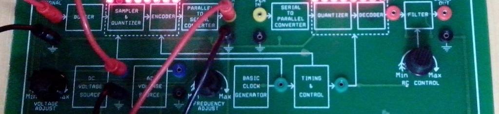
PAiA 4780 Twelve Stage Analog Sequencer Design Analysis Originally published 1974
 PAiA 4780 Twelve Stage Analog Sequencer Design Analysis Originally published 1974 DESIGN ANALYSIS: CLOCK As is shown in the block diagram of the sequencer (fig. 1) and the schematic (fig. 2), the clock
Exam Booklet. Pulse Circuits
 Exam Booklet Pulse Circuits Pulse Circuits STUDY ASSIGNMENT This booklet contains two examinations for the six lessons entitled Pulse Circuits. The material is intended to provide the last training sought
10-Bit µp-compatible D/A converter
 DESCRIPTION The is a microprocessor-compatible monolithic 10-bit digital-to-analog converter subsystem. This device offers 10-bit resolution and ±0.1% accuracy and monotonicity guaranteed over full operating
LINEAR IC APPLICATIONS
 1 B.Tech III Year I Semester (R09) Regular & Supplementary Examinations December/January 2013/14 1 (a) Why is R e in an emitter-coupled differential amplifier replaced by a constant current source? (b)
DEPARTMENT OF ELECTRICAL ENGINEERING LAB WORK EE301 ELECTRONIC CIRCUITS
 DEPARTMENT OF ELECTRICAL ENGINEERING LAB WORK EE301 ELECTRONIC CIRCUITS EXPERIMENT : 4 TITLE : 555 TIMERS OUTCOME : Upon completion of this unit, the student should be able to: 1. gain experience with
AD557 SPECIFICATIONS. T A = 25 C, V CC = 5 V unless otherwise noted) REV. B
 REV. B") SPECIFICATIONS Model Min Typ Max Unit RESOLUTION 8 Bits RELATIVE ACCURACY 0 C to 70 C ± 1/2 1 LSB Ranges 0 to 2.56 V Current Source 5 ma Sink Internal Passive Pull-Down to Ground 2 SETTLING TIME 3 0.8
SPECIFICATIONS Model Min Typ Max Unit RESOLUTION 8 Bits RELATIVE ACCURACY 0 C to 70 C ± 1/2 1 LSB Ranges 0 to 2.56 V Current Source 5 ma Sink Internal Passive Pull-Down to Ground 2 SETTLING TIME 3 0.8
ADC Bit A/D Converter
 ADC0800 8-Bit A/D Converter General Description The ADC0800 is an 8-bit monolithic A/D converter using P-channel ion-implanted MOS technology. It contains a high input impedance comparator, 256 series
1 Analog and Digital Communication Lab
 1 2 Amplitude modulator trainer kit diagram AM Detector trainer kit Diagram 3 4 Calculations: 5 Result: 6 7 8 Balanced modulator circuit diagram Generation of DSB-SC 1. For the same circuit apply the modulating
DACPORT Low Cost, Complete P-Compatible 8-Bit DAC AD557*
 a FEATURES Complete 8-Bit DAC Voltage Output 0 V to 2.56 V Internal Precision Band-Gap Reference Single-Supply Operation: 5 V ( 10%) Full Microprocessor Interface Fast: 1 s Voltage Settling to 1/2 LSB
Government Polytechnic Muzaffarpur Name of the Lab: Applied Electronics Lab
 Government Polytechnic Muzaffarpur Name of the Lab: Applied Electronics Lab Subject Code: 1620408 Experiment-1 Aim: To obtain the characteristics of field effect transistor (FET). Theory: The Field Effect
DEPARTMENT OF E.C.E.
 PVP SIDDHARTHA INSTITUTE OF TECHNOLOGY, KANURU, VIJAYAWADA-7 DEPARTMENT OF E.C.E. ANALOG COMMUNICATIONS LAB MANUAL Department of Electronics & Communication engineering Prasad V.Potluri Siddhartha Institute
OBSOLETE. 16-Bit/18-Bit, 16 F S PCM Audio DACs AD1851/AD1861
 a FEATURES 0 db SNR Fast Settling Permits 6 Oversampling V Output Optional Trim Allows Super-Linear Performance 5 V Operation 6-Pin Plastic DIP and SOIC Packages Pin-Compatible with AD856 & AD860 Audio
Amplitude modulator trainer kit diagram
 Amplitude modulator trainer kit diagram AM Detector trainer kit Diagram Calculations: Result: Pre lab test (20) Observation (20) Simulation (20) Remarks & Signature with Date Circuit connection (30) Result
Operating Manual Ver.1.1
 Multivibrators (Astable and Monostable) Operating Manual Ver.1.1 An ISO 9001 : 2000 company 94-101, Electronic Complex Pardesipura, Indore- 452010, India Tel : 91-731- 2570301/02, 4211100 Fax: 91-731-
8-Bit, high-speed, µp-compatible A/D converter with track/hold function ADC0820
 8-Bit, high-speed, µp-compatible A/D converter with DESCRIPTION By using a half-flash conversion technique, the 8-bit CMOS A/D offers a 1.5µs conversion time while dissipating a maximum 75mW of power.
1 Signals and systems, A. V. Oppenhaim, A. S. Willsky, Prentice Hall, 2 nd edition, FUNDAMENTALS. Electrical Engineering. 2.
 1 Signals and systems, A. V. Oppenhaim, A. S. Willsky, Prentice Hall, 2 nd edition, 1996. FUNDAMENTALS Electrical Engineering 2.Processing - Analog data An analog signal is a signal that varies continuously.
The steeper the phase shift as a function of frequency φ(ω) the more stable the frequency of oscillation
 the more stable the frequency of oscillation") It should be noted that the frequency of oscillation ω o is determined by the phase characteristics of the feedback loop. the loop oscillates at the frequency for which the phase is zero The steeper the
It should be noted that the frequency of oscillation ω o is determined by the phase characteristics of the feedback loop. the loop oscillates at the frequency for which the phase is zero The steeper the
Difference between BJTs and FETs. Junction Field Effect Transistors (JFET)
") Difference between BJTs and FETs Transistors can be categorized according to their structure, and two of the more commonly known transistor structures, are the BJT and FET. The comparison between BJTs
Difference between BJTs and FETs Transistors can be categorized according to their structure, and two of the more commonly known transistor structures, are the BJT and FET. The comparison between BJTs
CMOS Schmitt Trigger A Uniquely Versatile Design Component
 CMOS Schmitt Trigger A Uniquely Versatile Design Component INTRODUCTION The Schmitt trigger has found many applications in numerous circuits, both analog and digital. The versatility of a TTL Schmitt is
ML4818 Phase Modulation/Soft Switching Controller
 Phase Modulation/Soft Switching Controller www.fairchildsemi.com Features Full bridge phase modulation zero voltage switching circuit with programmable ZV transition times Constant frequency operation
INSTITUTE OF AERONAUTICAL ENGINEERING (Autonomous) Dundigal, Hyderabad
 Dundigal, Hyderabad") 1 P a g e INSTITUTE OF AERONAUTICAL ENGINEERING (Autonomous) Dundigal, Hyderabad - 500 043 ELECTRONICS AND COMMUNICATION ENGINEERING TUTORIAL QUESTION BANK Name : INTEGRATED CIRCUITS APPLICATIONS Code
1 P a g e INSTITUTE OF AERONAUTICAL ENGINEERING (Autonomous) Dundigal, Hyderabad - 500 043 ELECTRONICS AND COMMUNICATION ENGINEERING TUTORIAL QUESTION BANK Name : INTEGRATED CIRCUITS APPLICATIONS Code
CHAPTER 4: 555 TIMER. Dr. Wan Mahani Hafizah binti Wan Mahmud
 CHAPTE 4: 555 TIME Dr. Wan Mahani Hafizah binti Wan Mahmud 555 TIME Introduction Pin configuration Basic architecture and operation Astable Operation Monostable Operation Timer in Triggering Circuits 555
CONTENTS Sl. No. Experiment Page No
 CONTENTS Sl. No. Experiment Page No 1a Given a 4-variable logic expression, simplify it using Entered Variable Map and realize the simplified logic expression using 8:1 multiplexer IC. 2a 3a 4a 5a 6a 1b
Low Cost 10-Bit Monolithic D/A Converter AD561
 a FEATURES Complete Current Output Converter High Stability Buried Zener Reference Laser Trimmed to High Accuracy (1/4 LSB Max Error, AD561K, T) Trimmed Output Application Resistors for 0 V to +10 V, 5
Lab 7: DELTA AND SIGMA-DELTA A/D CONVERTERS
 ANALOG & TELECOMMUNICATION ELECTRONICS LABORATORY EXERCISE 6 Lab 7: DELTA AND SIGMA-DELTA A/D CONVERTERS Goal The goals of this experiment are: - Verify the operation of a differential ADC; - Find the
COMMUNICATIONS LAB. Duration of University Examination University Examination
 COMMUNICATIONS LAB Instructions Duration of University Examination University Examination Sessional 4 Periods per week 3 Hours 50 Marks 25 Marks Course Objectives: 1. Demonstrate AM, FM, Mixer, PAM, PWM
Tel: Fax:
 B Tel: 78.39.4700 Fax: 78.46.33 SPECIFICATIONS (T A = +5 C, V+ = +5 V, V = V or 5 V, all voltages measured with respect to digital common, unless otherwise noted) AD57J AD57K AD57S Model Min Typ Max Min
Dev Bhoomi Institute Of Technology Department of Electronics and Communication Engineering PRACTICAL INSTRUCTION SHEET REV. NO. : REV.
 Dev Bhoomi Institute Of Technology Department of Electronics and Communication Engineering PRACTICAL INSTRUCTION SHEET LABORATORY MANUAL EXPERIMENT NO. ISSUE NO. : ISSUE DATE: July 200 REV. NO. : REV.
the elektor datasheet collection
 the elektor datasheet collection LM117 LM136 LM137 L200 LM236 LM317 1,2...37 V/1,5 A Shunt regulator 2,5 V -1,2...-37 V/1,5 A 2,8...36 V/2 A Shunt regulator 2,5 V 1,2...37 V/1,5 A LM320LZ-12 Fixed voltage
Multivibrators. Department of Electrical & Electronics Engineering, Amrita School of Engineering
 Multivibrators Multivibrators Multivibrator is an electronic circuit that generates square, rectangular, pulse waveforms. Also called as nonlinear oscillators or function generators. Multivibrator is basically
1. LINEAR WAVE SHAPING
 Aim: 1. LINEAR WAVE SHAPING i) To design a low pass RC circuit for the given cutoff frequency and obtain its frequency response. ii) To observe the response of the designed low pass RC circuit for the
LM2240 Programmable Timer Counter
 LM2240 Programmable Timer Counter General Description The LM2240 Programmable Timer Counter is a monolithic controller capable of both monostable and astable operation Monostable operation allows accurate
Summer 2015 Examination
 Summer 2015 Examination Subject Code: 17445 Model Answer Important Instructions to examiners: 1) The answers should be examined by key words and not as word-to-word as given in the model answer scheme.
8-Bit A/D Converter AD673 REV. A FUNCTIONAL BLOCK DIAGRAM
 a FEATURES Complete 8-Bit A/D Converter with Reference, Clock and Comparator 30 s Maximum Conversion Time Full 8- or 16-Bit Microprocessor Bus Interface Unipolar and Bipolar Inputs No Missing Codes Over
6. HARDWARE PROTOTYPE AND EXPERIMENTAL RESULTS
 6. HARDWARE PROTOTYPE AND EXPERIMENTAL RESULTS Laboratory based hardware prototype is developed for the z-source inverter based conversion set up in line with control system designed, simulated and discussed
GOVERNMENT OF KARNATAKA KARNATAKA STATE PRE-UNIVERSITY EDUCATION EXAMINATION BOARD II YEAR PUC EXAMINATION MARCH-2013 SCHEME OF VALUATION
 GOVERNMENT OF KARNATAKA KARNATAKA STATE PRE-UNIVERSITY EDUCATION EXAMINATION BOARD II YEAR PUC EXAMINATION MARCH-03 SCHEME OF VALUATION Subject Code: 0 Subject: PART - A 0. What does the arrow mark indicate
UNIT-I CIRCUIT CONFIGURATION FOR LINEAR
 UNIT-I CIRCUIT CONFIGURATION FOR LINEAR ICs 2 marks questions 1.Mention the advantages of integrated circuits. *Miniaturisation and hence increased equipment density. *Cost reduction due to batch processing.
Concepts to be Reviewed
 Introductory Medical Device Prototyping Analog Circuits Part 3 Operational Amplifiers, http://saliterman.umn.edu/ Department of Biomedical Engineering, University of Minnesota Concepts to be Reviewed Operational
PESIT BANGALORE SOUTH CAMPUS BASIC ELECTRONICS
 PESIT BANGALORE SOUTH CAMPUS QUESTION BANK BASIC ELECTRONICS Sub Code: 17ELN15 / 17ELN25 IA Marks: 20 Hrs/ Week: 04 Exam Marks: 80 Total Hours: 50 Exam Hours: 03 Name of Faculty: Mr. Udoshi Basavaraj Module
Massachusetts Institute of Technology MIT
 Massachusetts Institute of Technology MIT Real Time Wireless Electrocardiogram (ECG) Monitoring System Introductory Analog Electronics Laboratory Guilherme K. Kolotelo, Rogers G. Reichert Cambridge, MA
Basic Operational Amplifier Circuits
 Basic Operational Amplifier Circuits Comparators A comparator is a specialized nonlinear op-amp circuit that compares two input voltages and produces an output state that indicates which one is greater.
Lab 2 Revisited Exercise
 Lab 2 Revisited Exercise +15V 100k 1K 2N2222 Wire up led display Note the ground leads LED orientation 6.091 IAP 2008 Lecture 3 1 Comparator, Oscillator +5 +15 1k 2 V- 7 6 Vin 3 V+ 4 V o Notice that power
Advanced Regulating Pulse Width Modulators
 Advanced Regulating Pulse Width Modulators FEATURES Complete PWM Power Control Circuitry Uncommitted Outputs for Single-ended or Push-pull Applications Low Standby Current 8mA Typical Interchangeable with
Microprocessor-Compatible 12-Bit D/A Converter AD667*
 a FEATURES Complete 12-Bit D/A Function Double-Buffered Latch On Chip Output Amplifier High Stability Buried Zener Reference Single Chip Construction Monotonicity Guaranteed Over Temperature Linearity
12-Bit Successive-Approximation Integrated Circuit A/D Converter AD ADC80
 a 2-Bit Successive-Approximation Integrated Circuit A/D Converter FEATURES True 2-Bit Operation: Max Nonlinearity.2% Low Gain T.C.: 3 ppm/ C Max Low Power: 8 mw Fast Conversion Time: 25 s Precision 6.3
multivibrator; Introduction to silicon-controlled rectifiers (SCRs).
.") Appendix The experiments of which details are given in this book are based largely on a set of 'modules' specially designed by Dr. K.J. Close. These 'modules' are now made and marketed by Irwin-Desman
Appendix The experiments of which details are given in this book are based largely on a set of 'modules' specially designed by Dr. K.J. Close. These 'modules' are now made and marketed by Irwin-Desman
For input: Peak to peak amplitude of the input = volts. Time period for 1 full cycle = sec
 Inverting amplifier: [Closed Loop Configuration] Design: A CL = V o /V in = - R f / R in ; Assume R in = ; Gain = ; Circuit Diagram: RF +10V F.G ~ + Rin 2 3 7 IC741 + 4 6 v0-10v CRO Model Graph Inverting
PHYS225 Lecture 18. Electronic Circuits
 PHYS225 Lecture 18 Electronic Circuits Oscillators and Timers Oscillators & Timers Produce timing signals to initiate measurement Periodic or single pulse Periodic output at known (controlled) frequency
GOVERNMENT OF KARNATAKA KARNATAKA STATE PRE-UNIVERSITY EDUCATION EXAMINATION BOARD II YEAR PUC EXAMINATION JULY-2012 SCHEME OF VALUATION
 GOVERNMENT OF KARNATAKA KARNATAKA STATE PRE-UNIVERSITY EDUCATION EXAMINATION BOARD II YEAR PUC EXAMINATION JULY-0 SCHEME OF VALUATION Subject Code: 40 Subject: PART - A 0. Which region of the transistor
DIGITAL ELECTRONICS ANALOG ELECTRONICS
 DIGITAL ELECTRONICS 1. N10 4 Bit Binary Universal shift register. 2. N22- Random Access Memory (16*4). 3. N23- Read Only Memory. 4. N4-R-S/D-T Flip flop, characteristic and comparison. 5. Master Slave
Operational Amplifiers
 Operational Amplifiers Table of contents 1. Design 1.1. The Differential Amplifier 1.2. Level Shifter 1.3. Power Amplifier 2. Characteristics 3. The Opamp without NFB 4. Linear Amplifiers 4.1. The Non-Inverting
Analog Electronic Circuits Lab-manual
 2014 Analog Electronic Circuits Lab-manual Prof. Dr Tahir Izhar University of Engineering & Technology LAHORE 1/09/2014 Contents Experiment-1:...4 Learning to use the multimeter for checking and indentifying
Speed Control of DC Motor Using Phase-Locked Loop
 Speed Control of DC Motor Using Phase-Locked Loop Authors Shaunak Vyas Darshit Shah Affiliations B.Tech. Electrical, Nirma University, Ahmedabad E-mail shaunak_vyas1@yahoo.co.in darshit_shah1@yahoo.co.in
P a g e 1. Introduction
 P a g e 1 Introduction 1. Signals in digital form are more convenient than analog form for processing and control operation. 2. Real world signals originated from temperature, pressure, flow rate, force
XR-8038A Precision Waveform Generator
 ...the analog plus company TM XR-0A Precision Waveform Generator FEATURES APPLICATIONS June 1- Low Frequency Drift, 50ppm/ C, Typical Simultaneous, Triangle, and Outputs Low Distortion - THD 1% High FM
LM231A/LM231/LM331A/LM331 Precision Voltage-to-Frequency Converters
 LM231A/LM231/LM331A/LM331 Precision Voltage-to-Frequency Converters General Description The LM231/LM331 family of voltage-to-frequency converters are ideally suited for use in simple low-cost circuits
Module -18 Flip flops
 1 Module -18 Flip flops 1. Introduction 2. Comparison of latches and flip flops. 3. Clock the trigger signal 4. Flip flops 4.1. Level triggered flip flops SR, D and JK flip flops 4.2. Edge triggered flip
Question Paper Code: 21398
 Reg. No. : Question Paper Code: 21398 B.E./B.Tech. DEGREE EXAMINATION, MAY/JUNE 2013 Fourth Semester Electrical and Electronics Engineering EE2254 LINEAR INTEGRATED CIRCUITS AND APPLICATIONS (Regulation
SEM: V EXAM MARKS: 50 BRANCH: EC IA MARKS: 25 SUBJECT: ANALOG COMMUNICATION & LIC LAB SUB CODE: 06ECL58
 LIST OF EXPERIMENTS SEM: V EXAM MARKS: 50 BRANCH: EC IA MARKS: 25 SUBJECT: ANALOG COMMUNICATION & LIC LAB SUB CODE: 06ECL58 1) Active low pass & high pass filters second order 2) Active band pass & band
EXPERIMENT 2.2 NON-LINEAR OP-AMP CIRCUITS
 2.16 EXPERIMENT 2.2 NONLINEAR OPAMP CIRCUITS 2.2.1 OBJECTIVE a. To study the operation of 741 opamp as comparator. b. To study the operation of active diode circuits (precisions circuits) using opamps,
OBJECTIVE The purpose of this exercise is to design and build a pulse generator.
 ELEC 4 Experiment 8 Pulse Generators OBJECTIVE The purpose of this exercise is to design and build a pulse generator. EQUIPMENT AND PARTS REQUIRED Protoboard LM555 Timer, AR resistors, rated 5%, /4 W,
A Simplified Test Set for Op Amp Characterization
 A Simplified Test Set for Op Amp Characterization INTRODUCTION The test set described in this paper allows complete quantitative characterization of all dc operational amplifier parameters quickly and
CHAPTER IV DESIGN AND ANALYSIS OF VARIOUS PWM TECHNIQUES FOR BUCK BOOST CONVERTER
 59 CHAPTER IV DESIGN AND ANALYSIS OF VARIOUS PWM TECHNIQUES FOR BUCK BOOST CONVERTER 4.1 Conventional Method A buck-boost converter circuit is a combination of the buck converter topology and a boost converter
DEPARTMENT OF ELECTRICAL & ELECTRONICS ENGINEERING
 DEPARTMENT OF ELECTRICAL & ELECTRONICS ENGINEERING (Regulation 2013) EE 6311 LINEAR AND DIGITAL INTEGRATED CIRCUITS LAB MANUAL 1 SYLLABUS OBJECTIVES: Working Practice in simulators / CAD Tools / Experiment
LM13600 Dual Operational Transconductance Amplifiers with Linearizing Diodes and Buffers
 LM13600 Dual Operational Transconductance Amplifiers with Linearizing Diodes and Buffers General Description The LM13600 series consists of two current controlled transconductance amplifiers each with
LABORATORY EXPERIMENT. Infrared Transmitter/Receiver
 LABORATORY EXPERIMENT Infrared Transmitter/Receiver (Note to Teaching Assistant: The week before this experiment is performed, place students into groups of two and assign each group a specific frequency
COMPARATOR CHARACTERISTICS The important characteristics of a comparator are these: 1. Speed of operation 2. Accuracy 3. Compatibility of output
 SCHMITT TRIGGER (regenerative comparator) Schmitt trigger is an inverting comparator with positive feedback. It converts an irregular-shaped waveform to a square wave or pulse, also called as squaring
OBJECTIVE TYPE QUESTIONS
 OBJECTIVE TYPE QUESTIONS Q.1 The breakdown mechanism in a lightly doped p-n junction under reverse biased condition is called (A) avalanche breakdown. (B) zener breakdown. (C) breakdown by tunnelling.
EE 3101 ELECTRONICS I LABORATORY EXPERIMENT 9 LAB MANUAL APPLICATIONS OF IC BUILDING BLOCKS
 EE 3101 ELECTRONICS I LABORATORY EXPERIMENT 9 LAB MANUAL APPLICATIONS OF IC BUILDING BLOCKS OBJECTIVES In this experiment you will Explore the use of a popular IC chip and its applications. Become more
ELECTRONICS ADVANCED SUPPLEMENTARY LEVEL
 ELECTRONICS ADVANCED SUPPLEMENTARY LEVEL AIMS The general aims of the subject are : 1. to foster an interest in and an enjoyment of electronics as a practical and intellectual discipline; 2. to develop
Chapter 2 Signal Conditioning, Propagation, and Conversion
 09/0 PHY 4330 Instrumentation I Chapter Signal Conditioning, Propagation, and Conversion. Amplification (Review of Op-amps) Reference: D. A. Bell, Operational Amplifiers Applications, Troubleshooting,
LM2900 LM3900 LM3301 Quad Amplifiers
 LM2900 LM3900 LM3301 Quad Amplifiers General Description The LM2900 series consists of four independent dual input internally compensated amplifiers which were designed specifically to operate off of a
NJM4151 V-F / F-V CONVERTOR
 V-F / F-V CONVERTOR GENERAL DESCRIPTION PACKAGE OUTLINE The NJM4151 provide a simple low-cost method of A/D conversion. They have all the inherent advantages of the voltage-to-frequency conversion technique.
Process Components. Process component
 What are PROCESS COMPONENTS? Input Transducer Process component Output Transducer The input transducer circuits are connected to PROCESS COMPONENTS. These components control the action of the OUTPUT components
Gechstudentszone.wordpress.com
 8.1 Operational Amplifier (Op-Amp) UNIT 8: Operational Amplifier An operational amplifier ("op-amp") is a DC-coupled high-gain electronic voltage amplifier with a differential input and, usually, a single-ended
GATE SOLVED PAPER - IN
 YEAR 202 ONE MARK Q. The i-v characteristics of the diode in the circuit given below are : v -. A v 0.7 V i 500 07 $ = * 0 A, v < 0.7 V The current in the circuit is (A) 0 ma (C) 6.67 ma (B) 9.3 ma (D)
Phase-locked loop PIN CONFIGURATIONS
 NE/SE DESCRIPTION The NE/SE is a versatile, high guaranteed frequency phase-locked loop designed for operation up to 0MHz. As shown in the Block Diagram, the NE/SE consists of a VCO, limiter, phase comparator,
Applications of the LM392 Comparator Op Amp IC
 Applications of the LM392 Comparator Op Amp IC The LM339 quad comparator and the LM324 op amp are among the most widely used linear ICs today. The combination of low cost, single or dual supply operation
EG572EX: ELECTRONIC CIRCUITS I 555 TIMERS
 EG572EX: ELECTRONIC CIRCUITS I 555 TIMERS Prepared By: Ajay Kumar Kadel, Kathmandu Engineering College 1) PIN DESCRIPTIONS Fig.1 555 timer Pin Configurations Pin 1 (Ground):- All voltages are measured
16-Bit ANALOG-TO-DIGITAL CONVERTER
 16-Bit ANALOG-TO-DIGITAL CONVERTER FEATURES 16-BIT RESOLUTION LINEARITY ERROR: ±0.003% max (KG, BG) NO MISSING CODES GUARANTEED FROM 25 C TO 85 C 17µs CONVERSION TIME (16-Bit) SERIAL AND PARALLEL OUTPUTS
FSK DEMODULATOR / TONE DECODER
 FSK DEMODULATOR / TONE DECODER GENERAL DESCRIPTION The is a monolithic phase-locked loop (PLL) system especially designed for data communications. It is particularly well suited for FSK modem applications,
 SET - 1 1. a) Write the application of attenuator b) State the clamping theorem c) Write the application of Monostable multi vibrator d) Draw the diagram for Diode two input AND gate e) Define the terms
ADC Bit µp Compatible A/D Converter
 ADC1001 10-Bit µp Compatible A/D Converter General Description The ADC1001 is a CMOS, 10-bit successive approximation A/D converter. The 20-pin ADC1001 is pin compatible with the ADC0801 8-bit A/D family.
A 7ns, 6mA, Single-Supply Comparator Fabricated on Linear s 6GHz Complementary Bipolar Process
 A 7ns, 6mA, Single-Supply Comparator Fabricated on Linear s 6GHz Complementary Bipolar Process Introduction The is an ultrafast (7ns), low power (6mA), single-supply comparator designed to operate on either
ANALOG TO DIGITAL CONVERTER
 Final Project ANALOG TO DIGITAL CONVERTER As preparation for the laboratory, examine the final circuit diagram at the end of these notes and write a brief plan for the project, including a list of the