Introduction to Full-Custom Circuit Design with HSPICE and Laker
|
|
|
- Kerry Grant
- 5 years ago
- Views:
Transcription

1 Introduction to VLSI and SOC Design Introduction to Full-Custom Circuit Design with HSPICE and Laker Course Instructor: Prof. Lan-Da Van T.A.: Tsung-Che Lu Department of Computer Science National Chiao Tung University Taiwan, R.O.C. Fall, 2009

2 Environment Setup Tool Pietty Xming
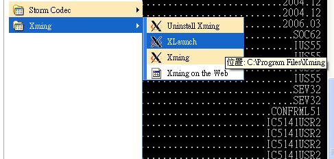
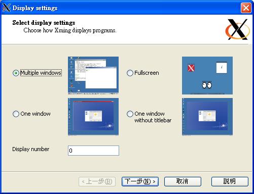
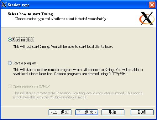
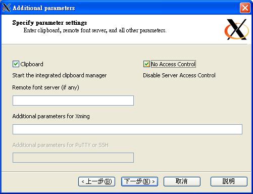
3 Environment Setup (Xming) Open Xming No Access Control

4 Environment Setup (Pietty) Server: hwlab01.cs.nctu.edu.tw ~ hwlab08.cs.nctu.edu.tw Password could be changed on hwlab01 only. Your IP:0
5 Simulation with HSPICE Introduction to VLSI and SOC Design
6 Annotation (with * start) Part 1 Part 2 A Typical SPICE Script * cmos inverter.include mosistsmc180.sp Model File * sub circuit component netlist.subckt inv in out gnd vdd ma out in gnd gnd NMOS L=0.18u W=0.36u mb out in vdd vdd PMOS L=0.18u W=0.72u.ends Transistor Type * voltage source X1 in out gnd vdd inv v1 vdd 0 1.8V v2 gnd 0 0V v3 in 0 pulse ( ns 0.01ns 0.01ns 0.5ns 1ns) in VDD GND out Part 3 * simulation environment.option post.tran 0.05ns 3ns Specification Measurement.meas tran td1 trig v(in) val=0.9 rise=1 targ v(out) val=0.9 fall=1.meas tran td2 trig v(in) val=0.9 fall=1 targ v(out) val=0.9 rise=1.end End of the script
7 Basic Syntax in HSPICE (1/2) MOS Transistor: ma out in gnd gnd NMOS L=0.18u W=0.36u Mx (drain) (gate) (source) (body) (Type of MOST) + L=(length) W=(width) Capacitor: C p : There s a 5pF capacitor C1 between node 1 & node 0 Resistor: R k : There s a 5k(ohm) resistor R1 between node 2 & node 0 DC Voltage Source V1 VDD 0 1.8V : There s a 1.8V voltage source V1 between node VDD & node 0 Notice: Node 0 is considered as GROUND in SPICE simulation. Never use a node name with numbers in the front part. (Ex: 2P, 3A)
8 Basic Syntax in HSPICE (2/2) Subcircuit Syntax:.subckt inv in out gnd vdd ma out in gnd gnd NMOS L=0.18u W=0.36u mb out in vdd vdd PMOS L=0.18u W=0.72u.ends This is a sub-circuit called inv which has 4 nodes called in, out, gnd and vdd Subcircuit Calls: X1 in out gnd vdd inv A subcircuit X1 is called by netlist and its type is inv
9 Analysis Type Transient Analysis:.tran 0.05ns 3ns Above syntax will ask SPICE to simulate the circuit s waveform from 0ns to 3ns with a interval of 0.05ns. DC Analysis:.dc vds Above syntax will ask SPICE to simulate the circuit s DC operating point as the variable vds changing from 0 to 1.8 with a interval of 0.05.

10 Pulse Source Function Figure Source: 王朝琴, SPICE Training Manual, CIC, July, 2005

11 Piecewise Linear Function Figure Source: 王朝琴, SPICE Training Manual, CIC, July, 2005

12 MEASURE: Application Examples Figure Source: 王朝琴, SPICE Training Manual, CIC, July, 2005

13 Run HSPICE Job Concluded Command: hspice i xxx.sp -o xxx.lis If Job Aborted, see xxx.lis file for detailed imformation. The measured specifications and power consumption will be listed in.lis file. The simulated waveform will be saved in.tr0 file.
14 .meas Output Format in.lis file ****** transient analysis tnom= temp= ****** td1= E-12 targ= E-10 trig= E-10 td2= E-11 targ= E-10 trig= E-10 ***** job concluded
")

15 Waveform Viewer - nwave (1/3) File Open Command: nwave &.tr0 *.*
")

16 Waveform Viewer - nwave (2/3) Get Signals Choose input & output node
 Press 100% button")
17 Waveform Viewer - nwave (3/3) Press 100% button
18 Layout with Laker Introduction to VLSI and SOC Design

19 CMOS Cross-section Figure Source: F. Maloberti, Analog Design for CMOS VLSI Systems N. H. E Weste and D. Harris, CMOS

20 NMOS Contact Poly Diffusion Width (W) Length (L) NIMP PIMP Metal1 Figure Source:

21 PMOS Contact Metal1 NIMP PIMP Diffusion NWell Poly Figure Source:
 Library New Create a new")
22 Laker - Create a New Library (1/1) Library New Create a new library

23 Laker - Create a New Library (2/2) Enter library name /cad/cbdlib/cic18/laker/laker.tf


24 Laker - Create a New Cell Cell New


25 Laker Change Grid Change Gird 0.01
26 Laker - Hotkeys r: rectangle u: undo k: ruler Shift + k: remove rulers Delete: delete shapes or lines Esc: back to cmd(selecting) Shift + p: polygon Ctrl + z: zoom in Shift + z: zoom out f: fit design c: copy m: move p: path l: text cmd(selecting) + ctrl + a: select all
27 Inverter (1/3) Schematic Stick Diagram VDD P-diff Vin N-diff Vout GND Figure Source:

28 Inverter (2/3) Figure Source:

29 Inverter (3/3) Figure Source:


30 0.18um 1P6M Process Layers Diffusion N-Well P Implant N Implant CONT Poly Metal 1 VIA
31 Verification and Extraction with Calibre DRC (Design Rule Check) Check for design rule violations LVS (Layout versus Schematic Check) Check for inconsistencies between the physical layout and the schematic PEX (Parasitic Extraction) / LPE (Layout Parameter Extraction) Extract layout parameters, such as transistors, parasitic capacitor, and parasitic resistors Extracted netlist

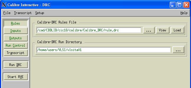
32 DRC with Calibre (1/3) Verify Calibre Run DRC /cad/cbdlib/cic18/calibre/calibre_drc/rule.drc
 Must be")
33 DRC with Calibre (2/3) Must be selected!


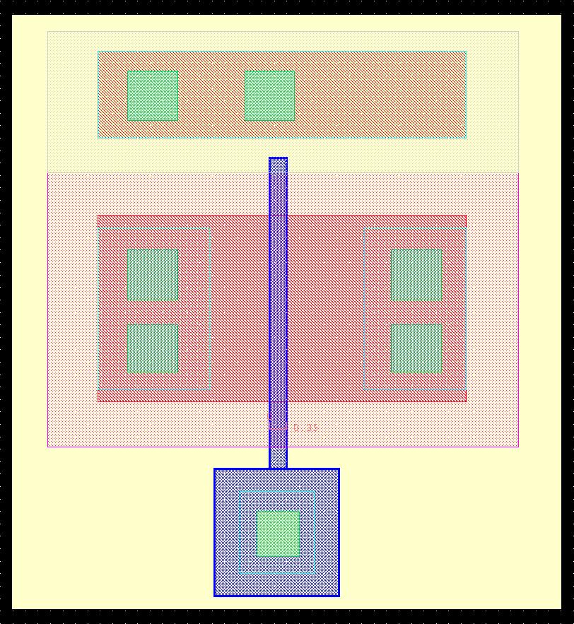
34 DRC with Calibre (3/3) Total Errors Count Clear Highlight The errors of DRC must be modified for error free! Double Click Detailed Information about errors Highlight on your layout
35 Lab Requirement Copy is strictly prohibited, and doing the assigned labs on your own is required. Otherwise, you will get zero score for no excuse. Please notice the lately delivered reports will not be accepted after due date. Detailed information and report format will be announced on the course forum/website. The designate model file (mosistsmc180.sp) can be downloaded from SPICE and Verilog code link in textbook s website. The course forum is available now. Any question/ discussion can be posted on board or TAs.
Introduction to VLSI design using Cadence Electronic Design Automation Tools
 Bangladesh University of Engineering & Technology Department of Electrical & Electronic Engineering Introduction to VLSI design using Cadence Electronic Design Automation Tools Laboratory Module 4: Layout
HSPICE. Chan-Ming Chang
 HSPICE Chan-Ming Chang Outline Declaration Voltage source Circuit statement SUBCKT of circuit statement Measure Simulation Declaration ***** SPICE COURSE EXAMPLE INVERTER LJC *****.LIB 'mm018.l' tt.global
Elad Alon HW #1: Circuit Simulation EECS 141 Due Thursday, Aug. 30th, 5pm, box in 240 Cory
 UNIVERSITY OF CALIFORNIA College of Engineering Department of Electrical Engineering and Computer Sciences Last modified on August 20, 2012 by Elad Alon Elad Alon HW #1: Circuit Simulation EECS 141 Due
SPICE Simulation Program with Integrated Circuit Emphasis
 SPICE Simulation Program with Integrated Circuit Emphasis References: [1] CIC SPICE training manual [3] SPICE manual [2] DIC textbook Sep. 25, 2004 1 SPICE: Introduction Simulation Program with Integrated
Intelligent Systems Group Department of Electronics. An Evolvable, Field-Programmable Full Custom Analogue Transistor Array (FPTA)
") Department of Electronics n Evolvable, Field-Programmable Full Custom nalogue Transistor rray (FPT) Outline What`s Behind nalog? Evolution Substrate custom made configurable transistor array (FPT) Ways
Department of Electronics n Evolvable, Field-Programmable Full Custom nalogue Transistor rray (FPT) Outline What`s Behind nalog? Evolution Substrate custom made configurable transistor array (FPT) Ways
The default account setup for the class should allow you to run HSPICE without any further configuration. To verify this, type:
 UNIVERSITY OF CALIFORNIA College of Engineering Department of Electrical Engineering and Computer Sciences HW #1: Circuit Simulation NTU IC541CA (Spring 2004) 1 Objective The objective of this homework
Lecture 7: SPICE Simulation
 Lecture 7: SPICE Simulation Slides courtesy of Deming Chen Slides based on the initial set from David Harris CMOS VLSI Design Outline Introduction to SPICE DC Analysis Transient Analysis Subcircuits Optimization
ECEN 474/704 Lab 1: Introduction to Cadence & MOS Device Characterization
 ECEN 474/704 Lab 1: Introduction to Cadence & MOS Device Characterization Objectives Learn how to login on a Linux workstation, perform basic Linux tasks, and use the Cadence design system to simulate
EEC 116 Fall 2011 Lab #2: Analog Simulation Tutorial
 EEC 116 Fall 2011 Lab #2: Analog Simulation Tutorial Dept. of Electrical and Computer Engineering University of California, Davis Issued: September 28, 2011 Due: October 12, 2011, 4PM Reading: Rabaey Chapters
! Review: MOS IV Curves and Switch Model. ! MOS Device Layout. ! Inverter Layout. ! Gate Layout and Stick Diagrams. ! Design Rules. !
 ESE 570: Digital Integrated Circuits and VLSI Fundamentals Lec 3: January 21, 2017 MOS Fabrication pt. 2: Design Rules and Layout Lecture Outline! Review: MOS IV Curves and Switch Model! MOS Device Layout!
Sticks Diagram & Layout. Part II
 Sticks Diagram & Layout Part II Well and Substrate Taps Substrate must be tied to GND and n-well to V DD Metal to lightly-doped semiconductor forms poor connection called Shottky Diode Use heavily doped
Mentor Analog Simulators
 ENGR-434 Spice Netlist Syntax Details Introduction Rev 5/25/11 As you may know, circuit simulators come in several types. They can be broadly grouped into those that simulate a circuit in an analog way,
! Review: MOS IV Curves and Switch Model. ! MOS Device Layout. ! Inverter Layout. ! Gate Layout and Stick Diagrams. ! Design Rules. !
 ESE 570: Digital Integrated Circuits and VLSI Fundamentals Lec 3: January 21, 2016 MOS Fabrication pt. 2: Design Rules and Layout Lecture Outline! Review: MOS IV Curves and Switch Model! MOS Device Layout!
ESE 570: Digital Integrated Circuits and VLSI Fundamentals
 ESE 570: Digital Integrated Circuits and VLSI Fundamentals Lec 3: January 21, 2016 MOS Fabrication pt. 2: Design Rules and Layout Penn ESE 570 Spring 2016 Khanna Adapted from GATech ESE3060 Slides Lecture
Figure 1. Main window (Common Interface Window), CIW opens and from the pull down menus you can start your design. Figure 2.
, CIW opens and from the pull down menus you can start your design. Figure 2.") Running Cadence Once the Cadence environment has been setup you can start working with Cadence. You can run cadence from your directory by typing Figure 1. Main window (Common Interface Window), CIW opens
Running Cadence Once the Cadence environment has been setup you can start working with Cadence. You can run cadence from your directory by typing Figure 1. Main window (Common Interface Window), CIW opens
Jack Keil Wolf Lecture. ESE 570: Digital Integrated Circuits and VLSI Fundamentals. Lecture Outline. MOSFET N-Type, P-Type.
 ESE 570: Digital Integrated Circuits and VLSI Fundamentals Jack Keil Wolf Lecture Lec 3: January 24, 2019 MOS Fabrication pt. 2: Design Rules and Layout http://www.ese.upenn.edu/about-ese/events/wolf.php
Introduction to Virtuoso & Calibre
 Introduction to Virtuoso & Calibre Courtesy of Dr. Harris @HMC, and Dr. Choi @PSU http://csce.uark.edu +1 (479) 575-6043 yrpeng@uark.edu Process Design Kit (PDK) The manufacturing grid defines the minimum
IC Layout Design of 4-bit Universal Shift Register using Electric VLSI Design System
 IC Layout Design of 4-bit Universal Shift Register using Electric VLSI Design System 1 Raj Kumar Mistri, 2 Rahul Ranjan, 1,2 Assistant Professor, RTC Institute of Technology, Anandi, Ranchi, Jharkhand,
EECE 488: Short HSPICE Tutorial. Last updated by: Mohammad Beikahmadi January 2013
 EECE 488: Short HSPICE Tutorial Last updated by: Mohammad Beikahmadi January 2013 SPICE? Simulation Program with Integrated Circuit Emphasis An open source analog circuit simulator Predicts circuit behavior,
ESE 570: Digital Integrated Circuits and VLSI Fundamentals
 ESE 570: Digital Integrated Circuits and VLSI Fundamentals Lec 3: January 24, 2019 MOS Fabrication pt. 2: Design Rules and Layout Penn ESE 570 Spring 2019 Khanna Jack Keil Wolf Lecture http://www.ese.upenn.edu/about-ese/events/wolf.php
Schematic and Layout Simulation Exercise
 University of California, Berkeley EE141 Fall 2009 Laboratory Exercise 4 Schematic and Layout Simulation Exercise The objective of this laboratory exercise is to walk you through the process of simulating
Lab 2: Basic Boolean Circuits. Brittany Duffy EE 330- Integrated Electronics Lab Section B Professor Randy Geiger 1/31/13
 Lab 2: Basic Boolean Circuits Brittany Duffy EE 330- Integrated Electronics Lab Section B Professor Randy Geiger 1/31/13 Introduction The main goal of this lab was to become familiarized with the methods
CMOS VLSI IC Design. A decent understanding of all tasks required to design and fabricate a chip takes years of experience
 CMOS VLSI IC Design A decent understanding of all tasks required to design and fabricate a chip takes years of experience 1 Commonly used keywords INTEGRATED CIRCUIT (IC) many transistors on one chip VERY
DIGITAL VLSI LAB ASSIGNMENT 1
 DIGITAL VLSI LAB ASSIGNMENT 1 Problem 1: NMOS and PMOS plots using Cadence. In this exercise, you are required to generate both NMOS and PMOS I-V device characteristics (I/P and O/P) using Cadence (Use
EECS 312: Digital Integrated Circuits Lab Project 1 Introduction to Schematic Capture and Analog Circuit Simulation
 EECS 312: Digital Integrated Circuits Lab Project 1 Introduction to Schematic Capture and Analog Circuit Simulation Teacher: Robert Dick GSI: Shengshuo Lu Assigned: 5 September 2013 Due: 17 September 2013
ETI063 - Analogue IC Design Laboratory Manual
 Department of Electrical and Information Technology ETI063 - Analogue IC Design Laboratory Manual Ellie Cijvat September 2009 CONTENTS i Contents Introduction 1 Laboratory Overview........................
Introduction to LT Spice IV with Examples
 Introduction to LT Spice IV with Examples 400D - Fall 2015 Purpose Part of Electronics & Control Division Technical Training Series by Nicholas Lombardo The purpose of this document is to give a basic
UNIVERSITY OF CALIFORNIA College of Engineering Department of Electrical Engineering and Computer Sciences
 UNIVERSITY OF CALIFORNIA College of Engineering Department of Electrical Engineering and Computer Sciences Jan M. Rabaey Homework #1: Circuit Simulation EECS 141 Due Friday, January 29, 5pm, box in 240
EECE 488: Short HSPICE. Tutorial. Last updated by: Mohammad Beikahmadi January Original presentation by: Jack Shiah
 EECE 488: Short HSPICE Tutorial Last updated by: Mohammad Beikahmadi January 2012 Original presentation by: Jack Shiah SPICE? Simulation Program with Integrated Circuit Emphasis An open source analog circuit
EE 330 Lecture 7. Design Rules
 EE 330 Lecture 7 Design Rules Last time: Response time of logic gates A Y C L t R C HL SWn L t R C LH SWp L C L proportional to #gates driven to avg input cap of gates R SW proportional length/width Last
! MOS Device Layout. ! Inverter Layout. ! Gate Layout and Stick Diagrams. ! Design Rules. ! Standard Cells. ! CMOS Process Enhancements
 EE 570: igital Integrated Circuits and VLI Fundamentals Lec 3: January 18, 2018 MO Fabrication pt. 2: esign Rules and Layout Lecture Outline! MO evice Layout! Inverter Layout! Gate Layout and tick iagrams!
Lab 3: Circuit Simulation with PSPICE
 Page 1 of 11 Laboratory Goals Introduce text-based PSPICE as a design tool Create transistor circuits using PSPICE Simulate output response for the designed circuits Introduce the Curve Tracer functionality.
Engineering 3821 Fall Pspice TUTORIAL 1. Prepared by: J. Tobin (Class of 2005) B. Jeyasurya E. Gill
 B. Jeyasurya E. Gill") Engineering 3821 Fall 2003 Pspice TUTORIAL 1 Prepared by: J. Tobin (Class of 2005) B. Jeyasurya E. Gill 2 INTRODUCTION The PSpice program is a member of the SPICE (Simulation Program with Integrated Circuit
Engineering 3821 Fall 2003 Pspice TUTORIAL 1 Prepared by: J. Tobin (Class of 2005) B. Jeyasurya E. Gill 2 INTRODUCTION The PSpice program is a member of the SPICE (Simulation Program with Integrated Circuit
EDA-BASED DESIGN PRACTICAL LABORATORY SESSION No. 4
 LABORATOIRE DE SYSTEMES MICROELECTRONIQUES EPFL STI IMM LSM ELD Station nº 11 CH-1015 Lausanne Téléphone : Fax : E-mail : Site web : +4121 693 6955 +4121 693 6959 lsm@epfl.ch lsm.epfl.ch EDA-BASED DESIGN
High-Speed Serial Interface Circuits and Systems
 High-Speed Serial Interface Circuits and Systems Design Exercise4 Charge Pump Charge Pump PLL ɸ ref up PFD CP LF VCO down ɸ out ɸ div Divider Converts PFD phase error pulse (digital) to charge (analog).
ESD-Transient Detection Circuit with Equivalent Capacitance-Coupling Detection Mechanism and High Efficiency of Layout Area in a 65nm CMOS Technology
 ESD-Transient Detection Circuit with Equivalent Capacitance-Coupling Detection Mechanism and High Efficiency of Layout Area in a 65nm CMOS Technology Chih-Ting Yeh (1, 2) and Ming-Dou Ker (1, 3) (1) Department
Conduction Characteristics of MOS Transistors (for fixed Vds)! Topic 2. Basic MOS theory & SPICE simulation. MOS Transistor
! Topic 2. Basic MOS theory & SPICE simulation. MOS Transistor") Conduction Characteristics of MOS Transistors (for fixed Vds)! Topic 2 Basic MOS theory & SPICE simulation Peter Cheung Department of Electrical & Electronic Engineering Imperial College London (Weste&Harris,
Conduction Characteristics of MOS Transistors (for fixed Vds)! Topic 2 Basic MOS theory & SPICE simulation Peter Cheung Department of Electrical & Electronic Engineering Imperial College London (Weste&Harris,
Topic 2. Basic MOS theory & SPICE simulation
 Topic 2 Basic MOS theory & SPICE simulation Peter Cheung Department of Electrical & Electronic Engineering Imperial College London (Weste&Harris, Ch 2 & 5.1-5.3 Rabaey, Ch 3) URL: www.ee.ic.ac.uk/pcheung/
Conduction Characteristics of MOS Transistors (for fixed Vds) Topic 2. Basic MOS theory & SPICE simulation. MOS Transistor
 Topic 2. Basic MOS theory & SPICE simulation. MOS Transistor") Conduction Characteristics of MOS Transistors (for fixed Vds) Topic 2 Basic MOS theory & SPICE simulation Peter Cheung Department of Electrical & Electronic Engineering Imperial College London (Weste&Harris,
Conduction Characteristics of MOS Transistors (for fixed Vds) Topic 2 Basic MOS theory & SPICE simulation Peter Cheung Department of Electrical & Electronic Engineering Imperial College London (Weste&Harris,
MOSFET: Mxxx nd ng ns nb modelname W=value L=value Ad As Pd Ps
 ELE447 Lab 1: Introduction to HSPICE In this lab, you will learn how to use HSPICE for simulating the electronic circuits. To be able to simulate a circuit using HSPICE, we need to write a text file that
Project #2 for Electronic Circuit II
 Project #2 for Electronic Circuit II Prof. Woo-Young Choi TA: Hyunkyu Kim, Minkyu Kim June 7, 2017 - Deadline : 6:00 pm on June 23, 2017. Penalties for late hand-in. - Team Students are expected to form
NGSPICE- Usage and Examples
 NGSPICE- Usage and Examples Debapratim Ghosh deba21pratim@gmail.com Electronic Systems Group Department of Electrical Engineering Indian Institute of Technology Bombay February 2013 Debapratim Ghosh Dept.
[Vivekanand*, 4.(12): December, 2015] ISSN: (I2OR), Publication Impact Factor: 3.785
![[Vivekanand*, 4.(12): December, 2015] ISSN: (I2OR), Publication Impact Factor: 3.785](/thumbs/84/90801833.jpg "[Vivekanand*, 4.(12): December, 2015] ISSN: (I2OR), Publication Impact Factor: 3.785") IJESRT INTERNATIONAL JOURNAL OF ENGINEERING SCIENCES & RESEARCH TECHNOLOGY DESIGN AND IMPLEMENTATION OF HIGH RELIABLE 6T SRAM CELL V.Vivekanand*, P.Aditya, P.Pavan Kumar * Electronics and Communication
IJESRT INTERNATIONAL JOURNAL OF ENGINEERING SCIENCES & RESEARCH TECHNOLOGY DESIGN AND IMPLEMENTATION OF HIGH RELIABLE 6T SRAM CELL V.Vivekanand*, P.Aditya, P.Pavan Kumar * Electronics and Communication
Design Rules, Technology File, DRC / LVS
 Design Rules, Technology File, DRC / LVS Prof. Dr. Peter Fischer VLSI Design: Design Rules P. Fischer, TI, Uni Mannheim, Seite 1 DESIGN RULES Rules in one Layer Caused by manufacturing limits (lithography,
Lecture Outline. ESE 570: Digital Integrated Circuits and VLSI Fundamentals. Previously: Two XOR Gates. Pass Transistor Logic. Cascaded Pass Gates
 ESE 570: Digital Integrated Circuits and VLSI Fundamentals Lecture Outline! Pass Transistor Logic! Performance Lec 15: March 2, 2017 Combination Logic: Pass Transistor Logic, and Performance 2 Previously:
Zero Steady State Current Power-on-Reset Circuit with Brown-Out Detector
 Zero Steady State Current Power-on-Reset Circuit with Brown-Out Detector Sanjay Kumar Wadhwa 1, G.K. Siddhartha 2, Anand Gaurav 3 Freescale Semiconductor India Pvt. Ltd. 1 sanjay.wadhwa@freescale.com,
Microelectronics, BSc course
 Microelectronics, BSc course MOS circuits: CMOS circuits, construction http://www.eet.bme.hu/~poppe/miel/en/14-cmos.pptx http://www.eet.bme.hu The abstraction level of our study: SYSTEM + MODULE GATE CIRCUIT
Project #3 for Electronic Circuit II
 Project #3 for Electronic Circuit II Prof. Woo-Young Choi TA: Tongsung Kim, Minkyu Kim June 1, 2015 - Deadline : 6:00 pm on June 22, 2015. Penalties for late hand-in. - Team Students are expected to form
Yuan-Piao Lee Te-Hsiu Chen Chienkuo Technology University, ChungHua, Taiwan, ROC
 Select the MODEL set HSPICE simulation results Yuan-Piao Lee Te-Hsiu Chen Chienkuo Technology University, ChungHua, Taiwan, ROC ABSTRACT To the the HSPICE design of circuit is quite convenient, this paper
Submission date: Wednesday 21/3/2018
 Faculty of Information Engineering & Technology Electrical & Electronics Department Course: Microelectronics Lab ELCT605 Spring 2018 Dr. Eman Azab Eng. Samar Shukry Analog Report 1, 2 DC, TRANSIENT, AND
Hot Topics and Cool Ideas in Scaled CMOS Analog Design
 Engineering Insights 2006 Hot Topics and Cool Ideas in Scaled CMOS Analog Design C. Patrick Yue ECE, UCSB October 27, 2006 Slide 1 Our Research Focus High-speed analog and RF circuits Device modeling,
EE 434 ASIC and Digital Systems. Prof. Dae Hyun Kim School of Electrical Engineering and Computer Science Washington State University.
 EE 434 ASIC and Digital Systems Prof. Dae Hyun Kim School of Electrical Engineering and Computer Science Washington State University Preliminaries VLSI Design System Specification Functional Design RTL
EEC 210 Fall 2008 Design Project. Rajeevan Amirtharajah Dept. of Electrical and Computer Engineering University of California, Davis
 EEC 210 Fall 2008 Design Project Rajeevan Amirtharajah Dept. of Electrical and Computer Engineering University of California, Davis Issued: November 18, 2008 Due: December 5, 2008, 5:00 PM in my office.
Chapter 1. Introduction
 EECS3611 Analog Integrated Circuit esign Chapter 1 Introduction EECS3611 Analog Integrated Circuit esign Instructor: Prof. Ebrahim Ghafar-Zadeh, Prof. Peter Lian email: egz@cse.yorku.ca peterlian@cse.yorku.ca
ECEN474/704: (Analog) VLSI Circuit Design Fall 2016
 VLSI Circuit Design Fall 2016") ECEN474/704: (Analog) VLSI Circuit Design Fall 2016 Lecture 1: Introduction Sam Palermo Analog & Mixed-Signal Center Texas A&M University Announcements Turn in your 0.18um NDA form by Thursday Sep 1 No
ECEN474/704: (Analog) VLSI Circuit Design Fall 2016 Lecture 1: Introduction Sam Palermo Analog & Mixed-Signal Center Texas A&M University Announcements Turn in your 0.18um NDA form by Thursday Sep 1 No
30 ma flash LDO voltage regulator (output voltage 1.8 ± 0.2 V)
") SPECIFICATION 1 FEATURES Global Foundries CMOS 55 nm Low drop out Low current consumption Two modes operations: Normal, Economy Mode operation Bypass No discrete filtering capacitors required (cap-less
SPECIFICATION 1 FEATURES Global Foundries CMOS 55 nm Low drop out Low current consumption Two modes operations: Normal, Economy Mode operation Bypass No discrete filtering capacitors required (cap-less
ECE 683 Project Report. Winter Professor Steven Bibyk. Team Members. Saniya Bhome. Mayank Katyal. Daniel King. Gavin Lim.
 ECE 683 Project Report Winter 2006 Professor Steven Bibyk Team Members Saniya Bhome Mayank Katyal Daniel King Gavin Lim Abstract This report describes the use of Cadence software to simulate logic circuits
Faculty of Engineering 4 th Year, Fall 2010
 4. Inverter Schematic a) After you open the previously created Inverter schematic, an empty window appears where you should place your components. To place an NMOS, select Add- >Instance or use shortcut
MHz phase-locked loop
 SPECIFICATION 1 FEATURES 50 800 MHz phase-locked loop TSMC CMOS 65 nm Output frequency from 50 to 800 MHz Reference frequency from 4 to 30 MHz Power supply 1.2 V CMOS output Supported foundries: TSMC,
CPE/EE 427, CPE 527 VLSI Design I: Homeworks 3 & 4
 CPE/EE 427, CPE 527 VLSI Design I: Homeworks 3 & 4 1 2 3 4 5 6 7 8 9 10 Sum 30 10 25 10 30 40 10 15 15 15 200 1. (30 points) Misc, Short questions (a) (2 points) Postponing the introduction of signals
ECEN 474/704 Lab 8: Two-Stage Miller Operational Amplifier
 ECEN 474/704 Lab 8: Two-Stage Miller Operational Amplifier Objective Design, simulate and test a two-stage operational amplifier Introduction Operational amplifiers (opamp) are essential components of
Layout - Line of Diffusion. Where are we? Line of Diffusion in General. Line of Diffusion in General. Stick Diagrams. Line of Diffusion in General
 Where are we? Lots of Layout issues Line of diffusion style Power pitch it-slice pitch Routing strategies Transistor sizing Wire sizing Layout - Line of Diffusion Very common layout method Start with a
Lecture Outline. ESE 570: Digital Integrated Circuits and VLSI Fundamentals. Teaser. Pass Transistor Logic. Identify Function.
 ESE 570: Digital Integrated Circuits and VLSI Fundamentals Lecture Outline! Pass Transistor Logic! Performance Lec 15: March 1, 2018 Combination Logic: Pass Transistor Logic, and Performance 2 Pass Transistor
EE 221 L CIRCUIT II. Learn to use LTspice to run circuit simulations for voltage, current, etc.
 EE 221 L CIRCUIT II LABORATORY 3: LTSPICE DEPARTMENT OF ELECTRICAL AND COMPUTER ENGINEERING UNIVERSITY OF NEVADA, LAS VEGAS OBJECTIVE Learn to use LTspice to run circuit simulations for voltage, current,
ECE520 VLSI Design. Lecture 5: Basic CMOS Inverter. Payman Zarkesh-Ha
 ECE520 VLSI Design Lecture 5: Basic CMOS Inverter Payman Zarkesh-Ha Office: ECE Bldg. 230B Office hours: Wednesday 2:00-3:00PM or by appointment E-mail: pzarkesh@unm.edu Slide: 1 Review of Last Lecture
Tsung-Chu Huang. Department of Electronic Engineering National Changhua University of Education /10/4-5 TCH NCUE
 Digital IC Design Tsung-Chu Huang Department of Electronic Engineering National Changhua University of Education Email: tch@cc.ncue.edu.tw 2004/10/4-5 Page 1 Circuit Simulation Tools 1. Switch Level: Verilog,
CHAPTER 6 DIGITAL CIRCUIT DESIGN USING SINGLE ELECTRON TRANSISTOR LOGIC
 94 CHAPTER 6 DIGITAL CIRCUIT DESIGN USING SINGLE ELECTRON TRANSISTOR LOGIC 6.1 INTRODUCTION The semiconductor digital circuits began with the Resistor Diode Logic (RDL) which was smaller in size, faster
Design Of Two Stage CMOS Op-Amp With Low Power And High Slew Rate.
 Design Of Two Stage CMOS Op-Amp With Low Power And High Slew Rate. P.K.SINHA, Assistant Professor, Department of ECE, MAIT, Delhi ABHISHEK VIKRAM, Research Intern, Robospecies Technologies Pvt. Ltd.,Noida
CHAPTER 3 NEW SLEEPY- PASS GATE
 56 CHAPTER 3 NEW SLEEPY- PASS GATE 3.1 INTRODUCTION A circuit level design technique is presented in this chapter to reduce the overall leakage power in conventional CMOS cells. The new leakage po leepy-
A Brief Handout for Introduction to
 A Brief Handout for Introduction to Electric cal Engineering Course This handout is a compilation of PSPICE, A Brief Primer, Department of Electrical and Systems Engineering, University of Pennsylvania
Basic Fabrication Steps
 Basic Fabrication Steps and Layout Somayyeh Koohi Department of Computer Engineering Adapted with modifications from lecture notes prepared by author Outline Fabrication steps Transistor structures Transistor
On Chip Active Decoupling Capacitors for Supply Noise Reduction for Power Gating and Dynamic Dual Vdd Circuits in Digital VLSI
 ELEN 689 606 Techniques for Layout Synthesis and Simulation in EDA Project Report On Chip Active Decoupling Capacitors for Supply Noise Reduction for Power Gating and Dynamic Dual Vdd Circuits in Digital
ECE2274 Pre-Lab for MOSFET logic LTspice NAND Gate, NOR Gate, and CMOS Inverter
 ECE2274 Pre-Lab for MOFET logic LTspice NAN ate, NOR ate, and CMO Inverter 1. NMO NAN ate Use Vdd = 9.. For the NMO NAN gate shown below gate, using the 2N7000 MOFET LTspice model such that Vto = 2.0.
Characterization and Testing of CMOS Subcircuits in a Mixed Signal IC
 Characterization and Testing of CMOS Subcircuits in a Mixed Signal IC Electrical and Computer Engineering Department Duke University Spring 2005 Jessica Smith and Jennifer Wilbur Characterization and Testing
1.3 An Introduction to WinSPICE
 Chapter 1 Introduction to CMOS Design 23 After the GDS file is generated, we can use the Gds2Tlc program to convert the GDS file back into TLC files. In the setups we must specify a directory where the
Introduction to SwitcherCAD
 Introduction to SwitcherCAD 1 PREFACE 1.1 What is SwitcherCAD? SwitcherCAD III is a new Spice based program that was developed for modelling board level switching regulator systems. The program consists
Adder Design and Analysis
 Adder Design and Analysis University of Washington EE 477 Zach Pritchett and Cody Hogan Winter 2012 Total Area 8.69 µm 2 Worst Case Delay ns FOM x 10 - Table of Contents 1 Introduction... 2 2 Design...
Course Project Topic: RF Down-Conversion Chain Due Dates: Mar. 24, Apr. 7 (Interim reports), Apr. 28 (Final report)
, Apr. 28 (Final report)") Course Project Topic: RF Down-Conversion Chain Due Dates: Mar. 24, Apr. 7 (Interim reports), Apr. 28 (Final report) 1 Objective The objective of this project is to familiarize the student with the trade-offs
Course Project Topic: RF Down-Conversion Chain Due Dates: Mar. 24, Apr. 7 (Interim reports), Apr. 28 (Final report) 1 Objective The objective of this project is to familiarize the student with the trade-offs
DC Operating Point, I-V Curve Trace. Author: Nate Turner
 DC Operating Point, I-V Curve Trace Author: Nate Turner Description: This tutorial demonstrates how to print the DC-Operating Point as well as trace the I-V curves for a transistor in the tsmc 180nm process.
Design & Analysis of Low Power Full Adder
 1174 Design & Analysis of Low Power Full Adder Sana Fazal 1, Mohd Ahmer 2 1 Electronics & communication Engineering Integral University, Lucknow 2 Electronics & communication Engineering Integral University,
EE 434 ASIC & Digital Systems
 EE 434 ASIC & Digital Systems Dae Hyun Kim EECS Washington State University Spring 2017 Course Website http://eecs.wsu.edu/~ee434 Themes Study how to design, analyze, and test a complex applicationspecific
1. Short answer questions. (30) a. What impact does increasing the length of a transistor have on power and delay? Why? (6)
 a. What impact does increasing the length of a transistor have on power and delay? Why? (6)") CSE 493/593 Test 2 Fall 2011 Solution 1. Short answer questions. (30) a. What impact does increasing the length of a transistor have on power and delay? Why? (6) Decreasing of W to make the gate slower,
CSE 493/593 Test 2 Fall 2011 Solution 1. Short answer questions. (30) a. What impact does increasing the length of a transistor have on power and delay? Why? (6) Decreasing of W to make the gate slower,
Fundamentals of Integrated Circuit Design
 1. Definitions Integrated circuits Fundamentals of Integrated Circuit Design An integrated circuit (IC) is formed by components and interconnections that are fabricated on a single silicon piece of semiconductor,
CMOS Inverter & Ring Oscillator
 CMOS Inverter & Ring Oscillator Theory: In this Lab we will implement a CMOS inverter and then use it as a building block for a Ring Oscillator. MOSfets (Metal Oxide Semiconductor Field Effect Transistors)
Operational Amplifiers: Theory and Design
 Operational Amplifiers: Theory and Design TU Delft, the Netherlands, November 6-10, 2017 All Rights Reserved 2017 MEAD Education SA 2017 TU Delft These lecture notes are solely for the use of the registered
Lab 8: SWITCHED CAPACITOR CIRCUITS
 ANALOG & TELECOMMUNICATION ELECTRONICS LABORATORY EXERCISE 8 Lab 8: SWITCHED CAPACITOR CIRCUITS Goal The goals of this experiment are: - Verify the operation of basic switched capacitor cells, - Measure
Lecture 4. The CMOS Inverter. DC Transfer Curve: Load line. DC Operation: Voltage Transfer Characteristic. Noise in Digital Integrated Circuits
 Noise in Digital Integrated Circuits Lecture 4 The CMOS Inverter i(t) v(t) V DD Peter Cheung Department of Electrical & Electronic Engineering Imperial College London URL: www.ee.ic.ac.uk/pcheung/ E-mail:
Assignment 8 Analyzing Operational Amplifiers in MATLAB and PSpice
 ECEL 301 ECE Laboratory I Dr. A. Fontecchio Assignment 8 Analyzing Operational Amplifiers in MATLAB and PSpice Goal Characterize critical parameters of the inverting or non-inverting opampbased amplifiers.
Lab 6 Prelab Grading Sheet
 Lab 6 Prelab Grading Sheet NAME: Read through the Background section of this lab and print the prelab and in-lab grading sheets. Then complete the steps below and fill in the Prelab 6 Grading Sheet. You
INTRODUCTION TO CIRCUIT SIMULATION USING SPICE
 LSI Circuits INTRODUCTION TO CIRCUIT SIMULATION USING SPICE Introduction: SPICE (Simulation Program with Integrated Circuit Emphasis) is a very powerful and probably the most widely used simulator for
2009 Spring CS211 Digital Systems & Lab 1 CHAPTER 3: TECHNOLOGY (PART 2)
") 1 CHAPTER 3: IMPLEMENTATION TECHNOLOGY (PART 2) Whatwillwelearninthischapter? we learn in this 2 How transistors operate and form simple switches CMOS logic gates IC technology FPGAs and other PLDs Basic
1 CHAPTER 3: IMPLEMENTATION TECHNOLOGY (PART 2) Whatwillwelearninthischapter? we learn in this 2 How transistors operate and form simple switches CMOS logic gates IC technology FPGAs and other PLDs Basic
CMOS synchronous Buck switching power supply Raheel Sadiq November 28, 2016
 CMOS synchronous Buck switching power supply Raheel Sadiq November 28, 2016 Part 1: This part of the project is to lay out a bandgap. We previously built our bandgap in HW #13 which supplied a constant
Domino CMOS Implementation of Power Optimized and High Performance CLA adder
 Domino CMOS Implementation of Power Optimized and High Performance CLA adder Kistipati Karthik Reddy 1, Jeeru Dinesh Reddy 2 1 PG Student, BMS College of Engineering, Bull temple Road, Bengaluru, India
CHAPTER 1 INTRODUCTION
 CHAPTER 1 INTRODUCTION 1.1 Historical Background Recent advances in Very Large Scale Integration (VLSI) technologies have made possible the realization of complete systems on a single chip. Since complete
Digital Integrated Circuits Designing Combinational Logic Circuits. Fuyuzhuo
 Digital Integrated Circuits Designing Combinational Logic Circuits Fuyuzhuo Introduction Digital IC Combinational vs. Sequential Logic In Combinational Logic Circuit Out In Combinational Logic Circuit
Differential Amplifier Design
 Fall - 2009 EE114 - Design Project Differential Amplifier Design Submitted by Piyush Keshri (0559 4497) Jeffrey Tu (0554 4565) On November 20th, 2009 EE114 - Design Project Stanford University Page No.
Technology, Jabalpur, India 1 2
 1181 LAYOUT DESIGNING AND OPTIMIZATION TECHNIQUES USED FOR DIFFERENT FULL ADDER TOPOLOGIES ARPAN SINGH RAJPUT 1, RAJESH PARASHAR 2 1 M.Tech. Scholar, 2 Assistant professor, Department of Electronics and
Design and Simulation of RF CMOS Oscillators in Advanced Design System (ADS)
") Design and Simulation of RF CMOS Oscillators in Advanced Design System (ADS) By Amir Ebrahimi School of Electrical and Electronic Engineering The University of Adelaide June 2014 1 Contents 1- Introduction...
Design and Simulation of RF CMOS Oscillators in Advanced Design System (ADS) By Amir Ebrahimi School of Electrical and Electronic Engineering The University of Adelaide June 2014 1 Contents 1- Introduction...
PHYSICAL STRUCTURE OF CMOS INTEGRATED CIRCUITS. Dr. Mohammed M. Farag
 PHYSICAL STRUCTURE OF CMOS INTEGRATED CIRCUITS Dr. Mohammed M. Farag Outline Integrated Circuit Layers MOSFETs CMOS Layers Designing FET Arrays EE 432 VLSI Modeling and Design 2 Integrated Circuit Layers
Simulation using Tutorial Verilog XL Release Date: 02/12/2005
 Simulation using Tutorial - 1 - Logic Simulation using Verilog XL: This tutorial includes one way of simulating digital circuits using Verilog XL. Here we have taken an example of two cascaded inverters.