Figure 1. Main window (Common Interface Window), CIW opens and from the pull down menus you can start your design. Figure 2.
|
|
|
- George York
- 6 years ago
- Views:
Transcription
, CIW opens and from the pull down menus you can start your design. Figure 2.")
1 Running Cadence Once the Cadence environment has been setup you can start working with Cadence. You can run cadence from your directory by typing Figure 1. Main window (Common Interface Window), CIW opens and from the pull down menus you can start your design. Figure 2. To create your own library, select from File-> New -> Library, the pop-up window shows up as shown in the Figure 3. 1


2 Figure 3. In the Name section write the name of library. You need add a technology file to your new library. You can attached or compile a tech file to the library. In this case you will attach an existing tech. file. You can attach the technology file from the gpdk library as shown in the Figure 4. Figure 4. After creating the working library, you can start creating various views to simulate your design. 2

3 I-V Characteristics of Diode First we start by creating the new cell view for the diode. From File-> New -> Cellview Figure 5. This creates the schematic view as shown in the Figure 5. You will be using a voltage supply, resistor, and a diode to create the schematic view as shown in the Figure 6. Figure 6. 3

4 To add any of the components in the schematic: From Add-> Instance -> Figure 7. Select the diode, voltage supply, resistance and ground as shown in the Figures 7, 8, 9 and 10. 4

5 Figure 8. 5

6 Figure 9. Figure 10. 6


7 Place the components as shown in the Figure 6. At this point you are ready to start the simulation. From Tools-> Analog Environment Write the path for the model libraries Figure 11. Figure 12. 7
8 Choose dc type of analysis from Analysis -> Choose Figure 13. 8
9 Variables to be plotted are selected from the schematic Figure 14. To plot voltages select the wire, and to plot current select the red square nodes or select on the component. Figure 15 shows how the selected voltages and current nodes look line after being selected for simulation. Figure 15. 9

10 Now we are ready to perform simulation. After clicking on Simulation-> Netlist and Run simulation starts. Figure 16, shows the spectre output log file that gets generated for simulation. Figure
 we start by setting the axis. From Axis-> X Axis Figure 18.")
11 The waveform created looks like : Figure 17 To display Current (I) versus Voltage (V) we start by setting the axis. From Axis-> X Axis Figure
12 Change the X axis to be the voltage drop on the diode or /net5 voltage as shown in the Figure 19. Figure 19. After changing the X axis, the waveform looks like, as shown in Figure 20: Figure
13 Because we are interested only on the I-V plot for the current and voltage of the diode, we can select only the D1/PLUS current node and /net5 voltage drop of the diode. The new waveform will look like shown in Figure 21. Figure
14 I-V Characteristics of BJT Initially start a new schematic cellview for the bjt circuit. Figure 22, displays the circuit used for simulation. After adding all the necessary components, connect them together and the last part is editing the variables. The power supply vdc is identified with a variable voltage VBB. You can do this by editing the properties of the power supply. Figure 22. After complting the schematic, we are ready to start simulation. From Tools -> Analog Enviroment, and the pop-up window as in Figure 23 shows up. 14

15 Figure 23. Setting the Variables Figure
16 Setting the type of Analysis Figure 25. After completing these steps you can start simulation by clicking on Simulation-> Netlist and Run. At this point you can see the spectre output log file that is created. After this point you will perform parametric analysis as shown in Figure 26, to view multiple curves in a single waveform. 16


17 Figure 26. Go to Analysis -> Start in the Parametric Analysis window. When the simulation is complete go to Results -> Direct Plot -> DC and then click on the terminal of the V1 supply, then hit ESC. Now you should again get a nice family of IV curves as shown in Figure 27. Figure
18 Generating C-V Plots for MOS Capacitor Device Figure
19 Figure
20 Figure

21 Figure 31 Perform simulation from Simulation -> Netlist and Run Figure 32 Then perform Parametric Analysis Figure 33 21


22 Figure 34 Parametric Analysis Form Select output to be displayed: From Output -> Setup Figure 35 The Form will look like: Figure 36 22

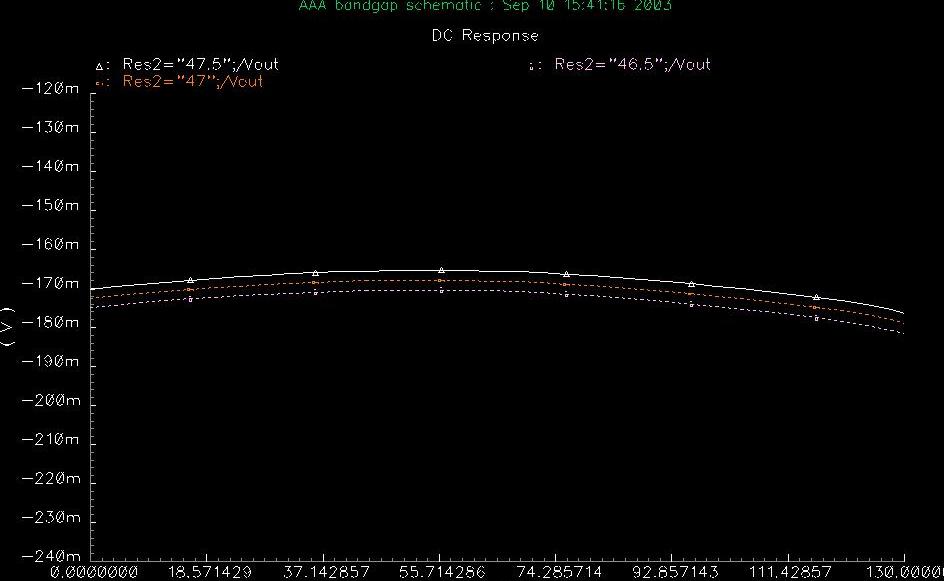
23 By clicking on Open, the Calculator will open Figure 37 By clicking on OP see a list of variables and then selecting the device from the schematic view, you will Figure 38 23
24 Figure 39 24
25 After selecting the variables to be plot, then just click on ERPLOT in the Calculator to plot. Figure 39 The waveform will look like: 25

26 Figure 40 26
27 Figure 41 27
28 Variation of the Bandgap Reference Voltage with respect to Temperature The example below is the classical Widlar Bandgap Voltage Reference Figure 42 28
29 By clicking on Tools -> Analog Environment Figure 43. The type of analysis is dc as in Figure

30 Figure 44 30

31 The output signals to be observed during the simulation are: Figure 45 To start simulation from click on Netlist and Run Figure 46 31
32 The waveforms for the output signals as we perform dc analysis on variable temperature: Figure 47 32
")
33 Bandgap Temperature Reference (Version 2) Figure 48 33
34 Figure 49 34

35 Figure 50 35
36 Single Stage Amplifiers Figure 51 This is a common-source single-transistor amplifier. 36
37 Type of analysis performed: Figure 52 37
38 There are two voltage variables set in this circuit. One is for the VDD voltage and the other is for Vin source. Figure 53 The output selected is as highlighted below: Figure 54 38
39 This is the waveform obtained form the common-source amplifier. This waveform plots the output versus the VDD range as Vin is varying from 0->2V. This waveform plots the Vin vs Vout as VDD varies. Figure 55 and 56 39
40 MOS Differential Amplifier with a Current Mirror Load Figure 57 This is a MOS current mirror load differential amplifier. 40
41 The type of analysis performed is DC. Figure 58 41
42 The analysis is performed on Variable V2 which is the input voltage. Figure 59 42
43 The variables used for this simulation are: Where V1 is for the input voltage and V2 is for the VDD voltage source. Check schematic for more information. Figure 60 The parametric analysis performed for variable V1 after performing Dc simulation. Figure 61 43
44 The waveform obtained looks like below. This waveform is Vin vs Vout plot. Figure 62 44

45 High Frequency Response in Diff. Pairs In order to estimate the frequency response of the differential pair with active current mirror the schematic model shown below is used where all capacitances are neglected. Figure 63 45
46 Performing Transient Analysis: The selected nets are input and output nets. Figure 64 Transient analysis is performed. 46

47 Figure 65 The waveforms obtained are: Figure 66 47
48 Noise in Differential Pairs Figure 67 This type of modeling accounts for 1/f noise and input-referred noise. 48
49 Performing Transient Analysis: Nets selected are input and output nets. Figure 68 Transient Analysis Figure 69 49
50 The waveforms obtained; Figure 70 50
DC Operating Point, I-V Curve Trace. Author: Nate Turner
 DC Operating Point, I-V Curve Trace Author: Nate Turner Description: This tutorial demonstrates how to print the DC-Operating Point as well as trace the I-V curves for a transistor in the tsmc 180nm process.
UNIVERSITY OF CALIFORNIA College of Engineering Department of Electrical Engineering and Computer Sciences
 UNIVERSITY OF CALIFORNIA College of Engineering Department of Electrical Engineering and Computer Sciences Jan M. Rabaey Homework #1: Circuit Simulation EECS 141 Due Friday, January 29, 5pm, box in 240
EECS 312: Digital Integrated Circuits Lab Project 1 Introduction to Schematic Capture and Analog Circuit Simulation
 EECS 312: Digital Integrated Circuits Lab Project 1 Introduction to Schematic Capture and Analog Circuit Simulation Teacher: Robert Dick GSI: Shengshuo Lu Assigned: 5 September 2013 Due: 17 September 2013
Introduction to PSpice
 Electric Circuit I Lab Manual 4 Session # 5 Introduction to PSpice 1 PART A INTRODUCTION TO PSPICE Objective: The objective of this experiment is to be familiar with Pspice (learn how to connect circuits,
Lab 2: Basic Boolean Circuits. Brittany Duffy EE 330- Integrated Electronics Lab Section B Professor Randy Geiger 1/31/13
 Lab 2: Basic Boolean Circuits Brittany Duffy EE 330- Integrated Electronics Lab Section B Professor Randy Geiger 1/31/13 Introduction The main goal of this lab was to become familiarized with the methods
EEC 116 Fall 2011 Lab #2: Analog Simulation Tutorial
 EEC 116 Fall 2011 Lab #2: Analog Simulation Tutorial Dept. of Electrical and Computer Engineering University of California, Davis Issued: September 28, 2011 Due: October 12, 2011, 4PM Reading: Rabaey Chapters
University of Michigan EECS 311: Electronic Circuits Fall 2008 LAB 4 SINGLE STAGE AMPLIFIER
 University of Michigan EECS 311: Electronic Circuits Fall 2008 LAB 4 SINGLE STAGE AMPLIFIER Issued 10/27/2008 Report due in Lecture 11/10/2008 Introduction In this lab you will characterize a 2N3904 NPN
ECEN 474/704 Lab 6: Differential Pairs
 ECEN 474/704 Lab 6: Differential Pairs Objective Design, simulate and layout various differential pairs used in different types of differential amplifiers such as operational transconductance amplifiers
ETI063 - Analogue IC Design Laboratory Manual
 Department of Electrical and Information Technology ETI063 - Analogue IC Design Laboratory Manual Ellie Cijvat September 2009 CONTENTS i Contents Introduction 1 Laboratory Overview........................
Faculty of Engineering 4 th Year, Fall 2010
 4. Inverter Schematic a) After you open the previously created Inverter schematic, an empty window appears where you should place your components. To place an NMOS, select Add- >Instance or use shortcut
Lab 2: Discrete BJT Op-Amps (Part I)
") Lab 2: Discrete BJT Op-Amps (Part I) This is a three-week laboratory. You are required to write only one lab report for all parts of this experiment. 1.0. INTRODUCTION In this lab, we will introduce and
Lab 2: Discrete BJT Op-Amps (Part I) This is a three-week laboratory. You are required to write only one lab report for all parts of this experiment. 1.0. INTRODUCTION In this lab, we will introduce and
EE 2274 RC and Op Amp Circuit Completed Prior to Coming to Lab. Prelab Part I: RC Circuit
 EE 2274 RC and Op Amp Circuit Completed Prior to Coming to Lab Prelab Part I: RC Circuit 1. Design a high pass filter (Fig. 1) which has a break point f b = 1 khz at 3dB below the midband level (the -3dB
Tutorial #5: Emitter Follower or Common Collector Amplifier Circuit
 Tutorial #5: Emitter Follower or Common Collector Amplifier Circuit This tutorial will help you to build and simulate a more complex circuit: an emitter follower. The emitter follower or common collector
Lab 3: Circuit Simulation with PSPICE
 Page 1 of 11 Laboratory Goals Introduce text-based PSPICE as a design tool Create transistor circuits using PSPICE Simulate output response for the designed circuits Introduce the Curve Tracer functionality.
ECE4902 Lab 5 Simulation. Simulation. Export data for use in other software tools (e.g. MATLAB or excel) to compare measured data with simulation
 to compare measured data with simulation") ECE4902 Lab 5 Simulation Simulation Export data for use in other software tools (e.g. MATLAB or excel) to compare measured data with simulation Be sure to have your lab data available from Lab 5, Common
ECE4902 Lab 5 Simulation Simulation Export data for use in other software tools (e.g. MATLAB or excel) to compare measured data with simulation Be sure to have your lab data available from Lab 5, Common
EXPERIMENT NUMBER 10 TRANSIENT ANALYSIS USING PSPICE
 EXPERIMENT NUMBER 10 TRANSIENT ANALYSIS USING PSPICE Objective: To learn to use a circuit simulator package for plotting the response of a circuit in the time domain. Preliminary: Revise laboratory 8 to
A Brief Handout for Introduction to
 A Brief Handout for Introduction to Electric cal Engineering Course This handout is a compilation of PSPICE, A Brief Primer, Department of Electrical and Systems Engineering, University of Pennsylvania
UNIVERSITY OF NORTH CAROLINA AT CHARLOTTE Department of Electrical and Computer Engineering
 UNIVERSITY OF NORTH CAROLINA AT CHARLOTTE Department of Electrical and Computer Engineering EXPERIMENT 8 MOSFET AMPLIFIER CONFIGURATIONS AND INPUT/OUTPUT IMPEDANCE OBJECTIVES The purpose of this experiment
ENGI0531 Lab 2 Tutorial
 ENGI0531 Lab 2 Tutorial Transient Analysis, Operating Points, Parameters and other miscellany Lakehead University Greg Toombs Winter 2009 1. Constructing the Circuit Copying a Cell View Start Cadence as
Introduction to LT Spice IV with Examples
 Introduction to LT Spice IV with Examples 400D - Fall 2015 Purpose Part of Electronics & Control Division Technical Training Series by Nicholas Lombardo The purpose of this document is to give a basic
ECEN 474/704 Lab 1: Introduction to Cadence & MOS Device Characterization
 ECEN 474/704 Lab 1: Introduction to Cadence & MOS Device Characterization Objectives Learn how to login on a Linux workstation, perform basic Linux tasks, and use the Cadence design system to simulate
Using LTspice a Short Intro with Examples
 Using LTspice a Short Intro with Examples LTspice, also called SwitcherCAD, is a powerful and easy to use schematic capture program and SPICE engine, which is a general-purpose circuit simulation program
Mentor Analog Simulators
 ENGR-434 Spice Netlist Syntax Details Introduction Rev 5/25/11 As you may know, circuit simulators come in several types. They can be broadly grouped into those that simulate a circuit in an analog way,
LAB-2 (Tutorial) Simulation of LNA (Cadence SpectreRF)
 Simulation of LNA (Cadence SpectreRF)") Spring 2006: RF CMOS Transceiver Design (TSEK-26) 1/18 Date: Student Name: Lab Supervisor: Personal Number: - Signature: Notes: LAB-2 (Tutorial) Simulation of LNA (Cadence SpectreRF) Prepared By Rashad.M.Ramzan
Spring 2006: RF CMOS Transceiver Design (TSEK-26) 1/18 Date: Student Name: Lab Supervisor: Personal Number: - Signature: Notes: LAB-2 (Tutorial) Simulation of LNA (Cadence SpectreRF) Prepared By Rashad.M.Ramzan
LT Spice Getting Started Very Quickly. First Get the Latest Software!
 LT Spice Getting Started Very Quickly First Get the Latest Software! 1. After installing LT Spice, run it and check to make sure you have the latest version with respect to the latest version available
Engineering 3821 Fall Pspice TUTORIAL 1. Prepared by: J. Tobin (Class of 2005) B. Jeyasurya E. Gill
 B. Jeyasurya E. Gill") Engineering 3821 Fall 2003 Pspice TUTORIAL 1 Prepared by: J. Tobin (Class of 2005) B. Jeyasurya E. Gill 2 INTRODUCTION The PSpice program is a member of the SPICE (Simulation Program with Integrated Circuit
Engineering 3821 Fall 2003 Pspice TUTORIAL 1 Prepared by: J. Tobin (Class of 2005) B. Jeyasurya E. Gill 2 INTRODUCTION The PSpice program is a member of the SPICE (Simulation Program with Integrated Circuit
EE 230 Lab Lab 9. Prior to Lab
 MOS transistor characteristics This week we look at some MOS transistor characteristics and circuits. Most of the measurements will be done with our usual lab equipment, but we will also use the parameter
EXPERIMENT 9 Problem Solving: First-order Transient Circuits
 EXPERIMENT 9 Problem Solving: First-order Transient Circuits I. Introduction In transient analyses, we determine voltages and currents as functions of time. Typically, the time dependence is demonstrated
University of Michigan EECS 311: Electronic Circuits Fall 2009 LAB 2 NON IDEAL OPAMPS
 University of Michigan EECS 311: Electronic Circuits Fall 2009 LAB 2 NON IDEAL OPAMPS Issued 10/5/2008 Pre Lab Completed 10/12/2008 Lab Due in Lecture 10/21/2008 Introduction In this lab you will characterize
EECS 312: Digital Integrated Circuits Lab Project 2 Extracting Electrical and Physical Parameters from MOSFETs. Teacher: Robert Dick GSI: Shengshuo Lu
 EECS 312: Digital Integrated Circuits Lab Project 2 Extracting Electrical and Physical Parameters from MOSFETs Teacher: Robert Dick GSI: Shengshuo Lu Due 3 October 1 Introduction In this lab project, we
VCO Design Using SpectreRF. SpectreRF Workshop. VCO Design Using SpectreRF MMSIM6.0USR2. November
 SpectreRF Workshop VCO Design Using SpectreRF MMSIM6.0USR2 November 2005 November 2005 1 Contents Voltage Controlled Oscillator Design Measurements... 3 Purpose... 3 Audience... 3 Overview... 3 Introduction
Short Channel Bandgap Voltage Reference
 Short Channel Bandgap Voltage Reference EE-584 Final Report Authors: Thymour Legba Yugu Yang Chris Magruder Steve Dominick Table of Contents Table of Figures... 3 Abstract... 4 Introduction... 5 Theory
Class #9: Experiment Diodes Part II: LEDs
 Class #9: Experiment Diodes Part II: LEDs Purpose: The objective of this experiment is to become familiar with the properties and uses of LEDs, particularly as a communication device. This is a continuation
ETIN25 Analogue IC Design. Laboratory Manual Lab 2
 Department of Electrical and Information Technology LTH ETIN25 Analogue IC Design Laboratory Manual Lab 2 Jonas Lindstrand Martin Liliebladh Markus Törmänen September 2011 Laboratory 2: Design and Simulation
Getting Started with Cadence
 Collège Militaire Royal du Canada (Cadence University Alliance Program Member) Départment de Génie Electrique et Informatique RMC Microelectronics Lab Cadence Series Getting Started with Cadence Tutorial
Getting Started with Qucs
 Getting Started with Qucs Graham Edge University of Toronto After downloading Qucs, installing it, and running for the first time you should see a window that looks something like this: The large yellow
.dc Vcc Ib 0 50uA 5uA
 EE 2274 BJT Biasing PreLab: 1. Common Emitter (CE) Transistor Characteristics curve Generate the characteristics curves for a 2N3904 in LTspice by plotting Ic by sweeping Vce over a set of Ib steps. Label
Improving Test Coverage and Eliminating Test Escapes Using Analog Defect Analysis
 Improving Test Coverage and Eliminating Test Escapes Using Analog Defect Analysis Art Schaldenbrand, Dr. Walter Hartong, Amit Bajaj, Hany Elhak, and Vladimir Zivkovic, Cadence While the analog and mixed-signal
Class #8: Experiment Diodes Part I
 Class #8: Experiment Diodes Part I Purpose: The objective of this experiment is to become familiar with the properties and uses of diodes. We used a 1N914 diode in two previous experiments, but now we
UNIVERSITI MALAYSIA PERLIS
 UNIVERSITI MALAYSIA PERLIS ANALOG ELECTRONICS II EKT 214 Semester II (2013/2014) EXPERIMENT # 4 OP-AMP (COMPARATOR BASICS) EXPERIMENT 4 Op-Amp (Comparator Basics) 1. OBJECTIVE: 1.1 To demonstrate the op-amp
Experiment #6: Biasing an NPN BJT Introduction to CE, CC, and CB Amplifiers
 SCHOOL OF ENGINEERING AND APPLIED SCIENCE DEPARTMENT OF ELECTRICAL AND COMPUTER ENGINEERING ECE 2115: ENGINEERING ELECTRONICS LABORATORY Experiment #6: Biasing an NPN BJT Introduction to CE, CC, and CB
Submission date: Wednesday 21/3/2018
 Faculty of Information Engineering & Technology Electrical & Electronics Department Course: Microelectronics Lab ELCT605 Spring 2018 Dr. Eman Azab Eng. Samar Shukry Analog Report 1, 2 DC, TRANSIENT, AND
NGSPICE- Usage and Examples
 NGSPICE- Usage and Examples Debapratim Ghosh deba21pratim@gmail.com Electronic Systems Group Department of Electrical Engineering Indian Institute of Technology Bombay February 2013 Debapratim Ghosh Dept.
Simulation using Tutorial Verilog XL Release Date: 02/12/2005
 Simulation using Tutorial - 1 - Logic Simulation using Verilog XL: This tutorial includes one way of simulating digital circuits using Verilog XL. Here we have taken an example of two cascaded inverters.
Problem three helps in changing the biasing of the circuit to operate at a lower VDD but it comes at a cost of increased power.
 Summary By Saad Bin Nasir HW#3 helps us learn the following key components Problem one helps us understand the distribution of vds on the output transistors of an amplifier. Improved biasing can be made
Course Project Topic: RF Down-Conversion Chain Due Dates: Mar. 27, Apr. 15 (Interim reports), May. 11 (Final report)
, May. 11 (Final report)") Course Project Topic: RF Down-Conversion Chain Due Dates: Mar. 27, Apr. 15 (Interim reports), May. 11 (Final report) 1 Objective The objective of this project is to familiarize the student with the trade-offs
Course Project Topic: RF Down-Conversion Chain Due Dates: Mar. 27, Apr. 15 (Interim reports), May. 11 (Final report) 1 Objective The objective of this project is to familiarize the student with the trade-offs
EE 330 Laboratory 8 Discrete Semiconductor Amplifiers
 EE 330 Laboratory 8 Discrete Semiconductor Amplifiers Fall 2018 Contents Objective:...2 Discussion:...2 Components Needed:...2 Part 1 Voltage Controlled Amplifier...2 Part 2 A Nonlinear Application...3
Course Project Topic: RF Down-Conversion Chain Due Dates: Mar. 24, Apr. 7 (Interim reports), Apr. 28 (Final report)
, Apr. 28 (Final report)") Course Project Topic: RF Down-Conversion Chain Due Dates: Mar. 24, Apr. 7 (Interim reports), Apr. 28 (Final report) 1 Objective The objective of this project is to familiarize the student with the trade-offs
Course Project Topic: RF Down-Conversion Chain Due Dates: Mar. 24, Apr. 7 (Interim reports), Apr. 28 (Final report) 1 Objective The objective of this project is to familiarize the student with the trade-offs
Basics of Analog Multiplexers 1. Exercises TI Precision Labs Op Amps
 Basics of Analog Multiplexers 1 Exercises TI Precision Labs Op Amps 1 VSS VDD 1. In the circuit below, one of the input channels of the MUX36S08 is fed with a 2V p-p sinewave signal. The output of the
Reading. Lecture 17: MOS transistors digital. Context. Digital techniques:
 Reading Lecture 17: MOS transistors digital Today we are going to look at the analog characteristics of simple digital devices, 5. 5.4 And following the midterm, we will cover PN diodes again in forward
DESIGN OF A FULLY DIFFERENTIAL HIGH-SPEED HIGH-PRECISION AMPLIFIER
 DESIGN OF A FULLY DIFFERENTIAL HIGH-SPEED HIGH-PRECISION AMPLIFIER Mayank Gupta mayank@ee.ucla.edu N. V. Girish envy@ee.ucla.edu Design I. Design II. University of California, Los Angeles EE215A Term Project
What is an Op-Amp? The Surface
 What is an Op-Amp? The Surface An Operational Amplifier (Op-Amp) is an integrated circuit that uses external voltage to amplify the input through a very high gain. We recognize an Op-Amp as a massproduced
DIGITAL VLSI LAB ASSIGNMENT 1
 DIGITAL VLSI LAB ASSIGNMENT 1 Problem 1: NMOS and PMOS plots using Cadence. In this exercise, you are required to generate both NMOS and PMOS I-V device characteristics (I/P and O/P) using Cadence (Use
Introduction to SPICE. Simulator of Electronic devices
 Introduction to SPICE Simulator of Electronic devices Main steps: Download Instalation Open OrCAD capture CIS Lite Create a circuit. Place parts. Design a Simulation Profile Run PSpice F11 View simulation
ECE 2274 Diode Basics and a Rectifier Completed Prior to Coming to Lab
 ECE 2274 Diode Basics and a Rectifier Completed Prior to Coming to Lab Perlab: Part I I-V Characteristic Curve for the 1. Construct the circuit shown in figure 1. Using a DC Sweep, simulate in LTspice
ENGR 201 Homework, Fall 2018
 Chapter 1 Voltage, Current, Circuit Laws (Selected contents from Chapter 1-3 in the text book) 1. What are the following instruments? Draw lines to match them to their cables: Fig. 1-1 2. Complete the
EDA-BASED DESIGN PRACTICAL LABORATORY SESSION No. 4
 LABORATOIRE DE SYSTEMES MICROELECTRONIQUES EPFL STI IMM LSM ELD Station nº 11 CH-1015 Lausanne Téléphone : Fax : E-mail : Site web : +4121 693 6955 +4121 693 6959 lsm@epfl.ch lsm.epfl.ch EDA-BASED DESIGN
Introduction to NI Multisim & Ultiboard Software version 14.1
 School of Engineering and Applied Science Electrical and Computer Engineering Department Introduction to NI Multisim & Ultiboard Software version 14.1 Dr. Amir Aslani August 2018 Parts Probes Tools Outline
0.85V. 2. vs. I W / L
 EE501 Lab3 Exploring Transistor Characteristics and Design Common-Source Amplifiers Lab report due on September 22, 2016 Objectives: 1. Be familiar with characteristics of MOSFET such as gain, speed, power,
EECE 488: Short HSPICE. Tutorial. Last updated by: Mohammad Beikahmadi January Original presentation by: Jack Shiah
 EECE 488: Short HSPICE Tutorial Last updated by: Mohammad Beikahmadi January 2012 Original presentation by: Jack Shiah SPICE? Simulation Program with Integrated Circuit Emphasis An open source analog circuit
RELEASE NOTES SIMETRIX 6.2 O VERVIEW WHAT S NEW GUI DVM SIMETRIX SIMULATOR SIMPLIS SIMULATOR SCRIPT LANGUAGE MODEL LIBRARY
 RELEASE NOTES SIMETRIX 6.2 O VERVIEW This document provides details of SIMetrix Version 6.2. WHAT S NEW GUI 1. Model selection by specification. Some types of library model can now be selected from their
EE 330 Laboratory 8 Discrete Semiconductor Amplifiers
 EE 330 Laboratory 8 Discrete Semiconductor Amplifiers Fall 2017 Contents Objective:... 2 Discussion:... 2 Components Needed:... 2 Part 1 Voltage Controlled Amplifier... 2 Part 2 Common Source Amplifier...
Introduction to SwitcherCAD
 Introduction to SwitcherCAD 1 PREFACE 1.1 What is SwitcherCAD? SwitcherCAD III is a new Spice based program that was developed for modelling board level switching regulator systems. The program consists
Introduction to Full-Custom Circuit Design with HSPICE and Laker
 Introduction to VLSI and SOC Design Introduction to Full-Custom Circuit Design with HSPICE and Laker Course Instructor: Prof. Lan-Da Van T.A.: Tsung-Che Lu Department of Computer Science National Chiao
MultiSim and Analog Discovery 2 Manual
 MultiSim and Analog Discovery 2 Manual 1 MultiSim 1.1 Running Windows Programs Using Mac Obtain free Microsoft Windows from: http://software.tamu.edu Set up a Windows partition on your Mac: https://support.apple.com/en-us/ht204009
TSEK03 LAB 1: LNA simulation using Cadence SpectreRF
 TSEK03 Integrated Radio Frequency Circuits 2018/Ted Johansson 1/26 TSEK03 LAB 1: LNA simulation using Cadence SpectreRF Ver. 2018-09-18 for Cadence 6 & MMSIM 14 Receiver Front-end LO RF Filter 50W LNA
Atypical op amp consists of a differential input stage,
 IEEE JOURNAL OF SOLID-STATE CIRCUITS, VOL. 33, NO. 6, JUNE 1998 915 Low-Voltage Class Buffers with Quiescent Current Control Fan You, S. H. K. Embabi, and Edgar Sánchez-Sinencio Abstract This paper presents
EECE 488: Short HSPICE Tutorial. Last updated by: Mohammad Beikahmadi January 2013
 EECE 488: Short HSPICE Tutorial Last updated by: Mohammad Beikahmadi January 2013 SPICE? Simulation Program with Integrated Circuit Emphasis An open source analog circuit simulator Predicts circuit behavior,
EE140: Lab 5, Project Week 2
 EE140: Lab 5, Project Week 2 VGA Op-amp Introduction For this lab, you will be developing the background and circuits that you will need to get your final project to work. You should do this with your
EE501 Lab 7 Opamp Measurement
 EE501 Lab 7 Opamp Measurement Report due: Nov. 6, 2014 Objective: 1. Understand basic opamp measurement circuits. 2. Build testbench circuits for opamp measurement. Tasks: Op amps are very high gain amplifiers
Gechstudentszone.wordpress.com
 UNIT 4: Small Signal Analysis of Amplifiers 4.1 Basic FET Amplifiers In the last chapter, we described the operation of the FET, in particular the MOSFET, and analyzed and designed the dc response of circuits
UNIVERSITY OF NORTH CAROLINA AT CHARLOTTE Department of Electrical and Computer Engineering
 UNIVERSITY OF NORTH CAROLINA AT CHARLOTTE Department of Electrical and Computer Engineering EXPERIMENT 7 BJT AMPLIFIER CONFIGURATIONS AND INPUT/OUTPUT IMPEDANCE OBJECTIVES The purpose of this experiment
1.3 An Introduction to WinSPICE
 Chapter 1 Introduction to CMOS Design 23 After the GDS file is generated, we can use the Gds2Tlc program to convert the GDS file back into TLC files. In the setups we must specify a directory where the
Operational Amplifiers: Theory and Design
 Operational Amplifiers: Theory and Design TU Delft, the Netherlands, November 6-10, 2017 All Rights Reserved 2017 MEAD Education SA 2017 TU Delft These lecture notes are solely for the use of the registered
Assignment 8 Analyzing Operational Amplifiers in MATLAB and PSpice
 ECEL 301 ECE Laboratory I Dr. A. Fontecchio Assignment 8 Analyzing Operational Amplifiers in MATLAB and PSpice Goal Characterize critical parameters of the inverting or non-inverting opampbased amplifiers.
University of Michigan EECS 311: Electronic Circuits Fall 2008 LAB 2 ACTIVE FILTERS
 University of Michigan EECS 311: Electronic Circuits Fall 2008 LAB 2 ACTIVE FILTERS Issued 9/22/2008 Pre Lab Completed 9/29/2008 Lab Due in Lecture 10/6/2008 Introduction In this lab you will design a
TTL LOGIC and RING OSCILLATOR TTL
 ECE 2274 TTL LOGIC and RING OSCILLATOR TTL We will examine two digital logic inverters. The first will have a passive resistor pull-up output stage. The second will have an active transistor and current
EE140: Lab 5, Project Week 2
 Introduction EE140: Lab 5, Project Week 2 VGA Op-amp Group Presentations: 4/13 and 4/14 in Lab Slide Submission: 4/15/17 (9 am) For this lab, you will be developing the background and circuits that you
SIMULATIONS WITH THE BOOST TOPOLOGY EE562: POWER ELECTRONICS I COLORADO STATE UNIVERSITY. Modified February 2006
 SIMULATIONS WITH THE BOOST TOPOLOGY EE562: POWER ELECTRONICS I COLORADO STATE UNIVERSITY Modified February 26 Page 1 of 24 PURPOSE: The purpose of this lab is to simulate the Boost converter using ORCAD
Document Name: Electronic Circuits Lab. Facebook: Twitter:
 Document Name: Electronic Circuits Lab www.vidyathiplus.in Facebook: www.facebook.com/vidyarthiplus Twitter: www.twitter.com/vidyarthiplus Copyright 2011-2015 Vidyarthiplus.in (VP Group) Page 1 CIRCUIT
Electronic Circuits EE359A
 Electronic Circuits EE359A Bruce McNair B206 bmcnair@stevens.edu 201-216-5549 1 Memory and Advanced Digital Circuits - 2 Chapter 11 2 Figure 11.1 (a) Basic latch. (b) The latch with the feedback loop opened.
Basic Circuits. Current Mirror, Gain stage, Source Follower, Cascode, Differential Pair,
 Basic Circuits Current Mirror, Gain stage, Source Follower, Cascode, Differential Pair, CCS - Basic Circuits P. Fischer, ZITI, Uni Heidelberg, Seite 1 Reminder: Effect of Transistor Sizes Very crude classification:
7. Bipolar Junction Transistor
 41 7. Bipolar Junction Transistor 7.1. Objectives - To experimentally examine the principles of operation of bipolar junction transistor (BJT); - To measure basic characteristics of n-p-n silicon transistor
EE 320 L LABORATORY 9: MOSFET TRANSISTOR CHARACTERIZATIONS. by Ming Zhu UNIVERSITY OF NEVADA, LAS VEGAS 1. OBJECTIVE 2. COMPONENTS & EQUIPMENT
 EE 320 L ELECTRONICS I LABORATORY 9: MOSFET TRANSISTOR CHARACTERIZATIONS by Ming Zhu DEPARTMENT OF ELECTRICAL AND COMPUTER ENGINEERING UNIVERSITY OF NEVADA, LAS VEGAS 1. OBJECTIVE Get familiar with MOSFETs,
Mor M. Peretz Power Electronics Laboratory Department of Electrical and Computer Engineering Ben-Gurion University of the Negev, ISRAEL
 Mor M. Peretz Power Electronics Laboratory Department of Electrical and Computer Engineering Ben-Gurion University of the Negev, ISRAEL [1] PSpice A/D simulation program allows to analyze electrical circuits
EE 210 Lab Exercise #5: OP-AMPS I
 EE 210 Lab Exercise #5: OP-AMPS I ITEMS REQUIRED EE210 crate, DMM, EE210 parts kit, T-connector, 50Ω terminator, Breadboard Lab report due at the ASSIGNMENT beginning of the next lab period Data and results
ECE 310L : LAB 9. Fall 2012 (Hay)
") ECE 310L : LAB 9 PRELAB ASSIGNMENT: Read the lab assignment in its entirety. 1. For the circuit shown in Figure 3, compute a value for R1 that will result in a 1N5230B zener diode current of approximately
ECE 310L : LAB 9 PRELAB ASSIGNMENT: Read the lab assignment in its entirety. 1. For the circuit shown in Figure 3, compute a value for R1 that will result in a 1N5230B zener diode current of approximately
SAMPLE FINAL EXAMINATION FALL TERM
 ENGINEERING SCIENCES 154 ELECTRONIC DEVICES AND CIRCUITS SAMPLE FINAL EXAMINATION FALL TERM 2001-2002 NAME Some Possible Solutions a. Please answer all of the questions in the spaces provided. If you need
Microelectronics Circuit Analysis and Design. Differential Amplifier Intro. Differential Amplifier Intro. 12/3/2013. In this chapter, we will:
 Microelectronics Circuit Analysis and Design Donald A. Neamen Chapter 11 Differential Amplifiers In this chapter, we will: Describe the characteristics and terminology of the ideal differential amplifier.
Simulating Circuits James Lamberti 5/4/2014
 Simulating Circuits James Lamberti (jal416@lehigh.edu) 5/4/2014 There are many simulation and design platforms for circuits. The two big ones are Altium and Cadence. This tutorial will focus on Altium,
LNA Design Using SpectreRF. SpectreRF Workshop. LNA Design Using SpectreRF MMSIM6.0USR2. November
 SpectreRF Workshop LNA Design Using SpectreRF MMSIM6.0USR2 November 2005 November 2005 1 Contents Lower Noise Amplifier Design Measurements... 3 Purpose... 3 Audience... 3 Overview... 3 Introduction to
Common Mode Feedback for Fully Differential Amplifier in ami06 micron CMOS process
 Published by : http:// Common Mode Feedback for Fully Differential Amplifier in ami06 micron CMOS process Ravi Teja Bojanapally Department of Electrical and Computer Engineering, Texas Tech University,
Elad Alon HW #1: Circuit Simulation EECS 141 Due Thursday, Aug. 30th, 5pm, box in 240 Cory
 UNIVERSITY OF CALIFORNIA College of Engineering Department of Electrical Engineering and Computer Sciences Last modified on August 20, 2012 by Elad Alon Elad Alon HW #1: Circuit Simulation EECS 141 Due
Well we know that the battery Vcc must be 9V, so that is taken care of.
 HW 4 For the following problems assume a 9Volt battery available. 1. (50 points, BJT CE design) a) Design a common emitter amplifier using a 2N3904 transistor for a voltage gain of Av=-10 with the collector
Design and Simulation of RF CMOS Oscillators in Advanced Design System (ADS)
") Design and Simulation of RF CMOS Oscillators in Advanced Design System (ADS) By Amir Ebrahimi School of Electrical and Electronic Engineering The University of Adelaide June 2014 1 Contents 1- Introduction...
Design and Simulation of RF CMOS Oscillators in Advanced Design System (ADS) By Amir Ebrahimi School of Electrical and Electronic Engineering The University of Adelaide June 2014 1 Contents 1- Introduction...
OrCAD 17.2 Pspice Tutorial. High-Speed Circuits & Systems Lab. Yonsei University
 OrCAD 17.2 Pspice Tutorial High-Speed Circuits & Systems Lab. Yonsei University Installation Move to http://www.orcad.com/resources/orcaddownloads#demo Installation Click Download FREE-OrCAD 17.2 Lite
ENEE307 Lab 7 MOS Transistors 2: Small Signal Amplifiers and Digital Circuits
 ENEE307 Lab 7 MOS Transistors 2: Small Signal Amplifiers and Digital Circuits In this lab, we will be looking at ac signals with MOSFET circuits and digital electronics. The experiments will be performed
ET 304A Laboratory Tutorial-Circuitmaker For Transient and Frequency Analysis
 ET 304A Laboratory Tutorial-Circuitmaker For Transient and Frequency Analysis All circuit simulation packages that use the Pspice engine allow users to do complex analysis that were once impossible to
Basic Layout Techniques
 Basic Layout Techniques Rahul Shukla Advisor: Jaime Ramirez-Angulo Spring 2005 Mixed Signal VLSI Lab Klipsch School of Electrical and Computer Engineering New Mexico State University Outline Transistor
The default account setup for the class should allow you to run HSPICE without any further configuration. To verify this, type:
 UNIVERSITY OF CALIFORNIA College of Engineering Department of Electrical Engineering and Computer Sciences HW #1: Circuit Simulation NTU IC541CA (Spring 2004) 1 Objective The objective of this homework