CHAPTER 3 NEW SLEEPY- PASS GATE
|
|
|
- Claribel O’Connor’
- 5 years ago
- Views:
Transcription
1 56 CHAPTER 3 NEW SLEEPY- PASS GATE 3.1 INTRODUCTION A circuit level design technique is presented in this chapter to reduce the overall leakage power in conventional CMOS cells. The new leakage po leepy- es on static power dissipation in standby mode of operation using sleep transistors in pass gate (transmission gate) structure. However, unlike the sleep transistor technique, the Sleepy-pass gate technique retains the exact logic state; and, unlike the LECTOR technique, the Sleepy-pass gate technique can utilize high V th transistors with 180X (or greater compared with CMOS NAND gate at 100nm process) leakage savings. Therefore, far better than many prior approaches, the Sleepy-pass gate technique can achieve ultra low leakage power consumption while saving state. First, the structure of the Sleepy-pass gate technique is explained using a two input NAND gate. Then the detail of Sleepy-pass gate operation is described in active mode and sleep (standby) mode. 3.2 SLEEPY-PASS GATE Structure of Sleepy-pass Gate The Figure 3.1 represents a pair of complementary MOS transistors connected in parallel known as the CMOS pass gate (transmission gate)
2 57 configuration, which pass both 0 and 1 well. When the sleep signal on gate terminal of PMOS is a Logic 0, then its complement sleep_bar (Logic 1) is applied to gate terminal of NMOS, allowing both transistors to conduct and pass the signal at IN to OUT. When the sleep signal on gate terminal of PMOS is a Logic 1, complementary Logic 0 is applied to NMOS gate, turning both transistors off and forcing a high-impedance condition on both IN and OUT nodes. This high-impedance condition represents third "state" (high, low, or high-z). Thus, pass gate acts as an open circuit offering high resistance. This design acts as a voltage controlled resistor connecting input and output providing true bidirectional connectivity without degradation of the input signal. Figure 3.1 Pass gate (transmission gate) logic The Figure 3.2 plots ON resistance (R ON ) of pass gate as input voltage is swept from Gnd to V DD, assuming the output voltage closely follows. The effective ON resistance is a parallel combination of two resistances and is relatively constant across full range of input voltages. However the OFF resistance is very high and it is in the range of several mega ohms.
3 58 Figure 3.2 ON resistance of pass gate (Weste 2005) The sleep transistor concept used for dynamic circuits in (Kursun 2004) was adapted and modified to work for leakage reduction in static CMOS complementary circuits. A combination of high V th and standard V th sleep transistors are used in implementation (Lakshmikanthan 2006), to provide a well balanced trade-off between high speed and leakage loss. The proposed technique facilitates in the creation of an ultra low power standard cell library, using sleep-circuitry embedded components. Figure 3.3 illustrates the topology of a generic CMOS complementary circuit with Sleepyinputs, input 1, input 2...input n, feeding the Pull-Up Network (PUN) as well as the Pull-Down Network (PDN). The transistors in both the PUN and PDN are standard V th devices. The sleep circuitry consists of two transistors, one PMOS device S1 and one NMOS device S2. Transistors S1 and S2 are high
4 59 V th devices. The sleep transistors S1 and S2 are connected in parallel to form pass gate (transmission gate) configuration between PUN and PDN as shown in Figure 3.3 feed the gates of S1 and S2 respectively. The CMOS circuit output can be drawn either between PUN and sleep circuit or between sleep circuit and PDN. Figure 3.3 Block diagram of generic Sleepy-pass gate CMOS circuit Sleepy-pass Gate Operation The working of the Sleepy-pass gate CMOS circuit is discussed in this section. The sleep transistors S1 and S2 shown in Figure 3.3 are turned on during active mode and turned OFF during sleep mode. During the normal transistors S1 and S2 to turn ON and acts as a pass gate. The circuit behaves as a normal CMOS circuit without any hindrance from the sleep circuit. This can be seen from the DC characteristics obtained from HSPICE simulations.
5 60 Figure 3.4 shows a two input NAND gate with Sleepy-pass gate embedded. Figure 3.5 shows the DC characteristics of the NAND gate with the proposed method (the input A is fixed at 1 V and B is varied from 0 to 1 V). Figure 3.4 Two input NAND gate with Sleepy-pass gate structure Figure 3.5 DC characteristic of a two input NAND with Sleepy-pass gate
6 61 The ON resistance of the pass gate will be constant and lesser than its OFF resistance, allowing conduction between PUN and PDN. Even though the ON resistance of pass gate is not as high as its OFF state resistance, it increases the resistance of V DD to ground path, controlling the flow of leakage currents, resulting in leakage power reduction in active mode. In standby S2 to turn OFF forcing a high-impedance condition between PUN and PDN nodes. Thus, the introduction of Sleepy- pass gate increases the resistance of the path from V DD to ground during standby mode of operation resulting in reduction of leakage current. The leakage reduction of the Sleepy-pass gate structure occurs in two ways. First, leakage power is suppressed by high V th transistors, which are applied to the sleep transistors and the transistors parallel to the sleep transistors. Second, increases the resistance of the path from V DD to ground during standby mode, which also suppresses leakage power consumption. By combining these two effects, the Sleepy-pass gate structure achieves ultra low leakage power consumption during sleep mode while retaining exact logic state. Figure 3.6 shows the input-output curves of the NAND gate with proposed method simulated for 100-nm technology at 1V supply voltage. It can be observed from the curves that the proposed NAND gate produces exact output logic levels. For any given process technology, the standard V th transistors are unit-sized devices (the smallest width to length W/L ratio as defined by the technology). However, the high V th transistors S1 and S2 needs to be sized appropriately for the Sleepy-pass gate embedded CMOS cells to have a propagation delay comparable to that of the standard cells.


7 62 Figure 3.6 Input - output waveforms of a two input NAND with proposed method There is a nominal increase in both area and propagation delay of the Sleepy-pass gate embedded circuit, when compared to the standard CMOS circuits. This overhead of Sleepy-pass gate embedded cells is tradedoff against enormous power savings, when compared to the standard CMOS cells. In addition to that, output logic state is not lost when the circuit enters from mode to sleep mode and vice-versa. This seems attractive in comparison with some of the existing ways to use far lower V DD values and additional transistors to maintain logic state. Flautner (2002) also propose that some reduced V DD values sufficient to maintain the logic state. As an alternative option, the Sleepy-pass gate could be used between the supply voltage V DD and PUN and/or PDN and ground during active mode of operation. This will create virtual supply and/or ground rails. During standby mode, all sleep transistors are off, thus the actual power and
8 63 ground path are broken and the circuit experiences lower voltage. A very high resistance path is established between V DD and ground due to the parallel combination of the off resistance of sleep transistors and the leakage current flowing through the circuit reduces significantly and hence lowest power dissipation. 3.3 EVALUATION OF SLEEPY-PASS GATE TECHNIQUE The Sleepy-pass gate technique is evaluated by applying it for logic circuits, benchmark circuits and comparing with other existing well known techniques with HSPICE simulation/experimental setup shown in Figure 3.7. Figure 3.7 Experimental setup Simulation Setup In order to compare the results of the Sleepy-pass gate method with the base case, an experiment was carried out with a set of combinational logic gates. The schematics are designed for all the mentioned techniques using extracted from the schematics are modified with respect to the Berkeley
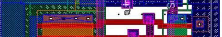
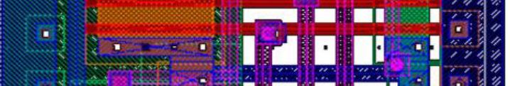
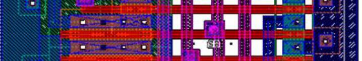
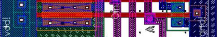
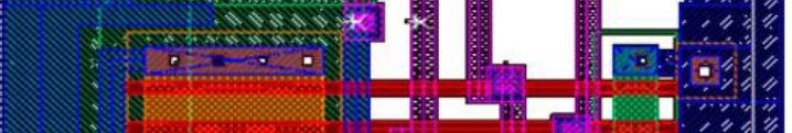
9 64 Predictive Technology Models. The modified netlists are simulated using Synopsys HSPICE for power and delay measurements Applying Sleepy-pass Gate for Logic Circuits Various circuit applications of the Sleepy-pass gate technique are explored. The generic logic circuits including inverter, NAND2, NOR2, AND2, OR2, multiplexer and full adder gates are implemented using state empirical saving as well as state-destructive low leakage techniques for evaluation. Detailed experimental methodology is explained. All circuits were simulated at a temperature of 25 C. Standard combinational CMOS library cells, such as NOR2, NAND2, OR2, AND2, XOR2, XNOR2 and MUX2x1, were implemented (Sahni 2006) using and modified accordingly for respective process technologies. Transistor sizes in all these circuits were fixed, and taken as PMOS width W P = 2 NMOS width W N = 1 L=100nm. A supply voltage (V DD ) of 1V was used and transient analysis performed on all 7 cells listed above, using HSPICE. The output load for each of the 7 cells was a capacitor of 1pF Simulation results for logic gates The total area of each standard cell in CMOS base case and proposed method is listed in Table 3.1. There is a slight increase in area for the proposed technique compared with base case due to additional transistors. Figure 3.8 and Figure 3.9 shows the layout for basic NAND and NOR gates for example. The propagation delay of each cell was measured for the purpose of comparing between base case and Sleepy-pass gate embedded cells. Next, the circuits were simulated at a temperature of 25 o C and their leakage power measured. All possible input combinations were applied and leakage power loss measured in every case. Column 2 of Table 3.2 lists the average leakage power loss for each standard CMOS cell.


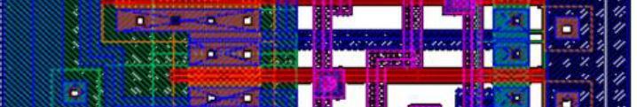
10 65 Figure 3.8 Two input CMOS NAND gate layout Next, the Sleepy-pass gate circuitry was introduced for all 7 standard CMOS cells. The sleep transistors S1 and S2 are unit sized as W S1 = W S2 100nm process technology. For each cell, transient analysis was performed in the normal mode of operatio _ propagation delays were calculated and compared to the standard circuit values as shown in Figure Figure 3.9 Two input NOR gate layout
 were sized such that the propagation delay of the Sleepy-pass gate cell was comparable to that of the standard")
11 66 Figure 3.10 Propagation delay with V DD =1 V The high V th sleep transistor(s) were sized such that the propagation delay of the Sleepy-pass gate cell was comparable to that of the standard cell. The Figure 3.10 shows that there is an increased delay for proposed technique compared to base case due to additional transistors. Finally, the Sleepy-pass gate embedded cell was simulated in the sleep (standby) mode of operation _ 3 of Table 3.2 lists the leakage power loss for all the Sleepy-pass gate embedded standard cells. Column 4 of Table 3.2 gives folds of leakage power savings on using the Sleepy-pass gate on combinational cells. Table 3.1 Area measurements for combinational 100nm process Area (µm 2 ) CMOS Gate Base Case Sleepy-pass Gate 2 input NAND input NOR input XOR input AND input OR input MUX bit Full Adder
12 67 Table 3.2 Leakage power for combinational 100nm process Average Leakage Power (W) with V DD = 1 Volt CMOS Gate Base Case Sleepy-pass Gate Leakage Savings 2 input NAND E E X 2 input NOR E E X 2 input XOR E E X 2 input AND E E X 2 input OR E E X 2 input MUX E E X 1-bit Full Adder E E X Increase in dynamic power dissipation The main emphasis till now has been on the standby (sleep) mode leakage power loss of the Sleepy-pass gate embedded cells. The dynamic power loss of these circuits has not been explored as yet. The dynamic power dissipation depends mainly on transient switching activity and frequency of operation, as well as on the square of the supply voltage. In this section, the effect of the additional sleep circuitry components on dynamic power dissipation of standard cells is studied. The combinational standard library cells were used, and their dynamic power measured. Table 3.3 gives the dynamic power dissipation comparison between standard CMOS cells (base case) and Sleepy-pass gate embedded cells. Column 2 of Table 3.3 gives the dynamic power loss of standard CMOS cells. Column 3 of Table 3.3 lists the dynamic power dissipation of the Sleepy-pass gate embedded cells. Analysis of results in Table 3.3 shows that the dynamic power penalty (increase) of the Sleepy-pass gate embedded, when compared to that of standard cells is due to the additional transistors introduced and the consequent capacitive increase in the sleep-embedded circuits.
13 68 Table 3.3 Dynamic power for combinational process Dynamic Power ( E -06 V DD =1V Combinational Cells Base Case Sleepy-pass Gate 2 input NAND input NOR input XOR input AND input OR input MUX bit Full Adder The literature detailing various methods to reduce dynamic power has been analyzed and can be summarized as follows: Clock and Signal Gating This is the simplest and most straight forward method to reduce transient switching activity of the highly active nodes in a circuit. Control signal gating techniques, like those presented by Kapadia (1999), target reduction in switching power. Operand Isolation Techniques The input sharing problem is typically the cause of unnecessary switching activity in modules where there should be none. Consider a simple Arithmetic and Logic Unit (ALU) designed for 4 operations (add, subtract, multiply and shift), all sharing 2 input signals - shifter units are simultaneously active along with the subtractor, thereby
14 69 wasting power. Operand isolation techniques, like using multiplexers or using multiple registers to drive different modules, solve the input-sharing problem. However, this increases the area and the delay, and adds other overheads. Transistor Re-ordering Techniques Hossain (1996) used a probability based transistor re-ordering technique to reduce dynamic power dissipation in CMOS circuits. Circuits Comprised of Independent Voltage Islands Lackey (2002) presented a comprehensive background on methods used to design voltage islands. They present various voltage island scenarios, a system architecture and chip implementation methodology, which are used to reduce active and static power consumption in SOC designs. The design implications of voltage islands are also evaluated. Carballo (2003) proposed a semi-custom voltage island approach to build high-speed serial links. Their approach is a mixture of selective custom design and the transparent use of multiple supplies to reduce power. The digital circuitry on the chip runs at a low supply voltage, while the analog circuitry runs at a higher voltage level. An on-chip regulator converts low to high voltage, and vice-versa. MTCMOS transistors are used in the custom design process. Hillman (2005) focused on minimizing the operating voltage to reduce dynamic power. The library of components created was characterized for different voltages. Next, the whole SOC design was built with various components from this library, using voltage level-shifting circuits and voltage isolation cells.
15 70 Hung (2005) presented a voltage island partitioning and floor planning algorithm for architecting SOC designs. Their work explores the thermal impact of voltage islands. A hybrid optimization approach consisting of a genetic algorithm based (GA-based) voltage island partitioning algorithm and a simulated annealing based (SA-based) floor-planning algorithm, is presented Applying Sleepy-pass Gate for Benchmark Circuits The ISCAS'85 benchmark circuits are ten combinational networks provided to authors at the 1985 International Symposium on Circuits and Systems. They subsequently have been used by many researchers as a basis for comparing results in several areas of digital design, including test generation, timing analysis, and technology mapping. Experiments were conducted on a variety of combinational multi implemented using various deep submicron process technologies. The HSPICE simulator, in conjunction with the BPTM deep submicron technology, was used to simulate circuits and to estimate leakage power dissipation. All circuits (unless specified otherwise) were simulated at a temperature of 25 o C. The Berkeley Predictive Technology Models (BPTM) contained process parameters and values only for standard V th PMOS and NMOS transistors. No models are available for high V th transistors. Except the Sleepy-pass gate transistors, the width for all other transistors are taken as W p = 3 µm and W n =1µm for PMOS and NMOS respectively. Experiments using some proprietary technology models obtained directly from foundries showed an interesting trend in the threshold voltage
16 71 value of high V th transistors. For a variety of deep-submicron technologies, we observed that the threshold voltage value of a high V th PMOS or a high V th NMOS transistor was 25%-35% more than that of a standard V th transistor. Hence, models for high V th PMOS and NMOS transistors were incorporated into BPTM with threshold voltage values 25% more than that of standard V th transistors. DC simulations were run using HSPICE to ensure that the threshold values of these high V th transistors were only 25% more than those of standard V th transistors. Table 3.4 and Table 3.5 lists the supply and threshold voltage values for various BPTM models for PMOS and NMOS transistors respectively. The first columns in Tables 3.4 and 3.5 list the technology feature size. The supply voltage used for each feature size is listed in Column 2 of both Table 3.4 and Table 3.5. Column 3 of Table 3.4 gives the threshold voltage of a standard PMOS transistor, while Column 3 of Table 3.5 gives the threshold voltage of a standard NMOS transistor. The threshold voltage of a high V th PMOS transistor is listed in Column 4 of Table 3.4 and the threshold voltage of a high V th NMOS transistor is listed in Column 4 of Table 3.5. Table 3.4 PMOS threshold voltage for BPTM models BPTM Process V DD PMOS Standard V th PMOS High V th 180nm 1.8V -0.42V -0.35V 130nm 1.3V -0.35V -0.32V 100nm 1.0V -0.30V -0.28V 70nm 0.85V -0.22V -0.18V
17 72 Table 3.5 NMOS threshold voltage for BPTM models BPTM Process V DD NMOS Standard V th NMOS High V th 180nm 1.8V 0.41V 0.55V 130nm 1.3V 0.33V 0.38V 100nm 1.0V 0.26V 0.34V 70nm 0.85V 0.21V 0.39V leakage values Ten experimental characteristics given in Table 3.6 with Sleepy-pass gate embedded. They were sized appropriately for 4 different deep-submicron technologies nm, 130 nm, 100nm and 70 nm. The PMOS and NMOS are sized with width to length ratio as W/L = 6 and W/L = 3 respectively except for the Sleepy-pass gates. Table 3.6 ISCAS '85 benchmark circuit characteristics Circuit Input Output Circuit Function Total Gates Name Lines Lines C432 Priority Decoder 160(18 XOR) 36 7 C Bit Single-Error- Correcting Circuit 202(104 XOR) C880 ALU and Control C1355 C Bit Single-Error- Correcting Circuit 16-bit error detector/ corrector C2670 ALU and Control C3540 ALU and Control C5315 ALU and Selector C bit Multiplier C7552 ALU and Control
18 73 The circuit C7552, containing approximately 3512 gates, is the largest design among all the benchmarks chosen, while circuit C432 is the smallest circuit with 160 gates. The supply voltages for the respective technologies are given in Column 2 of Table 3.4 and Table 3.5 for PMOS and NMOS respectively. Simulations were carried out, using HSPICE in the standby mode of operation, and their leakage loss measured. Since exhaustive testing for many of the benchmarks was impossible, a representative sample of randomly generated input vector combinations was applied to each of the circuits, and leakage loss was measured in every case. The average leakage power dissipation values are listed Table 3.7. Table 3.6 give the leakage values of the various benchmarks implemented using the 180 nm BPTM. Similarly, Column 3 give leakage values of the benchmarks for the 130 nm BPTM; Column 4 give leakage values of the benchmarks for the 100nm BPTM; and Column give leakage values of the benchmarks for the 70 nm BPTM. Table 3.7 R method rk circuits with proposed Circuits Leakage Power ( nw) 180-nm 130-nm 100-nm 70-nm C C C C C C C C C C
19 Prior Low Leakage Techniques Considered for Comparison Purposes The Sleepy-pass gate technique is compared to a conventional CMOS approach, which is the base case, and four other well-known previous approaches, i.e., the forced stack, sleep, zigzag and LECTOR techniques. The four bit adder circuit is chosen for implementation and comparison Four bit adder By use of the one bit full adder shown in Figure 3.11, four bit adder shown in Figure 3.12 is implemented. A full adder is an example of a typical complex CMOS gate. In Figure 3.11, a and b are two inputs and c is a carry input. Carry and Sum are outputs. The transistor sizing of the full adder is noted in Figure Figure 3.11 One bit full adder
20 75 Figure 3.12 Inputs of four bit adder Base case CMOS technique has shown in Figure 3.13 and described in a classic textbook by Weste (2005). Figure 3.13 shows a pull-up network and a pulldown network using as few transistors as possible to implement the Boolean logic function desired. The base case of a four bit adder is sized as explained in Section Figure 3.13 Base case
21 Forced stack technique Figure 3.14 shows the forced stack technique, which forces a stack structure by breaking down an existing transistor into two half size transistors. When the forced stack technique is applied, each existing transistor is replaced with two half sized transistors as shown in Figure Figure 3.14 Forced stack Sleep transistor technique The sleep transistor technique shown in Figure 3.15 uses sleep transistors between both V DD and the pull-up network as well as between Gnd and the pull-down network. Generally, the width/length (W/L) ratio is sized based on a trade-off between area, leakage reduction and delay. For simplicity, the sleep transistor is sized to the size of the largest transistor in the network (pull-up or pull-down) connected to the sleep transistor. The PMOS and NMOS sleep transistors have W/L = 6 and W/L = 3, respectively.
22 77 Figure 3.15 Sleep technique Zigzag The zigzag technique in Figure 3.16 uses one sleep transistor in each logic stage either in the pull-up or pull-down network according a particular input pattern. In this thesis, an input vector is used that can achieve the lowest possible leakage power consumption. Then, either assign a sleep transistor to the pull- it is assigned to the pull-. For Figure 3.16, it is assumed that the minimum leakage inputs are asserted. Therefore, a pull-down sleep transistor is assigned for the first stage and a pull-up sleep transistor for the second stage. Similar to the sleep transistor technique, the size of the sleep transistors are sized to that of the largest transistor in the network (pull-up or pull-down) connected to the sleep transistor. The PMOS and NMOS sleep transistors have W/L = 6 and W/L = 3, respectively.
23 78 Figure 3.16 Zigzag LECTOR LECTOR is an adaptation of the technique of effective stacking of transistors in order to reduce leakage power. Figure 3.17 shows the generic block diagram of a LECTOR CMOS circuit. Two Leakage Control Transistors (LTs), LT1 and LT2, are introduced between PUN and PDN. These LTs act as self-controlled stacked transistors. The LECTOR structure is shown in the Figure 3.17 where the LTs are unit sized with the ratio W/L = 6. Figure 3.17 Generic block diagram of LECTOR
24 Experiments on Sleepy-pass Gate Delay The worst case propagation delay of each benchmark is measured. Input vectors and input and output triggers are chosen to measure delay across trigger input edge reaching 50% of the supply voltage value and the circuit output edge reaching 50% of the supply voltage value. Input waveforms have a 4ns period (i.e., a 250 MHz rate) and rise and fall times of 100ps Active power Active power is measured by asserting semi-random input vectors and calculating the average power dissipation during this time. Input vectors are chosen so that a large number of possible input combinations are included in the set. The average power dissipation reported by HSPICE is taken as the estimate of active power consumption. This active power includes dynamic power as well as static power during the time measured. However, static power consumption is subtracted to calculate pure dynamic power consumption. All sleep transistors are turned on when active power is measured for the sleep, zigzag and Sleepy-pass gate techniques. For the four bit adder, input vectors covering every possible input are asserted. The waveform in Figure 3.18 shows input vectors asserted for each one bit adder, where the input vector changes in every 4ns. The same signal timing is used while scaling technology from 0.18 signal timing is not customized )
25 80 because in this way the effect of technology scaling on a fixed clock can be observed. However, it is known that reducing cycle time along with technology feature size is possible and may reveal additional insights and tradeoffs Static power HSPICE is also used to measure static power consumption. Since static power varies according to input state, either a full combination of input vectors or subset of possible input combinations is considered. When static power is measured, first an input vector is asserted and power consumption is measured after signals become stable (e.g., after 30ns). Each measured static power consumption over 30ns is averaged to derive static power consumption of each circuit. Figure 3.18 One bit adder input-output signals for dynamic power measurement For the four bit adder, all possible input vectors of a full adder are considered for leakage power measurement. The sleep transistors of the sleep,
26 81 zigzag and Sleepy-pass gate techniques are turned OFF during sleep mode in which the leakage power dissipation is measured Area particular design style (e.g., base case) is measured using layout. For a four bit adder, an actual full layout of adder is directly measured and estimated scaling the area of each benchmark layout for each particular design style Around 10% area overhead is added in order to consider non-linear 2 2 x (0.130/0.180) x 1.1 is estimated. m process, the area for To estimate technologies, extra area needed to wire gates is not taken into account but the absence of a wiring penalty equally affects all techniques considered (i.e, base case, sleep, forced stack, zigzag, LECTOR and Sleepy-pass gate). Figure 3.19 shows the layout of a full adder.


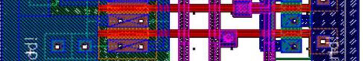
27 Figure 3.19 Layout of full adder 82
28 Comparative Results First the Sleepy-pass gate is compared to the base case and LECTOR techniques (self triggered sleep circuitry) in terms of leakage power and delay using a two input NAND gate at temperature 25 o C. Secondly with well-known techniques, i.e., sleep, zigzag, and forced stack, in terms of active power, leakage power, area and delay using four bit full adder circuit explained in Section Results of two input NAND gate Tables 3.8, 3.9 and 3.10 gives the leakage power, savings and delay penalty comparison for the base case, LECTOR and Sleepy-pass gate embedded NAND gates respectively. For a fair comparison, the supply voltage was set to 1V for the 100nm. In Table 3.8 the values reported in rows 3 list the leakage power values for a base case NAND gate, using BPTM 100nm. In Table 3.8 row 4 list the leakage values for the LECTOR NAND gate, using BPTM 100nm. Table 3.8 row 5 gives the leakage (in standby mode) values for the Sleepy-pass gate embedded NAND gate, using BPTM 100nm. Column 2 to column 5 of Table 3.8 indicates the corresponding input vectors applied to the gates. Analysis of the results in Table 3.8 shows that the leakage power is dependent on input vector applied to the circuits. (Abdollahi 2004). Column 2 and column 3 of Table 3.9 presents the average leakage power and leakage savings obtained for base case, LECTOR and Sleepy-pass gate NAND gates. It shows that the Sleepy-pass gate technique has the least leakage power dissipation and largest leakage savings of 180% when compared to the conventional CMOS NAND gate. Column 2 and column 3 of Table 3.10 gives the delay obtained by introducing the additional transistors and the corresponding delay penalty respectively. It shows that the
29 84 conventional NAND gate has the least propagation delay value compared to LECTOR and Sleepy-pass gate techniques. Also it is seen that the Sleepy-pass gate technique has less leakage power and reduced delay penalty than LECTOR at 100nm from Figure 3.20 and Figure Table 3.8 Leakage power comparison for two input NAND gate 100nm Process Technology with V DD = 1 Volt Leakage Power(W) for Input Vectors Method Base CMOS E E E E-07 Lector E E E E-09 Sleepy-pass gate E E E E-10 Table 3.9 Leakage power savings for two input NAND gate 100nm Process Technology with V DD = 1 Volt Method Average Leakage (W) Avgerage Leakage Savings Base CMOS 5.170E-08 - Lector E X Sleepy-pass gate E X Table 3.10 Delay penalty for two input NAND gate 100nm Process Technology with V DD = 1 Volt Method Delay (s) Delay Penalty% Base CMOS 1.3E-10 - Lector 1.8E Sleepy-pass gate 1.5E


30 85 Figure 3.20 Average leakage power for two input NAND gate Figure 3.21 Propagation delay for two input NAND gate Results of four bit full adder The impact of technology scaling is explored from the results of a four bit full adder in terms of static power, propagation delay, dynamic power
31 86 and area as tabulated in Table 3.11 to Table Table 3.11 gives the static power dissipation for 180nm, 130nm, 100nm and 70nm process technologies. Table 3.11 shows that the Sleepy-pass gate achieves large leakage reduction over the base case and the other compared leakage reduction techniques. From Figures 3.22, 3.23, 3.24 and 3.25 it is observed that static power increases as technology feature size shrinks. Table 3.12 gives the propagation delay of a four bit full adder implemented in base case as well as other leakage reduction techniques including Sleepy-pass gate at 180nm, 130nm, 100nm and 70nm process technologies. From Figure 3.26 it is observed that propagation delay decreases as technology feature size shrinks. Compared to the base case, Sleepy-pass gate has increasing delay and smaller when compared with LECTOR technique. Table 3.11 Static power dissipation for various process technologies Static Power (W) of Four Bit Full Adder 4-bit adder 180nm 130nm 100nm 70nm Base case 9.39E E E E-07 Forced stack 9.47E E E E-08 Sleep 7.28E E E E-07 Zigzag 4.28E E E E-08 LECTOR 8.11E E E E-08 Sleepy-pass gate 6.13E E E E-09
32 87 Table 3.12 Propogation delay for various process technologies Propagation Delay (s) of Four Bit Full Adder 4-bit Adder 180nm 130nm 100nm 70nm Base case 7.21E E E E-10 Forced stack 1.71E E E E-10 Sleep 1.12E E E E-10 Zigzag 1.12E E E E-10 LECTOR 1.39E E E E-10 Sleepy-pass gate 1.09E E E E-10 Table 3.13 gives the dynamic power dissipation of a four bit full adder at 180nm, 130nm, 100nm and 70nm process technologies. It is observed from Figure 3.27 that dynamic power decreases as technology feature size shrinks. Sleepy-pass gate has increased dynamic power dissipation compared to base case due to the additional sleep transistors used as sleep circuitry. Sleepy-pass gate has reduced dynamic power dissipation compared to zigzag and LECTOR techniques. From Table 3.14 and Figure 3.28, Sleepy-pass gate technique has increased area when compared to base case and decreases as technology feature size shrinks. Finally, compared to other techniques, the overhead of increased delay and area are judged to be worth. Therefore, our Sleepy-pass gate approach can be used where state preservation and ultra low leakage power consumption is needed and is judged to be worth the area overhead.
33 88 Table 3.13 Dynamic power dissipation for various process technologies Dynamic Power Dissipation (W) of Four Bit Full Adder 4-bit Adder 180nm 130nm 100nm 70nm Base case 4.81E E E E-05 Forced stack 5.70E E E E-05 Sleep 5.53E E E E-05 Zigzag 6.54E E E E-05 LECTOR 5.74E E E E-05 Sleepy-pass gate 5.66E E E E-05 Table 3.14 Area measured for various process technologies Area (µm 2 )of Four Bit Full Adder 4-bit Adder 180nm 130nm 100nm 70nm Base case Forced stack Sleep Zigzag LECTOR Sleepy-pass gate
34 89 Figure 3.22 Static power for four bit full adder at 180nm Figure 3.23 Static power for four bit full adder at 130nm
35 90 Figure 3.24 Static power for four bit full adder at 100nm Figure 3.25 Static power for four bit full adder at 70nm


36 91 Figure 3.26 Propagation delay for four bit full adder at various process technologies Figure 3.27 Dynamic power dissipation for four bit full adder at various process technologies
37 92 Figure 3.28 Area measured for four bit full adder at various process technologies 3.4 SUMMARY In this chapter, the Sleepy-pass gate structure was introduced and its operation for leakage power reduction is explained. The Sleepy-pass gate technique can achieve smaller transistor delay and larger leakage power savings than the other existing leakage reduction techniques compared. Scaling down of the CMOS technology feature size and threshold voltage for achieving high performance has resulted in increase of leakage power dissipation. This chapter presented an efficient methodology for reducing leakage power in CMOS VLSI design. Throughout logic design, the proposed method could be used to reduce the static power of CMOS circuits. Some of the implications in implementing this technique are as follows: Minimal additional circuitry is used to modify the original logic design to force the circuit into a low leakage state during standby mode of operation which can be a major implication in implementing this technique.
38 93 This technique requires a controller / power management system to automatically generate sleep signals during standby mode and also to activate it when necessary. There is a tradeoff between area, delay and power by utilizing this technique for power savings. DT-LECTOR is proposed in next chapter which could be used in applications that demand high speed and where sleep signal control circuitry is not available.
Novel Low-Overhead Operand Isolation Techniques for Low-Power Datapath Synthesis
 Novel Low-Overhead Operand Isolation Techniques for Low-Power Datapath Synthesis N. Banerjee, A. Raychowdhury, S. Bhunia, H. Mahmoodi, and K. Roy School of Electrical and Computer Engineering, Purdue University,
Ultra Low Power VLSI Design: A Review
 International Journal of Emerging Engineering Research and Technology Volume 4, Issue 3, March 2016, PP 11-18 ISSN 2349-4395 (Print) & ISSN 2349-4409 (Online) Ultra Low Power VLSI Design: A Review G.Bharathi
CHAPTER 3 PERFORMANCE OF A TWO INPUT NAND GATE USING SUBTHRESHOLD LEAKAGE CONTROL TECHNIQUES
 CHAPTER 3 PERFORMANCE OF A TWO INPUT NAND GATE USING SUBTHRESHOLD LEAKAGE CONTROL TECHNIQUES 41 In this chapter, performance characteristics of a two input NAND gate using existing subthreshold leakage
A Novel Low-Power Scan Design Technique Using Supply Gating
 A Novel Low-Power Scan Design Technique Using Supply Gating S. Bhunia, H. Mahmoodi, S. Mukhopadhyay, D. Ghosh, and K. Roy School of Electrical and Computer Engineering, Purdue University, West Lafayette,
LEAKAGE POWER REDUCTION IN CMOS CIRCUITS USING LEAKAGE CONTROL TRANSISTOR TECHNIQUE IN NANOSCALE TECHNOLOGY
 LEAKAGE POWER REDUCTION IN CMOS CIRCUITS USING LEAKAGE CONTROL TRANSISTOR TECHNIQUE IN NANOSCALE TECHNOLOGY B. DILIP 1, P. SURYA PRASAD 2 & R. S. G. BHAVANI 3 1&2 Dept. of ECE, MVGR college of Engineering,
ESTIMATION OF LEAKAGE POWER IN CMOS DIGITAL CIRCUIT STACKS
 ESTIMATION OF LEAKAGE POWER IN CMOS DIGITAL CIRCUIT STACKS #1 MADDELA SURENDER-M.Tech Student #2 LOKULA BABITHA-Assistant Professor #3 U.GNANESHWARA CHARY-Assistant Professor Dept of ECE, B. V.Raju Institute
A HIGH SPEED & LOW POWER 16T 1-BIT FULL ADDER CIRCUIT DESIGN BY USING MTCMOS TECHNIQUE IN 45nm TECHNOLOGY
 A HIGH SPEED & LOW POWER 16T 1-BIT FULL ADDER CIRCUIT DESIGN BY USING MTCMOS TECHNIQUE IN 45nm TECHNOLOGY Jasbir kaur 1, Neeraj Singla 2 1 Assistant Professor, 2 PG Scholar Electronics and Communication
Power-Area trade-off for Different CMOS Design Technologies
 Power-Area trade-off for Different CMOS Design Technologies Priyadarshini.V Department of ECE Sri Vishnu Engineering College for Women, Bhimavaram dpriya69@gmail.com Prof.G.R.L.V.N.Srinivasa Raju Head
CPE/EE 427, CPE 527 VLSI Design I: Homeworks 3 & 4
 CPE/EE 427, CPE 527 VLSI Design I: Homeworks 3 & 4 1 2 3 4 5 6 7 8 9 10 Sum 30 10 25 10 30 40 10 15 15 15 200 1. (30 points) Misc, Short questions (a) (2 points) Postponing the introduction of signals
Total reduction of leakage power through combined effect of Sleep stack and variable body biasing technique
 Total reduction of leakage power through combined effect of Sleep and variable body biasing technique Anjana R 1, Ajay kumar somkuwar 2 Abstract Leakage power consumption has become a major concern for
A Low Power Array Multiplier Design using Modified Gate Diffusion Input (GDI)
") A Low Power Array Multiplier Design using Modified Gate Diffusion Input (GDI) Mahendra Kumar Lariya 1, D. K. Mishra 2 1 M.Tech, Electronics and instrumentation Engineering, Shri G. S. Institute of Technology
A Low Power Array Multiplier Design using Modified Gate Diffusion Input (GDI) Mahendra Kumar Lariya 1, D. K. Mishra 2 1 M.Tech, Electronics and instrumentation Engineering, Shri G. S. Institute of Technology
Implementation of dual stack technique for reducing leakage and dynamic power
 Implementation of dual stack technique for reducing leakage and dynamic power Citation: Swarna, KSV, Raju Y, David Solomon and S, Prasanna 2014, Implementation of dual stack technique for reducing leakage
Design of low power SRAM Cell with combined effect of sleep stack and variable body bias technique
 Design of low power SRAM Cell with combined effect of sleep stack and variable body bias technique Anjana R 1, Dr. Ajay kumar somkuwar 2 1 Asst.Prof & ECE, Laxmi Institute of Technology, Gujarat 2 Professor
Digital Microelectronic Circuits ( ) CMOS Digital Logic. Lecture 6: Presented by: Adam Teman
 CMOS Digital Logic. Lecture 6: Presented by: Adam Teman") Digital Microelectronic Circuits (361-1-3021 ) Presented by: Adam Teman Lecture 6: CMOS Digital Logic 1 Last Lectures The CMOS Inverter CMOS Capacitance Driving a Load 2 This Lecture Now that we know all
Digital Microelectronic Circuits (361-1-3021 ) Presented by: Adam Teman Lecture 6: CMOS Digital Logic 1 Last Lectures The CMOS Inverter CMOS Capacitance Driving a Load 2 This Lecture Now that we know all
Study and Analysis of CMOS Carry Look Ahead Adder with Leakage Power Reduction Approaches
 Indian Journal of Science and Technology, Vol 9(17), DOI: 10.17485/ijst/2016/v9i17/93111, May 2016 ISSN (Print) : 0974-6846 ISSN (Online) : 0974-5645 Study and Analysis of CMOS Carry Look Ahead Adder with
Improved DFT for Testing Power Switches
 Improved DFT for Testing Power Switches Saqib Khursheed, Sheng Yang, Bashir M. Al-Hashimi, Xiaoyu Huang School of Electronics and Computer Science University of Southampton, UK. Email: {ssk, sy8r, bmah,
ZIGZAG KEEPER: A NEW APPROACH FOR LOW POWER CMOS CIRCUIT
 ZIGZAG KEEPER: A NEW APPROACH FOR LOW POWER CMOS CIRCUIT Kaushal Kumar Nigam 1, Ashok Tiwari 2 Department of Electronics Sciences, University of Delhi, New Delhi 110005, India 1 Department of Electronic
Minimizing the Sub Threshold Leakage for High Performance CMOS Circuits Using Stacked Sleep Technique
 International Journal of Electrical Engineering. ISSN 0974-2158 Volume 10, Number 3 (2017), pp. 323-335 International Research Publication House http://www.irphouse.com Minimizing the Sub Threshold Leakage
Domino Static Gates Final Design Report
 Domino Static Gates Final Design Report Krishna Santhanam bstract Static circuit gates are the standard circuit devices used to build the major parts of digital circuits. Dynamic gates, such as domino
On Chip Active Decoupling Capacitors for Supply Noise Reduction for Power Gating and Dynamic Dual Vdd Circuits in Digital VLSI
 ELEN 689 606 Techniques for Layout Synthesis and Simulation in EDA Project Report On Chip Active Decoupling Capacitors for Supply Noise Reduction for Power Gating and Dynamic Dual Vdd Circuits in Digital
Leakage Power Reduction for Logic Circuits Using Variable Body Biasing Technique
 Leakage Power Reduction for Logic Circuits Using Variable Body Biasing Technique Anjana R 1 and Ajay K Somkuwar 2 Assistant Professor, Department of Electronics and Communication, Dr. K.N. Modi University,
CHAPTER 5 DESIGN AND ANALYSIS OF COMPLEMENTARY PASS- TRANSISTOR WITH ASYNCHRONOUS ADIABATIC LOGIC CIRCUITS
 70 CHAPTER 5 DESIGN AND ANALYSIS OF COMPLEMENTARY PASS- TRANSISTOR WITH ASYNCHRONOUS ADIABATIC LOGIC CIRCUITS A novel approach of full adder and multipliers circuits using Complementary Pass Transistor
Topic 6. CMOS Static & Dynamic Logic Gates. Static CMOS Circuit. NMOS Transistors in Series/Parallel Connection
 NMOS Transistors in Series/Parallel Connection Topic 6 CMOS Static & Dynamic Logic Gates Peter Cheung Department of Electrical & Electronic Engineering Imperial College London Transistors can be thought
UNIT-III GATE LEVEL DESIGN
 UNIT-III GATE LEVEL DESIGN LOGIC GATES AND OTHER COMPLEX GATES: Invert(nmos, cmos, Bicmos) NAND Gate(nmos, cmos, Bicmos) NOR Gate(nmos, cmos, Bicmos) The module (integrated circuit) is implemented in terms
Design of 32-bit ALU using Low Power Energy Efficient Full Adder Circuits
 Design of 32-bit ALU using Low Power Energy Efficient Full Adder Circuits Priyadarshini.V Department of ECE Gudlavalleru Engieering College,Gudlavalleru darshiniv708@gmail.com Ramya.P Department of ECE
1. Short answer questions. (30) a. What impact does increasing the length of a transistor have on power and delay? Why? (6)
 a. What impact does increasing the length of a transistor have on power and delay? Why? (6)") CSE 493/593 Test 2 Fall 2011 Solution 1. Short answer questions. (30) a. What impact does increasing the length of a transistor have on power and delay? Why? (6) Decreasing of W to make the gate slower,
CSE 493/593 Test 2 Fall 2011 Solution 1. Short answer questions. (30) a. What impact does increasing the length of a transistor have on power and delay? Why? (6) Decreasing of W to make the gate slower,
Electronics Basic CMOS digital circuits
 Electronics Basic CMOS digital circuits Prof. Márta Rencz, Gábor Takács, Dr. György Bognár, Dr. Péter G. Szabó BME DED October 21, 2014 1 / 30 Introduction The topics covered today: The inverter: the simplest
Leakage Current Analysis
 Current Analysis Hao Chen, Latriese Jackson, and Benjamin Choo ECE632 Fall 27 University of Virginia , , @virginia.edu Abstract Several common leakage current reduction methods such
Leakage Power Reduction by Using Sleep Methods
 www.ijecs.in International Journal Of Engineering And Computer Science ISSN:2319-7242 Volume 2 Issue 9 September 2013 Page No. 2842-2847 Leakage Power Reduction by Using Sleep Methods Vinay Kumar Madasu
DFT for Testing High-Performance Pipelined Circuits with Slow-Speed Testers
 DFT for Testing High-Performance Pipelined Circuits with Slow-Speed Testers Muhammad Nummer and Manoj Sachdev University of Waterloo, Ontario, Canada mnummer@vlsi.uwaterloo.ca, msachdev@ece.uwaterloo.ca
A Literature Review on Leakage and Power Reduction Techniques in CMOS VLSI Design
 A Literature Review on Leakage and Power Reduction Techniques in CMOS VLSI Design Anu Tonk Department of Electronics Engineering, YMCA University, Faridabad, Haryana tonkanu.saroha@gmail.com Shilpa Goyal
Low Power Adiabatic Logic Design
 IOSR Journal of Electronics and Communication Engineering (IOSR-JECE) e-issn: 2278-2834,p- ISSN: 2278-8735.Volume 12, Issue 1, Ver. III (Jan.-Feb. 2017), PP 28-34 www.iosrjournals.org Low Power Adiabatic
SURVEY AND EVALUATION OF LOW-POWER FULL-ADDER CELLS
 SURVEY ND EVLUTION OF LOW-POWER FULL-DDER CELLS hmed Sayed and Hussain l-saad Department of Electrical & Computer Engineering University of California Davis, C, U.S.. STRCT In this paper, we survey various
A new 6-T multiplexer based full-adder for low power and leakage current optimization
 A new 6-T multiplexer based full-adder for low power and leakage current optimization G. Ramana Murthy a), C. Senthilpari, P. Velrajkumar, and T. S. Lim Faculty of Engineering and Technology, Multimedia
Low Power, Area Efficient FinFET Circuit Design
 Low Power, Area Efficient FinFET Circuit Design Michael C. Wang, Princeton University Abstract FinFET, which is a double-gate field effect transistor (DGFET), is more versatile than traditional single-gate
Subthreshold Voltage High-k CMOS Devices Have Lowest Energy and High Process Tolerance
 Subthreshold Voltage High-k CMOS Devices Have Lowest Energy and High Process Tolerance Muralidharan Venkatasubramanian Auburn University vmn0001@auburn.edu Vishwani D. Agrawal Auburn University vagrawal@eng.auburn.edu
II. Previous Work. III. New 8T Adder Design
 ISSN: 2277 128X International Journal of Advanced Research in Computer Science and Software Engineering Research Paper Available online at: High Performance Circuit Level Design For Multiplier Arun Kumar
ISSN:
 1061 Area Leakage Power and delay Optimization BY Switched High V TH Logic UDAY PANWAR 1, KAVITA KHARE 2 12 Department of Electronics and Communication Engineering, MANIT, Bhopal 1 panwaruday1@gmail.com,
ECE 334: Electronic Circuits Lecture 10: Digital CMOS Circuits
 Faculty of Engineering ECE 334: Electronic Circuits Lecture 10: Digital CMOS Circuits CMOS Technology Complementary MOS, or CMOS, needs both PMOS and NMOS FET devices for their logic gates to be realized
Implementation of Carry Select Adder using CMOS Full Adder
 Implementation of Carry Select Adder using CMOS Full Adder Smitashree.Mohapatra Assistant professor,ece department MVSR Engineering College Nadergul,Hyderabad-510501 R. VaibhavKumar PG Scholar, ECE department(es&vlsid)
Design and Implementation of ALU Chip using D3L Logic and Ancient Mathematics
 Design and Implementation of ALU Chip using D3L and Ancient Mathematics Mohanarangan S PG Student (M.E-Applied Electronics) Department of Electronics and Communicaiton Engineering Sri Venkateswara College
UNIT-II LOW POWER VLSI DESIGN APPROACHES
 UNIT-II LOW POWER VLSI DESIGN APPROACHES Low power Design through Voltage Scaling: The switching power dissipation in CMOS digital integrated circuits is a strong function of the power supply voltage.
MTCMOS Hierarchical Sizing Based on Mutual Exclusive Discharge Patterns
 MTCMOS Hierarchical Sizing Based on Mutual Exclusive Discharge Patterns James Kao, Siva Narendra, Anantha Chandrakasan Department of Electrical Engineering and Computer Science Massachusetts Institute
IC Layout Design of 4-bit Universal Shift Register using Electric VLSI Design System
 IC Layout Design of 4-bit Universal Shift Register using Electric VLSI Design System 1 Raj Kumar Mistri, 2 Rahul Ranjan, 1,2 Assistant Professor, RTC Institute of Technology, Anandi, Ranchi, Jharkhand,
Reduction Of Leakage Current And Power In CMOS Circuits Using Stack Technique
 International OPEN ACCESS Journal Of Modern Engineering Research (IJMER) Reduction Of Leakage Current And Power In CMOS Circuits Using Stack Technique Mansi Gangele 1, K.Pitambar Patra 2 *(Department Of
A Novel Dual Stack Sleep Technique for Reactivation Noise suppression in MTCMOS circuits
 IOSR Journal of VLSI and Signal Processing (IOSR-JVSP) Volume 3, Issue 3 (Sep. Oct. 2013), PP 32-37 e-issn: 2319 4200, p-issn No. : 2319 4197 A Novel Dual Stack Sleep Technique for Reactivation Noise suppression
High Performance Low-Power Signed Multiplier
 High Performance Low-Power Signed Multiplier Amir R. Attarha Mehrdad Nourani VLSI Circuits & Systems Laboratory Department of Electrical and Computer Engineering University of Tehran, IRAN Email: attarha@khorshid.ece.ut.ac.ir
A Low-Power High-speed Pipelined Accumulator Design Using CMOS Logic for DSP Applications
 International Journal of Research Studies in Computer Science and Engineering (IJRSCSE) Volume. 1, Issue 5, September 2014, PP 30-42 ISSN 2349-4840 (Print) & ISSN 2349-4859 (Online) www.arcjournals.org
Electronic Circuits EE359A
 Electronic Circuits EE359A Bruce McNair B206 bmcnair@stevens.edu 201-216-5549 1 Memory and Advanced Digital Circuits - 2 Chapter 11 2 Figure 11.1 (a) Basic latch. (b) The latch with the feedback loop opened.
A Low-Power SRAM Design Using Quiet-Bitline Architecture
 A Low-Power SRAM Design Using uiet-bitline Architecture Shin-Pao Cheng Shi-Yu Huang Electrical Engineering Department National Tsing-Hua University, Taiwan Abstract This paper presents a low-power SRAM
Sleepy Keeper Approach for Power Performance Tuning in VLSI Design
 International Journal of Electronics and Communication Engineering. ISSN 0974-2166 Volume 6, Number 1 (2013), pp. 17-28 International Research Publication House http://www.irphouse.com Sleepy Keeper Approach
CHAPTER 1 INTRODUCTION
 CHAPTER 1 INTRODUCTION 2 1.1 MOTIVATION FOR LOW POWER CIRCUIT DESIGN Low power circuit design has emerged as a principal theme in today s electronics industry. In the past, major concerns among researchers
A NEW APPROACH FOR DELAY AND LEAKAGE POWER REDUCTION IN CMOS VLSI CIRCUITS
 http:// A NEW APPROACH FOR DELAY AND LEAKAGE POWER REDUCTION IN CMOS VLSI CIRCUITS Ruchiyata Singh 1, A.S.M. Tripathi 2 1,2 Department of Electronics and Communication Engineering, Mangalayatan University
Low Power 8-Bit ALU Design Using Full Adder and Multiplexer
 Low Power 8-Bit ALU Design Using Full Adder and Multiplexer Gaddam Sushil Raj B.Tech, Vardhaman College of Engineering. ABSTRACT: Arithmetic logic unit (ALU) is an important part of microprocessor. In
A Novel Hybrid Full Adder using 13 Transistors
 A Novel Hybrid Full Adder using 13 Transistors Lee Shing Jie and Siti Hawa binti Ruslan Department of Electrical and Electronic Engineering, Faculty of Electric & Electronic Engineering Universiti Tun
A NOVEL 4-Bit ARITHMETIC LOGIC UNIT DESIGN FOR POWER AND AREA OPTIMIZATION
 A NOVEL 4-Bit ARITHMETIC LOGIC UNIT DESIGN FOR POWER AND AREA OPTIMIZATION Mr. Snehal Kumbhalkar 1, Mr. Sanjay Tembhurne 2 Department of Electronics and Communication Engineering GHRAET, Nagpur, Maharashtra,
Investigation on Performance of high speed CMOS Full adder Circuits
 ISSN (O): 2349-7084 International Journal of Computer Engineering In Research Trends Available online at: www.ijcert.org Investigation on Performance of high speed CMOS Full adder Circuits 1 KATTUPALLI
A Novel Multi-Threshold CMOS Based 64-Bit Adder Design in 45nm CMOS Technology for Low Power Application
 A Novel Multi-Threshold CMOS Based 64-Bit Adder Design in 45nm CMOS Technology for Low Power Application Rumi Rastogi and Sujata Pandey Amity University Uttar Pradesh, Noida, India Email: rumi.ravi@gmail.com,
Power Efficiency of Half Adder Design using MTCMOS Technique in 35 Nanometre Regime
 IJIRST International Journal for Innovative Research in Science & Technology Volume 1 Issue 12 May 2015 ISSN (online): 2349-6010 Power Efficiency of Half Adder Design using MTCMOS Technique in 35 Nanometre
IMPLEMENTATION OF POWER GATING TECHNIQUE IN CMOS FULL ADDER CELL TO REDUCE LEAKAGE POWER AND GROUND BOUNCE NOISE FOR MOBILE APPLICATION
 International Journal of Electronics, Communication & Instrumentation Engineering Research and Development (IJECIERD) ISSN 2249-684X Vol.2, Issue 3 Sep 2012 97-108 TJPRC Pvt. Ltd., IMPLEMENTATION OF POWER
P. Sree latha, M. Arun kumar
 International Journal of Scientific & Engineering Research Volume 9, Issue 3, March-2018 1 Performance Analysis of Comparator using Different Design Techniques P. Sree latha, M. Arun kumar Abstract - As
LOW POWER NOVEL HYBRID ADDERS FOR DATAPATH CIRCUITS IN DSP PROCESSOR
 LOW POWER NOVEL HYBRID ADDERS FOR DATAPATH CIRCUITS IN DSP PROCESSOR B. Sathiyabama 1, Research Scholar, Sathyabama University, Chennai, India, mathumithasurya@gmail.com Abstract Dr. S. Malarkkan 2, Principal,
Design and Analysis of CMOS based Low Power Carry Select Full Adder
 Design and Analysis of CMOS based Low Power Carry Select Full Adder Mayank Sharma 1, Himanshu Prakash Rajput 2 1 Department of Electronics & Communication Engineering Hindustan College of Science & Technology,
Low Power Design of Successive Approximation Registers
 Low Power Design of Successive Approximation Registers Rabeeh Majidi ECE Department, Worcester Polytechnic Institute, Worcester MA USA rabeehm@ece.wpi.edu Abstract: This paper presents low power design
International Journal of Engineering Trends and Technology (IJETT) Volume 45 Number 5 - March 2017
 Volume 45 Number 5 - March 2017") Performance Evaluation in Adiabatic Logic Circuits for Low Power VLSI Design Tabassum Ara #1, Amrita Khera #2, # PG Student [VLSI], Dept. of ECE, Trinity stitute of Technology and Research, Bhopal, RGPV
Performance Evaluation in Adiabatic Logic Circuits for Low Power VLSI Design Tabassum Ara #1, Amrita Khera #2, # PG Student [VLSI], Dept. of ECE, Trinity stitute of Technology and Research, Bhopal, RGPV
Reduced Swing Domino Techniques for Low Power and High Performance Arithmetic Circuits
 Reduced Swing Domino Techniques for Low Power and High Performance Arithmetic Circuits by Shahrzad Naraghi A thesis presented to the University of Waterloo in fulfillment of the thesis requirement for
ECE 683 Project Report. Winter Professor Steven Bibyk. Team Members. Saniya Bhome. Mayank Katyal. Daniel King. Gavin Lim.
 ECE 683 Project Report Winter 2006 Professor Steven Bibyk Team Members Saniya Bhome Mayank Katyal Daniel King Gavin Lim Abstract This report describes the use of Cadence software to simulate logic circuits
Design of Low power and Area Efficient 8-bit ALU using GDI Full Adder and Multiplexer
 Design of Low power and Area Efficient 8-bit ALU using GDI Full Adder and Multiplexer Mr. Y.Satish Kumar M.tech Student, Siddhartha Institute of Technology & Sciences. Mr. G.Srinivas, M.Tech Associate
A SUBSTRATE BIASED FULL ADDER CIRCUIT
 International Journal on Intelligent Electronic System, Vol. 8 No.. July 4 9 A SUBSTRATE BIASED FULL ADDER CIRCUIT Abstract Saravanakumar C., Senthilmurugan S.,, Department of ECE, Valliammai Engineering
International Journal of Advanced Research in Computer Science and Software Engineering
 Volume 3, Issue 8, August 2013 ISSN: 2277 128X International Journal of Advanced Research in Computer Science and Software Engineering Research Paper Available online at: www.ijarcsse.com A Novel Implementation
Figure.1. Schematic of 4-bit CLA JCHPS Special Issue 9: June Page 101
 Delay Depreciation and Power efficient Carry Look Ahead Adder using CMOS T. Archana*, K. Arunkumar, A. Hema Malini Department of Electronics and Communication Engineering, Saveetha Engineering College,
Low Power 32-bit Improved Carry Select Adder based on MTCMOS Technique
 Low Power 32-bit Improved Carry Select Adder based on MTCMOS Technique Ch. Mohammad Arif 1, J. Syamuel John 2 M. Tech student, Department of Electronics Engineering, VR Siddhartha Engineering College,
Enhancement of Design Quality for an 8-bit ALU
 ABHIYANTRIKI An International Journal of Engineering & Technology (A Peer Reviewed & Indexed Journal) Vol. 3, No. 5 (May, 2016) http://www.aijet.in/ eissn: 2394-627X Enhancement of Design Quality for an
DESIGN OF LOW POWER HIGH PERFORMANCE 4-16 MIXED LOGIC LINE DECODER P.Ramakrishna 1, T Shivashankar 2, S Sai Vaishnavi 3, V Gowthami 4 1
 DESIGN OF LOW POWER HIGH PERFORMANCE 4-16 MIXED LOGIC LINE DECODER P.Ramakrishna 1, T Shivashankar 2, S Sai Vaishnavi 3, V Gowthami 4 1 Asst. Professsor, Anurag group of institutions 2,3,4 UG scholar,
Comparative Study of Different Low Power Design Techniques for Reduction of Leakage Power in CMOS VLSI Circuits
 Comparative Study of Different Low Power Design Techniques for Reduction of Leakage Power in CMOS VLSI Circuits P. S. Aswale M. E. VLSI & Embedded Systems Department of E & TC Engineering SITRC, Nashik,
Energy Efficiency of Power-Gating in Low-Power Clocked Storage Elements
 Energy Efficiency of Power-Gating in Low-Power Clocked Storage Elements Christophe Giacomotto 1, Mandeep Singh 1, Milena Vratonjic 1, Vojin G. Oklobdzija 1 1 Advanced Computer systems Engineering Laboratory,
Low Power System-On-Chip-Design Chapter 12: Physical Libraries
 1 Low Power System-On-Chip-Design Chapter 12: Physical Libraries Friedemann Wesner 2 Outline Standard Cell Libraries Modeling of Standard Cell Libraries Isolation Cells Level Shifters Memories Power Gating
Design and Implementation of Complex Multiplier Using Compressors
 Design and Implementation of Complex Multiplier Using Compressors Abstract: In this paper, a low-power high speed Complex Multiplier using compressor circuit is proposed for fast digital arithmetic integrated
Static Random Access Memory - SRAM Dr. Lynn Fuller Webpage:
 ROCHESTER INSTITUTE OF TECHNOLOGY MICROELECTRONIC ENGINEERING Static Random Access Memory - SRAM Dr. Lynn Fuller Webpage: http://people.rit.edu/lffeee 82 Lomb Memorial Drive Rochester, NY 14623-5604 Email:
Design Analysis of 1-bit Comparator using 45nm Technology
 Design Analysis of 1-bit Comparator using 45nm Technology Pardeep Sharma 1, Rajesh Mehra 2 1,2 Department of Electronics and Communication Engineering, National Institute for Technical Teachers Training
Investigating Delay-Power Tradeoff in Kogge-Stone Adder in Standby Mode and Active Mode
 Investigating Delay-Power Tradeoff in Kogge-Stone Adder in Standby Mode and Active Mode Design Review 2, VLSI Design ECE6332 Sadredini Luonan wang November 11, 2014 1. Research In this design review, we
MOS CURRENT MODE LOGIC BASED PRIORITY ENCODERS
 MOS CURRENT MODE LOGIC BASED PRIORITY ENCODERS Neeta Pandey 1, Kirti Gupta 2, Stuti Gupta 1, Suman Kumari 1 1 Dept. of Electronics and Communication, Delhi Technological University, New Delhi (India) 2
Design of Low-Power High-Performance 2-4 and 4-16 Mixed-Logic Line Decoders
 Design of Low-Power High-Performance 2-4 and 4-16 Mixed-Logic Line Decoders B. Madhuri Dr.R. Prabhakar, M.Tech, Ph.D. bmadhusingh16@gmail.com rpr612@gmail.com M.Tech (VLSI&Embedded System Design) Vice
Comparative Analysis of Low Power Adiabatic Logic Circuits in DSM Technology
 Comparative Analysis of Low Power Adiabatic Logic Circuits in DSM Technology Shaefali Dixit #1, Ashish Raghuwanshi #2, # PG Student [VLSI], Dept. of ECE, IES college of Eng. Bhopal, RGPV Bhopal, M.P. dia
MACGDI: Low Power MAC Based Filter Bank Using GDI Logic for Hearing Aid Applications
 International Journal of Electronics and Electrical Engineering Vol. 5, No. 3, June 2017 MACGDI: Low MAC Based Filter Bank Using GDI Logic for Hearing Aid Applications N. Subbulakshmi Sri Ramakrishna Engineering
Design of Low Power Flip Flop Based on Modified GDI Primitive Cells and Its Implementation in Sequential Circuits
 Design of Low Power Flip Flop Based on Modified GDI Primitive Cells and Its Implementation in Sequential Circuits Dr. Saravanan Savadipalayam Venkatachalam Principal and Professor, Department of Mechanical
Circuit level, 32 nm, 1-bit MOSSI-ULP adder: power, PDP and area efficient base cell for unsigned multiplier
 LETTER IEICE Electronics Express, Vol.11, No.6, 1 7 Circuit level, 32 nm, 1-bit MOSSI-ULP adder: power, PDP and area efficient base cell for unsigned multiplier S. Vijayakumar 1a) and Reeba Korah 2b) 1
Low Power &High Speed Domino XOR Cell
 Low Power &High Speed Domino XOR Cell Payal Soni Electronics and Communication Department, FET- Mody University Lakshmangarh, Dist.-Sikar, India E-mail: payal.soni3091@gmail.com Abstract Shiwani Singh
CHAPTER 3 ANALYSIS OF LOW POWER, AREA EFFICIENT AND HIGH SPEED ADDER TOPOLOGIES
 44 CHAPTER 3 ANALYSIS OF LOW POWER, AREA EFFICIENT AND HIGH SPEED ADDER TOPOLOGIES 3.1 INTRODUCTION The design of high-speed and low-power VLSI architectures needs efficient arithmetic processing units,
Design of New Full Swing Low-Power and High- Performance Full Adder for Low-Voltage Designs
 International Academic Institute for Science and Technology International Academic Journal of Science and Engineering Vol. 2, No., 201, pp. 29-. ISSN 2-9 International Academic Journal of Science and Engineering
DESIGN AND ANALYSIS OF LOW POWER 10- TRANSISTOR FULL ADDERS USING NOVEL X-NOR GATES
 DESIGN AND ANALYSIS OF LOW POWER 10- TRANSISTOR FULL ADDERS USING NOVEL X-NOR GATES Basil George 200831005 Nikhil Soni 200830014 Abstract Full adders are important components in applications such as digital
CHAPTER 6 DIGITAL CIRCUIT DESIGN USING SINGLE ELECTRON TRANSISTOR LOGIC
 94 CHAPTER 6 DIGITAL CIRCUIT DESIGN USING SINGLE ELECTRON TRANSISTOR LOGIC 6.1 INTRODUCTION The semiconductor digital circuits began with the Resistor Diode Logic (RDL) which was smaller in size, faster
Low Power 8-Bit ALU Design Using Full Adder and Multiplexer Based on GDI Technique
 Low Power 8-Bit ALU Design Using Full Adder and Multiplexer Based on GDI Technique Mohd Shahid M.Tech Student Al-Habeeb College of Engineering and Technology. Abstract Arithmetic logic unit (ALU) is an
PERFORMANCE ANALYSIS ON VARIOUS LOW POWER CMOS DIGITAL DESIGN TECHNIQUES
 PERFORMANCE ANALYSIS ON VARIOUS LOW POWER CMOS DIGITAL DESIGN TECHNIQUES R. C Ismail, S. A. Z Murad and M. N. M Isa School of Microelectronic Engineering, Universiti Malaysia Perlis, Arau, Perlis, Malaysia
A Novel Radiation Tolerant SRAM Design Based on Synergetic Functional Component Separation for Nanoscale CMOS.
 A Novel Radiation Tolerant SRAM Design Based on Synergetic Functional Component Separation for Nanoscale CMOS. Abstract This paper presents a novel SRAM design for nanoscale CMOS. The new design addresses
DESIGNING OF SRAM USING LECTOR TECHNIQUE TO REDUCE LEAKAGE POWER
 DESIGNING OF SRAM USING LECTOR TECHNIQUE TO REDUCE LEAKAGE POWER Ashwini Khadke 1, Paurnima Chaudhari 2, Mayur More 3, Prof. D.S. Patil 4 1Pursuing M.Tech, Dept. of Electronics and Engineering, NMU, Maharashtra,
12-nm Novel Topologies of LPHP: Low-Power High- Performance 2 4 and 4 16 Mixed-Logic Line Decoders
 12-nm Novel Topologies of LPHP: Low-Power High- Performance 2 4 and 4 16 Mixed-Logic Line Decoders Mr.Devanaboina Ramu, M.tech Dept. of Electronics and Communication Engineering Sri Vasavi Institute of
A Low-Power 12 Transistor Full Adder Design using 3 Transistor XOR Gates
 A Low-Power 12 Transistor Full Adder Design using 3 Transistor XOR Gates Anil Kumar 1 Kuldeep Singh 2 Student Assistant Professor Department of Electronics and Communication Engineering Guru Jambheshwar
MASSACHUSETTS INSTITUTE OF TECHNOLOGY Department of Electrical Engineering and Computer Science
 MCHUETT INTITUTE OF TECHNOLOGY Department of Electrical Engineering and Computer cience 6.374: nalysis and Design of Digital Integrated Circuits Problem et # 4 s Fall 2003 Issued: 10/31/03 Problem 1: MTCMO
EEC 118 Lecture #12: Dynamic Logic
 EEC 118 Lecture #12: Dynamic Logic Rajeevan Amirtharajah University of California, Davis Jeff Parkhurst Intel Corporation Outline Today: Alternative MOS Logic Styles Dynamic MOS Logic Circuits: Rabaey