Wafer Level System Integration. Oswin Ehrmann
|
|
|
- Lora Fowler
- 5 years ago
- Views:
Transcription
1 Wafer Level System Integration Oswin Ehrmann Fraunhofer Institut for Reliability and Microintegration IZM D Berlin Germany Gustav-Meyer-Allee 25 Outline Introduction Wafer Bumping and Flip Chip Bonding for ATLAS Future Options and Requirements: Bump size and Pitch Lead Free Bumping Thin Silicon Integration of Passives 3D Integration


2

/ Cleanroom 800 m 2 Applied Research and Development of")

3 Fraunhofer in profile 59 institutes employees (full-time equivalence 1000 million Euro bugdet Fraunhofer Institut for Reliability and Microintegration IZM Fraunhofer Institut Zuverlässigkeit und Mikrointegration 250 Scientists and Engineers (+100 Students)/ Cleanroom 800 m 2 Applied Research and Development of Advanced Packaging Solutions for Microelectronics Branch Labs and Centers in Chemnitz, Teltow, Paderborn, Oberpfaffenhofen and Munich Worldwide Technology Transfer and Consulting Services

4 Front End Back End Electronic Packaging Front End Wafer
5 Packaging Roadmap 2000 till TB-BGA LC-TB-BGA stacked modules MC-BGA VSI stacked CSP FC-MCM chip in polymer S-CSP Polytronic ULC-CSP Flex-Sys WLP thin silicon COF/FCOB CSP PGA BGA QFP SQFP MCM COB FC CCC VSO 1997 SO SOJ TFP VTFP V-PAK stacked chips DIP Chip on Board Si-Chip Substrat Si-Chip Substrat


6

7 Si-Chip Flip Chip Bump Si-Chip Si-Chip Substrat Si-Chip Substrat


8 ECD Bumping at IZM Gold SnAg AuSn Cu - CuSn PbSn Processflow PbSn-Bumping using Electroplating Sputter Etching and Sputtering of the Plating Base / UBM Spin Coating and Printing of Photoresist Electroplating of Cu and PbSn Resist Stripping and wet Etching of the Plating Base Reflow


9 Sputter Etching Sputtering of Plating Base / UMB Photolithographie


10 Electroplating Construction Scheme of the Electrolytic Cell of a Rack Plater A: Anode G B: Spray Tubes C C: Shielding D: Wafer E: Overflow A B D E F: Immersion Heater G: Level Switch F


11 Electroplating Equipment Semitool Equinox ATLAS Detektor Large Hadron Collider (CERN) Length: 50 m Diameter: 25 m Weight: 7000 t

12 ATLAS Pixel Detector Module Thin-Film-Multichipmodul Size 22 x 64 mm² Silicon Sensor 16 Readout ICs (KGD) IO-Bumps pitch 50 µm, electroplated SnPb Fundamental Construction of Bumps on ATLAS Detector Chips 25 µm electroplated PbSn63 5 µm electroplated Cu as solderable base 300 nm sputtered Cu as plating base 200 nm sputtered Ti:W as adhesion layer and diffusion barrier Al chip pad with overlapped passivation 12 µm 20 µm 26 µm 20 µm as plated after reflow


13 4 High Density ECD Bumping & Flip Chip IBM 0.25 µm rad tolerant design Bumps / chip size / pitch : 30 µm / 50 µm 98 Readout Chipwafer ATLAS FE-I3 CMOS IC 200 mm Si-Wafer, CMOS 0.25µ Technology 288 tested Chips per Wafer Chip Size: 7,4 x 11 mm² EIectroplated I/O Bumps: ~ Bumps per Wafer, Ø 25µm Plating Base: UBM: Solder: Ti:W/Cu Cu Sn60Pb40


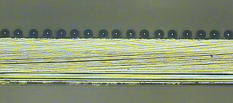
14 Bumped FE-I Chip IBM 0.25 µm rad tolerant design Chip with 9 column pairs Defect Classes Small Bump Large Bump Particle Bump Position Missing Bump
![IC Technology Roadmap: Chip Interconnect Pitch Chip Interconnect Pitch [µm]](/docs-images/90/102847784/images/15-0.jpg "180 160 140 120 100 80 60 40 20 0 ATLAS 2000 2005 2010 2015 2020 Year area")


15 IC Technology Roadmap: Chip Interconnect Pitch Chip Interconnect Pitch [µm] ATLAS Year area array peripheral Source: ITRS ATLAS Si-Sensor Substrate Wafer 520 Processed Sensor Wafer: 100 mm Silicon Wafer Double side processed Thickness 250 µm 3 sensor tiles with pixel cells 50 x 400(600) µm² Electroplated Sensor Pixel Contacts : Pixelmetallization Al Plating Base Ti:W/Cu Pad 5 µm Cu + 1µm Ni + Au


16 Bare Module Flip Chip Assembly readout chips, sensor tiles: test, inspection, classification flux deposition pick and place: FC150 of SüssMicrotech, Pick & Place Accuracy 3µm reflow: at 250 C, reductive atmosphere inspection and measurements: x-ray inspection, electric module test rework: single die exchange of misplaced die, to many bridged bumps, die that failed electrical test Assembly of ATLAS Pixel Detector Modules 16 ROC Flip-Chip Bonded to the Sensor electroplated SnPb IO-Bumps, Ø 25 µm, pitch 50 µm Assembly of 1139 ATLAS Modules Assembled Chips: ~ chips Module Yield incl. rework: 97 % Chip Rework Rate: 0.7 % Chip Yield after Bumping: processed Readout Chips 98% der Module mit <10 Bumpdefekten Class 1: perfect chips Class 2: accepted defects (< 4 defective bumps, small particle,...) Calss 3: rejected chips (> 4 defective bumps, scratches, residues, plating defects,...)


17 ATLAS Pixel Detector at LHC at CERN Bare Module 22 x 64 mm² PIXEL Detector Ø 0.9m ATLAS Detector Ø 25m Inner Detector Ø 2m ATLAS Pixel Detector at LHC at CERN


18 ATLAS Pixel Detector at LHC at CERN


19 Detector Placquettes for CMS 1 x 1 2 x 3 1 x 3

20 Future Requirements: Bump size and Pitch Solder Bumping PbSn37/63 Diameter: 10 µm Pitch: 20 µm Future Requirements: Lead Free Solder for Melting FC Interconnects Point SnBi 42/ C PbSn 37/ C SnZn 91/9 199 C SnAg 96.5/ C SnCu 99.3/ C AuSn 80/ C PbSn 95/5 314 C


21 Lead Free Bumping SnAg Meeting the requirements of future environmentally friendly lead-free flip chip interconnects basing on the EU-directive ROHS 2000 Bump dimensions Size: µm Pitch: down to 50 µm Ag composition: 3.0 ~ 4.0 at.% Melting point: 221 C Lead Free Bumping SnAg


22 GaAs X-ray Pixel Detector Frontend Readout Chip MEDIPIX 256x256 IOs Pixel cell size 55 x 55 µm² Chip size 14 x 14 mm² SnAg Bumps Ø25 µm, more than bumps/wafer GaAs Sensor Chip GaAs Detector 256x256 pixels Pixel size 55 x 55 µm² Chip size 16 x 16 mm² Electroplated Cu-Pad, height 5 µm project partners: MPD, Fine Tech, FhG-IZFP, FhG-IZM funded by: EFRE and the Free State of Saxony GaAs Hybrid Pixeldetector: X-Ray Test Pixeldetector assembled on MEDIPIX board and tested at FhG-IZFP x-ray images of a spring and a screw using the 202x202 pixel detector prototyp (photography by FhG-IZFP) project partners: MPD, Fine Tech, FhG-IZFP, FhG-IZM funded by: EFRE and the Free State of Saxony


23 AuSn Bumping for RF- Devices - AuSn Bumps on GaAs typ size diameter: 40 µm Hight: µm ζ-phase ep. Au sp. Au Ti:W(N) Chip Pad Pass. AuSn Electroplated Bumps 50 µm pitch full array 30 µm AuSn20 x-ray pixel detector


")


24 Cu Pillar Bumps (Height: 80 µm, Diameter: 60 µm) Process Flow - Stencil Printing Al bond pad Ni UBM Solder paste Cleaned solder bump Reflowed solder bump Source:


25 Electroless Ni + Solder Printing Solder Bumping by Stencil Printing 150 µm pitch 500 µm pitch Waferbumping by C4NP


26 Waferbumping by C4NP
 Solder with 3 or more components Fine Pitch")
27 Waferbumping by C4NP Waferbumping by C4NP Bumping of thinned wafers Bumping of wafers with vias (stacking) Solder with 3 or more components Fine Pitch Bumping


28 Elastic Contact Structures ELASTec Source: Infineon ClawConnect made of StressedMetall : J-shaped planar microspring Source: NanoNexus, Xerox Co., PARC Source: Georgia Tech Nano - structured Bump surface


29 Future Requirements: Integration of Passive Components Build up for the realization of all three passive types Thin Film Build Up for the Realization of Passives Future Requirements: Integration of Passive Components thinfilm resistors thinfilm inductors R = 1kΩ R = 5kΩ


30 Future Requirements: Thin Silicon Thinning of bumped wafers: 180 µm


 shorter process times")

31 Future Requirements: Thin Silicon Silicon becommes flexible when thickness is reduced down to less than 30µm bending radius 1mm / 1µm thickness fully flexible and ultra thin systems available best opportunities to proceed with FC and CSP technologies basis for 3D chip integration Dicing by Thinning Rounded chip corners Dry Etching of about 30µm deep groves Backside Grinding - Etching - CMP nearly ideal chip edges (rounded corners are possible) shorter process times for singulation into individual chips narrow cuts save silicon area for small chips non rectangular dies are possible non-rectangular dies

32 Wafer Level 3D Integration Technologies Stacking Technologies: Die-Stacking Pyramid Stack Same Size Stack with Spacer


33 Stacking Technologies: Die-Stacking Chip-in-Polymer Die-Stack Through Silicon Via Die-Stack Stacking Technologies: Wafer-Stacking Yield!!!

34 Through Silicon Vias: Basic Questions Pre Front End Process Post Front End Process New Front End Process Restrictions in Process Parameters Design Restrictions Through Silicon Vias: Basic Questions Wafer Front Side Processing - Wafer Back Side Processing


35 Wafer-Level-Packaging for Optical Applications Tapered Vias & Streets controlled sidewall angle for sribe line controlled sidewall angle for via holes Ball Grid Array on the backside with Silicon Via Contacts
 Side Wall Insulation Via Filling by Cu-CVD/ Via Filling by Cu-Electroplating Via Filling by W")
36 Wafer-Level-Packaging for Optical Applications Through Silicon Vias TSV Formation and Metallization Deep Via High Aspect Ratio Etching (h >20 µm 80 µm) Side Wall Insulation Via Filling by Cu-CVD/ Via Filling by Cu-Electroplating Via Filling by W - CVD


37 Through Silicon Vias: Si Etching Si Trench Etch 2.5 x 20 µm² How Deep is the Via? Through Silicon Vias: Via Filling W- Fill of High Aspect Ratio Trench ICV-Dimensions: 3 µm x 10 µm x 50 µm 300 nm SACVD TEOS 20 nm TiN CVD 900 nm W CVD und W Backetch 800 nm M1 (AlSiCu, structured) 850 nm PN/POX (Passiviation)


38 Through Silicon Vias: Via Filling Deep Inter-Chip Vias AR 20:1 W-Fill and Etch Back 23,4 µm W (via-fill) SACVD Oxide Through Silicon Vias: Via Filling Copper CVD

39

 Opening")


40 Process flow Fabrication of inter-chip vias with standard wafer process sequence Simultaneous formation of electrical and mechanical connection Fabrication of Tungsten or Copper filled InterChip Vias on Top Substrate Via Opening and Metallization Thinning (20µm) Opening of Plugs Electroplating CMOS Top Wafer prior to Thinning 10x2,5 µm ICVs TEOS M2-AlSiCu SACVD planarized ILD TEOS Therm. Oxide O3/TEOS Spacer MOCVD-TiN/W ICVs 10 x 2,5 µm, 20 µm deep, AR 8:1 Distance between W-filled ICVs and Transistors: ~ 4 µm to Source/Drain Area ~ 11 µm to Gate Area


41 Process flow Simultaneous formation of electrical and mechanical connection Alignment and Soldering to the Bottom Wafer
 Dept. High Density Interconnect & Wafer Level Packaging Gustav-Meyer-Allee 25, 13355 Berlin Tel.")
42 Process flow Alignment and Soldering of additional Top Chips - Thin SLID layers with large area contacts - Modular concept - Suitable for chip-to-wafer stacking Integration densities up to 10 5 cm -2 Fraunhofer Institut Zuverlässigkeit und Mikrointegration (IZM) Dept. High Density Interconnect & Wafer Level Packaging Gustav-Meyer-Allee 25, Berlin Tel.: +49 (0) , Fax: -123 Forschungsschwerpunkt Technologien der Mikroperipherik, TIB Sekr. 4/2-1 Gustav-Meyer-Allee 25, Berlin Tel.: +49 (0) , Fax:
Fraunhofer IZM - ASSID
 FRAUNHOFER-INSTITUT FÜR Zuverlässigkeit und Mikrointegration IZM Fraunhofer IZM - ASSID All Silicon System Integration Dresden Heterogeneous 3D Wafer Level System Integration 3D system integration is one
50 Micron Pitch Flip Chip Bumping Technology: Processes and Applications
 50 Micron Pitch Flip Chip Bumping Technology: Processes and Applications Alan Huffman Center for Materials and Electronic Technologies huffman@rti.org Outline RTI Identity/History Historical development
Electroless Bumping for 300mm Wafers
 Electroless Bumping for 300mm Wafers T. Oppert Internepcon 2006 Tokyo Big Sight, Japan Outline Short Company Profile Electroless Ni/Au Under Bump Metallization UBM for Copper Devices Solder Bumping: Stencil
B. Flip-Chip Technology
 B. Flip-Chip Technology B1. Level 1. Introduction to Flip-Chip techniques B1.1 Why flip-chip? In the development of packaging of electronics the aim is to lower cost, increase the packaging density, improve
SOLDER BUMP FLIP CHIP BONDING FOR PIXEL DETECTOR HYBRIDIZATION
 SOLDER BUMP FLIP CHIP BONDING FOR PIXEL DETECTOR HYBRIDIZATION Jorma Salmi and Jaakko Salonen VTT Information Technology Microelectronics P.O. Box 1208 FIN-02044 VTT, Finland (visiting: Micronova, Tietotie
Electronic Packaging Technologies from Bump Bonding to 3D Integration
 Electronic Packaging Technologies from Bump Bonding to 3D Integration Fraunhofer Institute for Reliability and Microintegration (IZM) Gustav-Meyer-Allee 25 13355 Berlin Germany Dipl.-Ing. Thomas Fritzsch
Hermetic Packaging Solutions using Borosilicate Glass Thin Films. Lithoglas Hermetic Packaging Solutions using Borosilicate Glass Thin Films
 Hermetic Packaging Solutions using Borosilicate Glass Thin Films 1 Company Profile Company founded in 2006 ISO 9001:2008 qualified since 2011 Headquarters and Production in Dresden, Germany Production
CMP for More Than Moore
 2009 Levitronix Conference on CMP Gerfried Zwicker Fraunhofer Institute for Silicon Technology ISIT Itzehoe, Germany gerfried.zwicker@isit.fraunhofer.de Contents Moore s Law and More Than Moore Comparison:
(a) (d) (e) (b) (c) (f) 3D-NAND Flash and Its Manufacturing Process
 (d) (e) (b) (c) (f) 3D-NAND Flash and Its Manufacturing Process") 3D-NAND Flash and Its Manufacturing Process 79 (d) Si Si (b) (c) (e) Si (f) +1-2 (g) (h) Figure 2.33 Top-down view in cap oxide and (b) in nitride_n-2; (c) cross-section near the top of the channel; top-down
3D-NAND Flash and Its Manufacturing Process 79 (d) Si Si (b) (c) (e) Si (f) +1-2 (g) (h) Figure 2.33 Top-down view in cap oxide and (b) in nitride_n-2; (c) cross-section near the top of the channel; top-down
Fabrication of a High-Density MCM-D for a Pixel Detector System using a BCB/Cu Technology
 Fabrication of a High-Density MCM-D for a Pixel Detector System using a BCB/Cu Technology M. Töpper, L. Dietrich, G. Engelmann, S. Fehlberg, P. Gerlach*, J. Wolf, O. Ehrmann, K.-H. Becks*, H. Reichl Technical
Drucktechnik für das moderne Packaging - Teil 2
 Drucktechnik für das moderne Packaging - Teil 2 Dipl.-Ing. Technical University of Berlin (TUB) Gustav-Meyer-Allee 25, 13355 Berlin, Germany email: coskina@izm.fhg.de Fraunhofer Institute for Reliability
Laser Solder Attach for Optoelectronics Packages
 1 Laser Solder Attach for Optoelectronics Packages Elke Zakel, Lars Titerle, Thomas Oppert, Ronald G. Blankenhorn* Pac Tech Packaging Technologies GmbH Am Schlangenhorst 15-17, Germany Phone:+ 49 (0) 33
Pixeldetector Modules in Multi Chip Module - Deposited Technology
 Pixeldetector Modules in Multi Chip Module - Deposited Technology Tobias Flick (K.-H. Becks, P. Gerlach, Ch. Grah, P.Mättig) University of Wuppertal 8th Topical Seminar on Innovative Particle and Radiation
Flip Chip Bumping & Assembly
 6. Europäisches Elektroniktechnologie-Kolleg 19.-23. März 2003 Colonia de Sant Jordi, Mallorca - Club Colonia Sant Jordi Flip Chip Bumping & Assembly Hermann Oppermann Fraunhofer IZM, Berlin Gustav-Meyer-Allee
IMAGE SENSOR EVOLUTION AND ENABLING 3D TECHNOLOGIES
 Fig. 5: Scanning Electron Microscopy images (TOP view, 3D view, Zoome including all metal levels of the BSI imager structure. (dashed line shows bonding IMAGE SENSOR EVOLUTION AND ENABLING 3D TECHNOLOGIES
Introduction of IMS Technology for Advanced Solder Bumping on Wafers / Laminates
 Introduction of IMS Technology for Advanced Solder Bumping on Wafers / Laminates Science & Technology IBM Research Tokyo Yasumitsu Orii, PhD Senju Metal Industry Co.,TW Deputy General Manager Lewis Huang
The Role of Flip Chip Bonding in Advanced Packaging David Pedder
 The Role of Flip Chip Bonding in Advanced Packaging David Pedder David Pedder Associates Stanford in the Vale Faringdon Oxfordshire The Role of Flip Chip Bonding in Advanced Packaging Outline Flip Chip
64 Channel Flip-Chip Mounted Selectively Oxidized GaAs VCSEL Array
 64 Channel Flip-Chip Mounted Selectively Oxidized GaAs VCSEL Array 69 64 Channel Flip-Chip Mounted Selectively Oxidized GaAs VCSEL Array Roland Jäger and Christian Jung We have designed and fabricated
A Low-cost Through Via Interconnection for ISM WLP
 A Low-cost Through Via Interconnection for ISM WLP Jingli Yuan, Won-Kyu Jeung, Chang-Hyun Lim, Seung-Wook Park, Young-Do Kweon, Sung Yi To cite this version: Jingli Yuan, Won-Kyu Jeung, Chang-Hyun Lim,
SAMPLE SLIDES & COURSE OUTLINE. Core Competency In Semiconductor Technology: 2. FABRICATION. Dr. Theodore (Ted) Dellin
 Dellin") & Digging Deeper Devices, Fabrication & Reliability For More Info:.com or email Dellin@ieee.org SAMPLE SLIDES & COURSE OUTLINE In : 2. A Easy, Effective, of How Devices Are.. Recommended for everyone who
& Digging Deeper Devices, Fabrication & Reliability For More Info:.com or email Dellin@ieee.org SAMPLE SLIDES & COURSE OUTLINE In : 2. A Easy, Effective, of How Devices Are.. Recommended for everyone who
Application Note AN-1011
 AN-1011 Board Mounting Application Note for 0.800mm Pitch Devices For part numbers IRF6100, IRF6100PBF, IR130CSP, IR130CSPPBF, IR140CSP, IR140CSPPBF, IR1H40CSP, IR1H40CSPPBF By Hazel Schofield and Philip
Chemnitzer Seminar System Integration Technologies. Solder Jetting, Rework & electroless UBM Deposition
 Chemnitzer Seminar System Integration Technologies June 14 15, 2016 Solder Jetting, Rework & electroless UBM Deposition Made in Germany PacTech Group - Milestones 1995 PacTech founded in Berlin, Germany
Assembly/Packagng RF-PCB. Thick Film. Thin Film. Screening/Test. Design Manual
 Thick Film Thin Film RF-PCB Assembly/Packagng Screening/Test Design Manual RHe Design Manual The following rules are effective for the draft of circuit boards and hybrid assemblies. The instructions are
Integration of 3D detector systems
 Integration of 3D detector systems Piet De Moor Introduction Evolution in radiation detection/imaging: single pixel linear array 2D array increase in resolution = decrease in pitch (down to few um) = thanks
Processes for Flexible Electronic Systems
 Processes for Flexible Electronic Systems Michael Feil Fraunhofer Institut feil@izm-m.fraunhofer.de Outline Introduction Single sheet versus reel-to-reel (R2R) Substrate materials R2R printing processes
Fabrication of a High-Density MCM-D for a Pixel Detector System using a BCB/Cu/PbSn Technology
 Fabrication of a High-Density MCM-D for a Pixel Detector System using a BCB/Cu/PbSn Technology M. Töpper, P. Gerlach*, L. Dietrich, S. Fehlberg, C. Karduck, C. Meinherz, J. Wolf, O. Ehrmann, K.-H. Becks*,
Lecture: Integration of silicon photonics with electronics. Prepared by Jean-Marc FEDELI CEA-LETI
 Lecture: Integration of silicon photonics with electronics Prepared by Jean-Marc FEDELI CEA-LETI Context The goal is to give optical functionalities to electronics integrated circuit (EIC) The objectives
NEW PACKAGING AND INTERCONNECT TECHNOLOGIES FOR ULTRA THIN CHIPS
 NEW PACKAGING AND INTERCONNECT TECHNOLOGIES FOR ULTRA THIN CHIPS Christine Kallmayer and Rolf Aschenbrenner Fraunhofer IZM Berlin, Germany kallmayer@izm.fhg.de Julian Haberland and Herbert Reichl Technical
Studies on MCM D interconnections
 Studies on MCM D interconnections Speaker: Peter Gerlach Department of Physics Bergische Universität Wuppertal D-42097 Wuppertal, GERMANY Authors: K.H.Becks, T.Flick, P.Gerlach, C.Grah, P.Mättig Department
"Low Cost Electroless Bumping for Ultra Fine Pitch Applications in 8" and 12" Wafers"
 1 "Low Cost Electroless Bumping for Ultra Fine Pitch Applications in 8" and 12" Wafers" Elke Zakel, Thomas Oppert, Ghassem Azdasht, Thorsten Teutsch * Pac Tech Packaging Technologies GmbH Am Schlangenhorst
Getting the FLI Lead Out. Thomas J. De Bonis Assembly & Test Technology Development Technology and Manufacturing Group
 Getting the FLI Lead Out Thomas J. De Bonis Assembly & Test Technology Development Technology and Manufacturing Group Lead has been used in flip chip FLI for decades. RoHS Exemption 15 was enacted in recognition
An Introduction to Electronics Systems Packaging. Prof. G. V. Mahesh. Department of Electronic Systems Engineering
 An Introduction to Electronics Systems Packaging Prof. G. V. Mahesh Department of Electronic Systems Engineering India Institute of Science, Bangalore Module No. # 02 Lecture No. # 08 Wafer Packaging Packaging
Application Note 5026
 Surface Laminar Circuit (SLC) Ball Grid Array (BGA) Eutectic Surface Mount Assembly Application Note 5026 Introduction This document outlines the design and assembly guidelines for surface laminar circuitry
EMERGING SUBSTRATE TECHNOLOGIES FOR PACKAGING
 EMERGING SUBSTRATE TECHNOLOGIES FOR PACKAGING Henry H. Utsunomiya Interconnection Technologies, Inc. Suwa City, Nagano Prefecture, Japan henryutsunomiya@mac.com ABSTRACT This presentation will outline
Powerchip Semiconductor Corporation A3R12E3GEF G6E 635BLC4M 512 Megabit DDR2 SDRAM Structural Analysis
 February 23, 2007 Powerchip Semiconductor Corporation A3R12E3GEF G6E 635BLC4M Structural Analysis For comments, questions, or more information about this report, or for any additional technical needs concerning
The Compact Muon Solenoid Experiment. Conference Report. Mailing address: CMS CERN, CH-1211 GENEVA 23, Switzerland
 Available on CMS information server CMS CR -2015/280 The Compact Muon Solenoid Experiment Conference Report Mailing address: CMS CERN, CH-1211 GENEVA 23, Switzerland 02 November 2015 (v2, 06 November 2015)
POSSUM TM Die Design as a Low Cost 3D Packaging Alternative
 POSSUM TM Die Design as a Low Cost 3D Packaging Alternative The trend toward 3D system integration in a small form factor has accelerated even more with the introduction of smartphones and tablets. Integration
450mm and Moore s Law Advanced Packaging Challenges and the Impact of 3D
 450mm and Moore s Law Advanced Packaging Challenges and the Impact of 3D Doug Anberg VP, Technical Marketing Ultratech SOKUDO Lithography Breakfast Forum July 10, 2013 Agenda Next Generation Technology
Advanced High-Density Interconnection Technology
 Advanced High-Density Interconnection Technology Osamu Nakao 1 This report introduces Fujikura s all-polyimide IVH (interstitial Via Hole)-multi-layer circuit boards and device-embedding technology. Employing
Flip chip Assembly with Sub-micron 3D Re-alignment via Solder Surface Tension
 Flip chip Assembly with Sub-micron 3D Re-alignment via Solder Surface Tension Jae-Woong Nah*, Yves Martin, Swetha Kamlapurkar, Sebastian Engelmann, Robert L. Bruce, and Tymon Barwicz IBM T. J. Watson Research
Benzocyclobutene Polymer dielectric from Dow Chemical used for wafer-level redistribution.
 Glossary of Advanced Packaging: ACA Bare Die BCB BGA BLT BT C4 CBGA CCC CCGA CDIP or CerDIP CLCC COB COF CPGA Anisotropic Conductive Adhesive Adhesive with conducting filler particles where the electrical
Brief Introduction of Sigurd IC package Assembly
 Brief Introduction of Sigurd IC package Assembly Content Package Development Trend Product Brief Sawing type QFN Representative MEMS Product LGA Light Sensor Proximity Sensor High Yield Capability Low
!"#$"%&' ()#*+,-+.&/0(
#*+,-+.&/0(") !"#$"%&' ()#*+,-+.&/0( Multi Chip Modules (MCM) or Multi chip packaging Industry s first MCM from IBM. Generally MCMs are horizontal or two-dimensional modules. Defined as a single unit containing two
!"#$"%&' ()#*+,-+.&/0( Multi Chip Modules (MCM) or Multi chip packaging Industry s first MCM from IBM. Generally MCMs are horizontal or two-dimensional modules. Defined as a single unit containing two
nvidia GeForce FX 5700 Ultra (NV36) Graphics Processor Structural Analysis
 Graphics Processor Structural Analysis") nvidia GeForce FX 5700 Ultra (NV36) Graphics Processor Structural Analysis For questions, comments, or more information about this report, or for any additional technical needs concerning semiconductor
nvidia GeForce FX 5700 Ultra (NV36) Graphics Processor Structural Analysis For questions, comments, or more information about this report, or for any additional technical needs concerning semiconductor
Product Catalog. Semiconductor Intellectual Property & Technology Licensing Program
 Product Catalog Semiconductor Intellectual Property & Technology Licensing Program MANUFACTURING PROCESS TECHNOLOGY OVERVIEW 90 nm 130 nm 0.18 µm 0.25 µm 0.35 µm >0.40 µm Logic CMOS SOI CMOS SOI CMOS SOI
Advanced Packaging Equipment Solder Jetting & Laser Bonding
 Advanced Packaging Equipment Solder Jetting & Laser Bonding www.pactech.comw.pactech.com PacTech Packaging Technologies Pioneering in laser solder jetting technologies since 1995 Our mission is to reshape
Chapter 2. Literature Review
 Chapter 2 Literature Review 2.1 Development of Electronic Packaging Electronic Packaging is to assemble an integrated circuit device with specific function and to connect with other electronic devices.
Sony IMX Megapixel, 1.4 µm Pixel 1/3.2 Optical Format CMOS Image Sensor
 Sony IMX046 8.11 Megapixel, 1.4 µm Pixel 1/3.2 Optical Format CMOS Image Sensor Imager Process Review For comments, questions, or more information about this report, or for any additional technical needs
UMS User guide for bare dies GaAs MMIC. storage, pick & place, die attach and wire bonding
 UMS User guide for bare dies GaAs MMIC storage, pick & place, die attach and wire bonding Ref. : AN00014097-07 Apr 14 1/10 Specifications subject to change without notice United Monolithic Semiconductors
Through Glass Via (TGV) Technology for RF Applications
 Technology for RF Applications") Through Glass Via (TGV) Technology for RF Applications C. H. Yun 1, S. Kuramochi 2, and A. B. Shorey 3 1 Qualcomm Technologies, Inc. 5775 Morehouse Dr., San Diego, California 92121, USA Ph: +1-858-651-5449,
Through Glass Via (TGV) Technology for RF Applications C. H. Yun 1, S. Kuramochi 2, and A. B. Shorey 3 1 Qualcomm Technologies, Inc. 5775 Morehouse Dr., San Diego, California 92121, USA Ph: +1-858-651-5449,
Nanotechnology, the infrastructure, and IBM s research projects
 Nanotechnology, the infrastructure, and IBM s research projects Dr. Paul Seidler Coordinator Nanotechnology Center, IBM Research - Zurich Nanotechnology is the understanding and control of matter at dimensions
IWORID J. Schmitz page 1. Wafer-level CMOS post-processing Jurriaan Schmitz
 IWORID J. Schmitz page 1 Wafer-level CMOS post-processing Jurriaan Schmitz IWORID J. Schmitz page 2 Outline Introduction on wafer-level post-proc. CMOS: a smart, but fragile substrate Post-processing steps
Fabricating 2.5D, 3D, 5.5D Devices
 Fabricating 2.5D, 3D, 5.5D Devices Bob Patti, CTO rpatti@tezzaron.com Tezzar on Semiconduct or 04/15/2013 1 Gen4 Dis-Integrated 3D Memory DRAM layers 42nm node 2 million vertical connections per lay per
Flip-Chip for MM-Wave and Broadband Packaging
 1 Flip-Chip for MM-Wave and Broadband Packaging Wolfgang Heinrich Ferdinand-Braun-Institut für Höchstfrequenztechnik (FBH) Berlin / Germany with contributions by F. J. Schmückle Motivation Growing markets
Chapter 3 Basics Semiconductor Devices and Processing
 Chapter 3 Basics Semiconductor Devices and Processing 1 Objectives Identify at least two semiconductor materials from the periodic table of elements List n-type and p-type dopants Describe a diode and
TAIPRO Engineering. Speaker: M. Saint-Mard Managing director. TAIlored microsystem improving your PROduct
 TAIPRO Engineering MEMS packaging is crucial for system performance and reliability Speaker: M. Saint-Mard Managing director TAIPRO ENGINEERING SA Michel Saint-Mard Administrateur délégué m.saintmard@taipro.be
Endoscopic Inspection of Area Array Packages
 Endoscopic Inspection of Area Array Packages Meeting Miniaturization Requirements For Defect Detection BY MARCO KAEMPFERT Area array packages such as the family of ball grid array (BGA) components plastic
Two major features of this text
 Two major features of this text Since explanatory materials are systematically made based on subject examination questions, preparation
Laser Assisted Flip Chip Assembly for LCD Applications using ACP and NCP Adhesive Joining
 1 Laser Assisted Flip Chip Assembly for LCD Applications using ACP and NCP Adhesive Joining Elke Zakel, Ghassem Azdasht, Thorsten Teutsch *, Ronald G. Blankenhorn* Pac Tech Packaging Technologies GmbH
High Efficient Heat Dissipation on Printed Circuit Boards. Markus Wille, R&D Manager, Schoeller Electronics Systems GmbH
 High Efficient Heat Dissipation on Printed Circuit Boards Markus Wille, R&D Manager, Schoeller Electronics Systems GmbH m.wille@se-pcb.de Introduction 2 Heat Flux: Q x y Q z The substrate (insulation)
Advances in X-Ray Technology for Semicon Applications Keith Bryant and Thorsten Rother
 Advances in X-Ray Technology for Semicon Applications Keith Bryant and Thorsten Rother X-Ray Champions, Telspec, Yxlon International Agenda The x-ray tube, the heart of the system Advances in digital detectors
3D ICs: Recent Advances in the Industry
 3D ICs: Recent Advances in the Industry Suresh Ramalingam Senior Director, Advanced Packaging Outline 3D IC Background 3D IC Technology Development Summary Acknowledgements Stacked Silicon Interconnect
CHAPTER 11: Testing, Assembly, and Packaging
 Chapter 11 1 CHAPTER 11: Testing, Assembly, and Packaging The previous chapters focus on the fabrication of devices in silicon or the frontend technology. Hundreds of chips can be built on a single wafer,
Process Certification and Defect Recognition: Hybrids, Microcircuits and RF/MMIC Modules (3 DAYS)
") Process Certification and Defect Recognition: Hybrids, Microcircuits and RF/MMIC Modules (3 DAYS) Course Description: Most companies struggle to introduce new lines and waste countless manhours and resources
Process Certification and Defect Recognition: Hybrids, Microcircuits and RF/MMIC Modules (3 DAYS) Course Description: Most companies struggle to introduce new lines and waste countless manhours and resources
23. Packaging of Electronic Equipments (2)
") 23. Packaging of Electronic Equipments (2) 23.1 Packaging and Interconnection Techniques Introduction Electronic packaging, which for many years was only an afterthought in the design and manufacture of
23. Packaging of Electronic Equipments (2) 23.1 Packaging and Interconnection Techniques Introduction Electronic packaging, which for many years was only an afterthought in the design and manufacture of
Packaging Roadmap: The impact of miniaturization. Bob Pfahl, inemi Celestica-iNEMI Technology Forum May 15, 2007
 Packaging Roadmap: The impact of miniaturization Bob Pfahl, inemi Celestica-iNEMI Technology Forum May 15, 2007 The Challenges for the Next Decade Addressing the consumer experience using the converged
Microsoft X02046 IBM PowerPC Processor from the XBOX 360 Structural Analysis
 February 7, 2006 Microsoft X02046 IBM PowerPC Processor from the XBOX 360 Structural Analysis For comments, questions, or more information about this report, or for any additional technical needs concerning
Winter College on Optics: Fundamentals of Photonics - Theory, Devices and Applications February 2014
 2572-10 Winter College on Optics: Fundamentals of Photonics - Theory, Devices and Applications 10-21 February 2014 Photonic packaging and integration technologies II Sonia M. García Blanco University of
Chapter 3: Basics Semiconductor Devices and Processing 2006/9/27 1. Topics
 Chapter 3: Basics Semiconductor Devices and Processing 2006/9/27 1 Topics What is semiconductor Basic semiconductor devices Basics of IC processing CMOS technologies 2006/9/27 2 1 What is Semiconductor
MICROELECTRONICS ASSSEMBLY TECHNOLOGIES. The QFN Platform as a Chip Packaging Foundation
 West Coast Luncheon January 15, 2014. PROMEX PROMEX INDUSTRIES INC. MICROELECTRONICS ASSSEMBLY TECHNOLOGIES The QFN Platform as a Chip Packaging Foundation 3075 Oakmead Village Drive Santa Clara CA Ɩ 95051
MID Manufacturing Process.
 3D Aerosol Jet Printing An Emerging MID Manufacturing Process. Dr. Martin Hedges Neotech Services MTP, Nuremberg, Germany info@neotechservices.com Aerosol Jet Printing Aerosol Jet Process Overview Current
Tape Automated Bonding
 Tape Automated Bonding Introduction TAB evolved from the minimod project begun at General Electric in 1965, and the term Tape Automated Bonding was coined by Gerard Dehaine of Honeywell Bull in 1971. The
Intel Xeon E3-1230V2 CPU Ivy Bridge Tri-Gate 22 nm Process
 Intel Xeon E3-1230V2 CPU Structural Analysis 3685 Richmond Road, Suite 500, Ottawa, ON K2H 5B7 Canada Tel: 613-829-0414 www.chipworks.com Structural Analysis Some of the information in this report may
Trends in Advanced Packaging Technologies An IMAPS UK view
 Trends in Advanced Packaging Technologies An IMAPS UK view Andy Longford Chair IMAPS UK 2007 9 PandA Europe IMAPS UK IeMRC Interconnection event December 2008 1 International Microelectronics And Packaging
3D TSV Micro Cu Column Chip-to-Substrate/Chip Assmbly/Packaging Technology
 3D TSV Micro Cu Column Chip-to-Substrate/Chip Assmbly/Packaging Technology by Seung Wook Yoon, *K. T. Kang, W. K. Choi, * H. T. Lee, Andy C. B. Yong and Pandi C. Marimuthu STATS ChipPAC LTD, 5 Yishun Street
Silicon Detectors in High Energy Physics
 Thomas Bergauer (HEPHY Vienna) IPM Teheran 22 May 2011 Sunday: Schedule Semiconductor Basics (45 ) Silicon Detectors in Detector concepts: Pixels and Strips (45 ) Coffee Break Strip Detector Performance
BGA (Ball Grid Array)
") BGA (Ball Grid Array) National Semiconductor Application Note 1126 November 2002 Table of Contents Introduction... 2 Package Overview... 3 PBGA (PLASTIC BGA) CONSTRUCTION... 3 TE-PBGA (THERMALLY ENHANCED
BGA (Ball Grid Array) National Semiconductor Application Note 1126 November 2002 Table of Contents Introduction... 2 Package Overview... 3 PBGA (PLASTIC BGA) CONSTRUCTION... 3 TE-PBGA (THERMALLY ENHANCED
Jan Bogaerts imec
 imec 2007 1 Radiometric Performance Enhancement of APS 3 rd Microelectronic Presentation Days, Estec, March 7-8, 2007 Outline Introduction Backside illuminated APS detector Approach CMOS APS (readout)
Bob Willis Process Guides
 What is a Printed Circuit Board Pad? What is a printed circuit board pad, it may sound like a dumb question but do you stop to think what it really does and how its size is defined and why? A printed circuit
Plan Optik AG. Plan Optik AG PRODUCT CATALOGUE
 Plan Optik AG Plan Optik AG PRODUCT CATALOGUE 2 In order to service the high demand of wafers more quickly, Plan Optik provides off the shelf products in sizes from 2 up to 300mm diameter. Therefore Plan
Strip Detectors. Principal: Silicon strip detector. Ingrid--MariaGregor,SemiconductorsasParticleDetectors. metallization (Al) p +--strips
 p +--strips") Strip Detectors First detector devices using the lithographic capabilities of microelectronics First Silicon detectors -- > strip detectors Can be found in all high energy physics experiments of the last
Strip Detectors First detector devices using the lithographic capabilities of microelectronics First Silicon detectors -- > strip detectors Can be found in all high energy physics experiments of the last
3D devices for the ILC
 3D devices for the ILC Our work on 3D integrated circuits began when we considered challenges of an ILC vertex detector in 2006 High resolution small pixels Low mass thinned sensors and electronics Time
EE 330 Lecture 11. Capacitances in Interconnects Back-end Processing
 EE 330 Lecture 11 Capacitances in Interconnects Back-end Processing Exam 1 Friday Sept 21 Students may bring 1 page of notes HW assignment for week of Sept 16 due on Wed Sept 19 at beginning of class No
BGA/CSP Re-balling Bob Doetzer Circuit Technology Inc.
 BGA/CSP Re-balling Bob Doetzer Circuit Technology Inc. www.circuittechnology.com The trend in the electronics interconnect industry towards Area Array Packages type packages (BGA s, CSP s, CGA s etc.)
Chapter 11 Testing, Assembly, and Packaging
 Chapter 11 Testing, Assembly, and Packaging Professor Paul K. Chu Testing The finished wafer is put on a holder and aligned for testing under a microscope Each chip on the wafer is inspected by a multiple-point
Silicon Interposers enable high performance capacitors
 Interposers between ICs and package substrates that contain thin film capacitors have been used previously in order to improve circuit performance. However, with the interconnect inductance due to wire
Mobile Electrostatic Carrier (MEC) evaluation for a GaAs wafer backside manufacturing process
 evaluation for a GaAs wafer backside manufacturing process") Mobile Electrostatic Carrier (MEC) evaluation for a GaAs wafer backside manufacturing process H.Stieglauer 1, J.Nösser 1, A.Miller 1, M.Lanz 1, D.Öttlin 1, G.Jonsson 1, D.Behammer 1, C.Landesberger 2,
Mobile Electrostatic Carrier (MEC) evaluation for a GaAs wafer backside manufacturing process H.Stieglauer 1, J.Nösser 1, A.Miller 1, M.Lanz 1, D.Öttlin 1, G.Jonsson 1, D.Behammer 1, C.Landesberger 2,
Aptina MT9P111 5 Megapixel, 1/4 Inch Optical Format, System-on-Chip (SoC) CMOS Image Sensor
 CMOS Image Sensor") Aptina MT9P111 5 Megapixel, 1/4 Inch Optical Format, System-on-Chip (SoC) CMOS Image Sensor Imager Process Review For comments, questions, or more information about this report, or for any additional technical
Aptina MT9P111 5 Megapixel, 1/4 Inch Optical Format, System-on-Chip (SoC) CMOS Image Sensor Imager Process Review For comments, questions, or more information about this report, or for any additional technical
Sectional Design Standard for High Density Interconnect (HDI) Printed Boards
 Printed Boards") IPC-2226 ASSOCIATION CONNECTING ELECTRONICS INDUSTRIES Sectional Design Standard for High Density Interconnect (HDI) Printed Boards Developed by the HDI Design Subcommittee (D-41) of the HDI Committee
IPC-2226 ASSOCIATION CONNECTING ELECTRONICS INDUSTRIES Sectional Design Standard for High Density Interconnect (HDI) Printed Boards Developed by the HDI Design Subcommittee (D-41) of the HDI Committee
WLCSP and FlipChip Production Bumping Using Electroless Ni/Au Plating And Wafer Level Solder Sphere Transfer Technologies
 WLCSP and FlipChip Production Bumping Using Electroless Ni/Au Plating And Wafer Level Solder Sphere Transfer Technologies Andrew Strandjord, Jing Li, Axel Scheffler, and Thorsten Teutsch PacTech - Packaging
Chapter 3 Fabrication
 Chapter 3 Fabrication The total structure of MO pick-up contains four parts: 1. A sub-micro aperture underneath the SIL The sub-micro aperture is used to limit the final spot size from 300nm to 600nm for
Data Sheet _ R&D. Rev Date: 8/17
 Data Sheet _ R&D Rev Date: 8/17 Micro Bump In coming years the interconnect density for several applications such as micro display, imaging devices will approach the pitch 10um and below. Many research
Preparing for the Future: Upgrades of the CMS Pixel Detector
 : KSETA Plenary Workshop, Durbach, KIT Die Forschungsuniversität in der Helmholtz-Gemeinschaft www.kit.edu Large Hadron Collider at CERN Since 2015: proton proton collisions @ 13 TeV Four experiments:
To See is to Survive!
 INSPECTION SYSTEMS for the 21 s t Century To See is to Survive! In todayõs highly competitive manufacturing environment, the ability to see and react to hidden production deficiencies, in order to guarantee
Application Bulletin 240
 Application Bulletin 240 Design Consideration CUSTOM CAPABILITIES Standard PC board fabrication flexibility allows for various component orientations, mounting features, and interconnect schemes. The starting
Semiconductor Process Diagnosis and Prognosis for DSfM
 Semiconductor Process Diagnosis and Prognosis for DSfM Department of Electronic Engineering Prof. Sang Jeen Hong Nov. 19, 2014 1/2 Agenda 1. Semiconductor Manufacturing Industry 2. Roles of Semiconductor
Samsung S5K3BAFB 2 Megapixel CMOS Image Sensor 0.13 µm Copper CMOS Process Process Review Report
 October 13, 2006 Samsung S5K3BAFB 2 Megapixel CMOS Image Sensor 0.13 µm Copper CMOS Process Process Review Report (with Optional TEM Analysis) For comments, questions, or more information about this report,
The Problems. Spheretek Wafer Bumping The Low Cost and Reliable Solution to Production Wafer Packaging
 Spheretek Wafer Bumping The Low Cost and Reliable Solution to Production Wafer Packaging The Problems. Packaging Production engineers and their CFO s have to date been disappointed in the results of their
REVISION #25, 12/12/2012
 HYPRES NIOBIUM INTEGRATED CIRCUIT FABRICATION PROCESS #03-10-45 DESIGN RULES REVISION #25, 12/12/2012 Direct all inquiries, questions, comments and suggestions concerning these design rules and/or HYPRES
Min Tao, Ph. D, Ashok Prabhu, Akash Agrawal, Ilyas Mohammed, Ph. D, Bel Haba, Ph. D Oct , IWLPC
 PACKAGE-ON-PACKAGE INTERCONNECT FOR FAN-OUT WAFER LEVEL PACKAGES Min Tao, Ph. D, Ashok Prabhu, Akash Agrawal, Ilyas Mohammed, Ph. D, Bel Haba, Ph. D Oct 18-20 2016, IWLPC 1 Outline Laminate to Fan-Out