50 Micron Pitch Flip Chip Bumping Technology: Processes and Applications
|
|
|
- Horace Phelps
- 6 years ago
- Views:
Transcription

1 50 Micron Pitch Flip Chip Bumping Technology: Processes and Applications Alan Huffman Center for Materials and Electronic Technologies Outline RTI Identity/History Historical development of solder bumping at RTI Fine Pitch Solder Bump Technology Fine Pitch Bumping Processes Post Bump Processes Hybridization Applications What kinds of devices need fine pitch? Compact Muon Solenoid (CMS) MEDIPIX Future directions of fine pitch interconnects 3D integration technology Alternative bump materials VISA-like structures 1
2 Who We Are Since 1958, our mission has defined us Private, Independent, 501(c)(3), non-profit Recognized as the physical and intellectual cornerstone of the Research Triangle Park. One of the largest non-profit R&D organizations in the US RTI International at a Glance 2500 employees half with advanced degrees multidisciplinary FY05 revenues of $467.7M Broad array of clients Select Clients Government clients: DOD DOE NASA EPA USAID DHHS Commercial clients: Eastman Gasification Services Süd Chemie Air Liquide BOC Chevron-Texaco General Electric 2

3 RTI International Practice Areas Defense Homeland Security Education and Training Health and Pharmaceuticals Energy, Environment, and Natural Resources International Development Advanced Technology Who We Used To Be The acquisition of MCNC-RDI was completed in March 2005 RTI International to Acquire Three Divisions of MCNC s Research and Development Institute RESEARCH TRIANGLE PARK, N.C. (Sept. 15, 2004) As part of a strategy to strengthen its core research and development capabilities, RTI International today announced that it intends to acquire three research divisions of MCNC s Research and Development Institute (MCNCRDI) later this year. The research divisions being acquired include MCNC s Signal Electronics Division, Materials and Electronic Technologies Division and Advanced Network Research Division. MCNC s Grid Computing and Ventures business units are not included in the RTI acquisition. 3
 Shadow mask manually aligned to the wafer to define pad and bump location Minimum bump pitch ~ 225 µm Typical bump height 100-125 µm Expensive high end applications A")
4 A Brief History of Flip Chip Development at RTI 1965: IBM introduces Controlled Collapse Chip Connection (C4) process Evaporated high-lead solder bumps onto an evaporated Cr/Cr-Cu/Cu/Au thin-film under bump metallurgy (UBM) Shadow mask manually aligned to the wafer to define pad and bump location Minimum bump pitch ~ 225 µm Typical bump height µm Expensive high end applications A Brief History of Flip Chip Development at RTI UBM Evaporation High Lead Bump Evaporation Reflow 4


5 A Brief History of Flip Chip Development at RTI In the early 1990 s researchers at MCNC develop electroplated solder deposition processes to replace evaporation Patterned photoresist replaces shadow mask as the bump deposition template Alignment between wafer features and bumps is improved through photolithography Minimum bump size and pitch is now theoretically not limited 90/10 97/3 Pb/Sn solder bump composition UBM structure is still based on IBM Cr/Cr-Cu/Cu Awarded DARPA contract to further develop this technology for commercial and government use, created the Flip Chip Technology Center Electroplated Bump Process Flow Incoming Wafer With I/O Pads Plate Solder Repassivation Strip Resist Template UBM Deposition Reflow Apply and Define Plating Template Etch Field UBM 5
6 A Brief History of Flip Chip Development at RTI Mid-1990 s: Several changes to base bumping process are made Shift from high lead solder to eutectic Sn/Pb Reduction of MP from high lead to eutectic reduces thermal stress on devices Lower reflow temperature (183 C vs. 312 C) allows a shift from ceramic substrates to organic laminate substrates Shift from evaporated to sputtered UBM Less complicated structure, fewer metal layers Suitable for high Sn solders Adoption of BCB as repassivation material Extremely low moisture absorption Lower cure temperature than PI Lower dielectric constant A Brief History of Flip Chip Development at RTI 1997: MCNC enters the Seamless High Off- Chip Connectivity (SHOCC) Consortium DARPA program aimed at developing technologies to shift design paradigms from single die approaches to a parallel manufacturing approach utilizing yield-optimized IC elements connected to a common substrate Required the development of sub-100 µm pitch area array solder bumps to interconnect ICs on the substrate 1998: MCNC spins off Unitive Electronics as a for-profit commercial bumping company MCNC continues fine pitch bumping technology as the basis for its advanced packaging research, proof of concept, and prototyping activities 6
7 A Brief History of Flip Chip Development at RTI March 2005: RTI acquires the research divisions of MCNC-RDI to add additional research capabilities and directions to the Science & Engineering Group Present Day: RTI continues to support prototype, proof of concept, and small volume production for emerging and niche applications and research into new areas of advanced packaging and interconnect Fine Pitch Bumping Processes 7
8 Fine Pitch Solder Bumping Formation of fine pitch solder bumps uses essentially the same processes as standard flip chip Repassivation UBM Deposition Bumping template application Solder Electroplating UBM Etching Bump Reflow The main difference is the degree of process control must be high and the margins for error are low Repassivation BCB (Dow Chemical) is applied to the wafer surface Allows for a consistent base material for the bumping process, regardless of the surface of the incoming wafer Provides a stress buffer under the solder bumps Provides protection to the wafer through subsequent process steps Planarizes the wafer surface, evening out topographical differences Vias are photolithographically opened over device I/O pads Must have high degree of control over photolithography process due to BCB process limits 8

9 Repassivation BCB Inorganic Dielectric Silicon Aluminum Pad Dicing Street Repassivation 9

10 Repassivation UBM Deposition Sputtered thin film metal UBM system Provides excellent contact resistance and adhesion to both BCB surface and I/O metal Structure is engineered to provide good current carrying characteristics for uniform electroplating, but must be thin enough to mitigate undercut during UBM etch UBM BCB Inorganic Dielectric Silicon Aluminum Pad Dicing Street 10
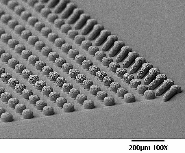
11 Bumping Template Application Typically a thick spin-on photoresist, some require multiple coats New dry-film photoresists (DuPont) for wafer level packaging applications Alignment of bump template to I/O is critical and more difficult for fine pitch designs Alignment tolerances reduced from +/- 5 µm for typical WLP to +/- 1-2 µm for fine pitch 1X exposure tools make this more difficult Complete development of the template openings is more difficult due to their size Bumping Template Application 11


12 Bumping Template Application 25 µm 125 µm Comparison of typical flip chip bump template opening to fine pitch Bumping Template Application 12
 Ni/Au pads are used as solder wettable joining pads on mating parts for Sn/Pb")
13 Bumping Template Application Dry film photoresist bumping template Solder Electroplating Electroplating is the only practical deposition technology for fine pitch bumping Any bump material can be used, so long as it is compatible with the UBM and template material and can be electroplated (Sn/Pb, Pb-free, Au, etc) Ni/Au pads are used as solder wettable joining pads on mating parts for Sn/Pb bumps Wafer level uniformity for fine pitch designs is achieved through Multiple cathode contact points around the perimeter of the wafer An good current-carrying plane (UBM) Plating cell design, solution flow dynamics Changes to the plating current profile: DC pulse plating 13

14 Electroplating Electroplating 14
15 UBM Etch Removal of field UBM metal to electrically isolate the bumps Typically achieved through chemical etching, but some metals are removed through dry etching/plasma processes Control of bump undercut is extremely important for fine pitch designs 250 µm base diameter with 2 µm undercut on each side 246 µm effective base diameter, 1.6% loss 25 µm base diameter with 2 µm undercut on each side 21 µm effective base diameter, 16% loss Loss of bump base contact area = reduced bump strength Reflow Bumps are melted in an inert atmosphere with a reducing agent (usually flux) to form the familiar spherical shape Flux residues are removed from the wafer after reflow with solvents 15

16 Reflow Post-Bumping Wafer Thinning Wafer thinning is done after bumping to prevent excessive handling and processing of thin wafers A protective coating is applied to the wafer to protect the bumps during the taping, thinning, and de-taping processes Wafer thinning process consists of two steps Grind: to quickly remove Si from the wafer backside Stress relief: to remove the damaged Si layer and alleviate the stress created in the silicon during the grind Protective layer is removed prior to dicing 16
 on some")

17 Dicing Considerations Thinned wafers are more susceptible to chipping damage during dicing and require different blades and parameters Dicing kerf must be very close to the active area (50 µm or less) on some devices to allow close placement in multi-chip module assembly Thin, high resistivity silicon sensor wafers are susceptible to chipping and microcracking during dicing, which increases the leakage current Poorly Diced Sensor Wafers 17


18 ROC Dicing Cleanly Diced Sensor 18
19 Assembly High throughput flip chip assembly tools usually do not have the placement accuracy to reliably place fine pitch bumped devices Need <5 µm placement accuracy MCM assemblies usually have neighboring die edges placed <150 µm apart Chip placement process must not disturb previously placed devices Flux is undesirable in the assembly process Difficult to remove flux residues from under large chips with very small standoff gap Post-Assembly Chip Standoff Gap 70 Gap between chip and substrate Bump pitch (micron) 19

 treatment time Leaves no")
20 Standard Vs. Fine-Pitch Assembly 250 µm Pitch 50 µm Pitch 250um Pitch 50um Pitch Chip-to-substrate gap reduces from 65µm to 22µm for 25µm diameter bumps Plasma Assisted Dry Soldering (PADS) Replaces flux in assembly process Solder-bearing parts treated prior to assembly Short (10-15 min) treatment time Leaves no residues on chip or substrate Proven applications in SMT, MEMS, photonics, flip chip packaging Patented 20
21 Who Needs Fine Pitch Bumping? ITRS Roadmap For Bump Pitch BGA Ball Pitch Hand Held 0.65 mm 0.65 mm 0.65 mm 0.5 mm 0.5 mm 0.5 mm CSP Bump Pitch 0.3 mm 0.2 mm 0.2 mm 0.15 mm 0.15 mm 0.1 mm Flip Chip Bump Pitch 130 µm 120 µm 100 µm 90 µm 80 µm 70 µm From: ITRS 2004 Update 21
22 Devices That Require Fine Pitch Bumping Pixelated Detector Arrays High energy physics particle detectors X-Ray imaging detectors Smart Pixel Arrays Optoelectronic element arrays of VCELS, photodetectors MEMS High Performance I/C s & Processors 3D Integrated Electronics Focal plane arrays Characteristics of Fine Pitch Devices High interconnect counts, from a few thousand to over 65,000 Large chip size (~ 1 cm 2 and larger) Many are pixelated devices for imaging and detection Small pixel size gives higher resolution to image Mating devices are typically both made of silicon, thus reducing CTE reliability issues Wirebond terminals and bumps are commonly needed on the same device 22

23 The Compact Muon Solenoid (CMS) High energy physics particle detector being built at CERN in Switzerland for the Large Hadron Collider (LHC) Goals of CMS Explore physics at the TeV scale Find the Higgs boson, the subatomic particle in the Standard Model theorized to regulate mass Study heavy ion collisions RTI is building part of one of the particle detectors that will be at the core of the system by bump bonding readout chips and sensor devices together into MCMs of different sizes The CMS System 23

24 CMS Detector Modules Readout chips are fabricated on full thickness 8-inch silicon wafers and are thinned to 200 µm prior to assembly, 4160 bumps per chip Sensor wafers are fabricated on 350 µm thick high resistivity wafers Bump size is 25 micron base diameter with a minimum I/O pitch of 50 microns 6 different module sizes: 1x1, 1x2, 1x5, 2x3, 2x4, 2x5 Full detector will require over 800 total modules with about 5000 individual readout chips Total number of bumped connections is over 19,000,000 Solder Bumped CMS ROC 24

 25")
25 Solder Bumped CMS ROC Solder Bumped ROC and Sensor (US-CMS) 25


26 Pixilated Detector Module Assemblies CMS single and multi-chip sensor modules CMS Detector Module Assemblies 2x4 detector module in test fixture Courtesy: US-CMS FPix Collaboration 26
27 CMS Yield Data Recent evaluation of CMS FPix detector modules (61 total modules, 1,626,560 bump connections) Bump bonding yield of 99.66% 60 of 61 modules meet leakage current specifications at 250V 59 of 61 modules meet leakage current specifications at 600V Power consumption on all modules within spec Courtesy: US-CMS FPix Collaboration MEDIPIX Consortium - CERN X-ray/gamma ray detector devices working in single photon counting mode 55 µm pitch, uniform in both directions Detector modules of 1x1 (~1 in 2 ) and 2x2 (~4 in 2 ) MEDIPIX ASIC is used in conjunction with different sensor devices for a number of applications X-ray imaging Biological radiography Neutron detection 27
 50 µm")


28 Solder Bumped ROC and Sensor (MEDIPIX) 50 µm pitch readout chip with eutectic Sn/Pb bumps 50 µm pitch sensor chip with Ni/Au bump bond pads MEDIPIX Detector Module 28
29 Future Hybridization Technologies 3D Integration Alternative Bump Materials Alternative Singulation Processes 3D Integration Through via interconnects (TVI) are formed through bulk silicon in active devices Allows multiple device layers to be interconnected front-to-back TVIs can be formed before or after devices are physically joined together Significant process differences between vias-first process and vias-last process Process used dictated by device design and process compatibility Allows array sizes that are not limited to 1xN or 2xN modules: true area array ROC placement 29


30 Benefits of 3D Integration: Pixelated Devices 3-D Integration allows massively parallel signal processing Dramatically increased electronic functionality in each pixel Detector/Sensor Arrays Actuator Arrays 3-D Interconnects Mirror MEMS Actuator Spatial light modulators w/digital control of optical wave front phases 3-D ROIC 3-D Interconnects 3-D Sensor Arrays Large formats with high resolution On-chip signal processing Reduction of size, weight & power DARPA Coherent Communications, Imaging & Targeting (CCIT) program 3-D Actuator Arrays Large formats with high resolution Low switching energy & latency Reduction of size, weight & power Test Structure Operability Test 256x256 ROIC 25 µm 20 µm 65,536 interconnects in ~1 cm 2 Operability Map Si IC Die # % Operable Insulator Copper 14 Defective pixels Si IC Nonfunctional cell Demonstrated 99.98% operability in 256x256 arrays with 4 µm vias on 30 µm pitch 30


31 Alternative Bump Materials Non-collapsible bump materials may be useful for extremely small bump interconnections (~5 µm dia.) Sn-capped Cu bumps Alternatives to Saw Dicing Silicon etching using Bosch process allows damage-free singulation of ROCsand sensor devices Dicing streets must be free of metal Deposit and pattern photoresist Bosch etching complete Bosch etching Photoresist removal 31
32 Conclusion RTI has developed the processes for fine pitch bumping and assembly and supports prototype, small volume, and leading edge applications A growing infrastructure to support back end processes such as dicing and grinding is in place While large volume applications for fine pitch flip chip bumping do not exist yet, there are special applications which are using this technology today Fin Alan Huffman huffman@rti.org
SOLDER BUMP FLIP CHIP BONDING FOR PIXEL DETECTOR HYBRIDIZATION
 SOLDER BUMP FLIP CHIP BONDING FOR PIXEL DETECTOR HYBRIDIZATION Jorma Salmi and Jaakko Salonen VTT Information Technology Microelectronics P.O. Box 1208 FIN-02044 VTT, Finland (visiting: Micronova, Tietotie
Application Note 5026
 Surface Laminar Circuit (SLC) Ball Grid Array (BGA) Eutectic Surface Mount Assembly Application Note 5026 Introduction This document outlines the design and assembly guidelines for surface laminar circuitry
Hermetic Packaging Solutions using Borosilicate Glass Thin Films. Lithoglas Hermetic Packaging Solutions using Borosilicate Glass Thin Films
 Hermetic Packaging Solutions using Borosilicate Glass Thin Films 1 Company Profile Company founded in 2006 ISO 9001:2008 qualified since 2011 Headquarters and Production in Dresden, Germany Production
IMAGE SENSOR EVOLUTION AND ENABLING 3D TECHNOLOGIES
 Fig. 5: Scanning Electron Microscopy images (TOP view, 3D view, Zoome including all metal levels of the BSI imager structure. (dashed line shows bonding IMAGE SENSOR EVOLUTION AND ENABLING 3D TECHNOLOGIES
B. Flip-Chip Technology
 B. Flip-Chip Technology B1. Level 1. Introduction to Flip-Chip techniques B1.1 Why flip-chip? In the development of packaging of electronics the aim is to lower cost, increase the packaging density, improve
Application Note AN-1011
 AN-1011 Board Mounting Application Note for 0.800mm Pitch Devices For part numbers IRF6100, IRF6100PBF, IR130CSP, IR130CSPPBF, IR140CSP, IR140CSPPBF, IR1H40CSP, IR1H40CSPPBF By Hazel Schofield and Philip
64 Channel Flip-Chip Mounted Selectively Oxidized GaAs VCSEL Array
 64 Channel Flip-Chip Mounted Selectively Oxidized GaAs VCSEL Array 69 64 Channel Flip-Chip Mounted Selectively Oxidized GaAs VCSEL Array Roland Jäger and Christian Jung We have designed and fabricated
Electroless Bumping for 300mm Wafers
 Electroless Bumping for 300mm Wafers T. Oppert Internepcon 2006 Tokyo Big Sight, Japan Outline Short Company Profile Electroless Ni/Au Under Bump Metallization UBM for Copper Devices Solder Bumping: Stencil
Introduction of IMS Technology for Advanced Solder Bumping on Wafers / Laminates
 Introduction of IMS Technology for Advanced Solder Bumping on Wafers / Laminates Science & Technology IBM Research Tokyo Yasumitsu Orii, PhD Senju Metal Industry Co.,TW Deputy General Manager Lewis Huang
Processes for Flexible Electronic Systems
 Processes for Flexible Electronic Systems Michael Feil Fraunhofer Institut feil@izm-m.fraunhofer.de Outline Introduction Single sheet versus reel-to-reel (R2R) Substrate materials R2R printing processes
POSSUM TM Die Design as a Low Cost 3D Packaging Alternative
 POSSUM TM Die Design as a Low Cost 3D Packaging Alternative The trend toward 3D system integration in a small form factor has accelerated even more with the introduction of smartphones and tablets. Integration
BGA/CSP Re-balling Bob Doetzer Circuit Technology Inc.
 BGA/CSP Re-balling Bob Doetzer Circuit Technology Inc. www.circuittechnology.com The trend in the electronics interconnect industry towards Area Array Packages type packages (BGA s, CSP s, CGA s etc.)
An Introduction to Electronics Systems Packaging. Prof. G. V. Mahesh. Department of Electronic Systems Engineering
 An Introduction to Electronics Systems Packaging Prof. G. V. Mahesh Department of Electronic Systems Engineering India Institute of Science, Bangalore Module No. # 02 Lecture No. # 08 Wafer Packaging Packaging
Laser Solder Attach for Optoelectronics Packages
 1 Laser Solder Attach for Optoelectronics Packages Elke Zakel, Lars Titerle, Thomas Oppert, Ronald G. Blankenhorn* Pac Tech Packaging Technologies GmbH Am Schlangenhorst 15-17, Germany Phone:+ 49 (0) 33
The Role of Flip Chip Bonding in Advanced Packaging David Pedder
 The Role of Flip Chip Bonding in Advanced Packaging David Pedder David Pedder Associates Stanford in the Vale Faringdon Oxfordshire The Role of Flip Chip Bonding in Advanced Packaging Outline Flip Chip
The Compact Muon Solenoid Experiment. Conference Report. Mailing address: CMS CERN, CH-1211 GENEVA 23, Switzerland
 Available on CMS information server CMS CR -2015/280 The Compact Muon Solenoid Experiment Conference Report Mailing address: CMS CERN, CH-1211 GENEVA 23, Switzerland 02 November 2015 (v2, 06 November 2015)
Advanced Packaging - Pulsed-laser Heating for Flip Chip Assembly
 Page 1 of 5 Pulsed-laser Heating for Flip Chip Assembly A stress-free alternative By Thorsten Teutsch, Ph.D., Pac Tech USA, Elke Zakel, Ph.D., and Ghassem Azdasht, Pac Tech GmbH As flip chip applications
Wafer Level System Integration. Oswin Ehrmann
 Wafer Level System Integration Oswin Ehrmann Fraunhofer Institut for Reliability and Microintegration IZM D-13355 Berlin Germany Gustav-Meyer-Allee 25 Outline Introduction Wafer Bumping and Flip Chip Bonding
Flip chip Assembly with Sub-micron 3D Re-alignment via Solder Surface Tension
 Flip chip Assembly with Sub-micron 3D Re-alignment via Solder Surface Tension Jae-Woong Nah*, Yves Martin, Swetha Kamlapurkar, Sebastian Engelmann, Robert L. Bruce, and Tymon Barwicz IBM T. J. Watson Research
Fraunhofer IZM - ASSID
 FRAUNHOFER-INSTITUT FÜR Zuverlässigkeit und Mikrointegration IZM Fraunhofer IZM - ASSID All Silicon System Integration Dresden Heterogeneous 3D Wafer Level System Integration 3D system integration is one
The Problems. Spheretek Wafer Bumping The Low Cost and Reliable Solution to Production Wafer Packaging
 Spheretek Wafer Bumping The Low Cost and Reliable Solution to Production Wafer Packaging The Problems. Packaging Production engineers and their CFO s have to date been disappointed in the results of their
Flip Chips. FA10-200x200 FA10-400x400 FA10-600x x 200 mils 400 x 400 mils
 Flip Chip FlipChip International Flip Chip describes the method of electrically connecting the die to the package carrier. The package carrier, either substrate or leadframe, then provides the connection
Application Bulletin 240
 Application Bulletin 240 Design Consideration CUSTOM CAPABILITIES Standard PC board fabrication flexibility allows for various component orientations, mounting features, and interconnect schemes. The starting
A Technique for Improving the Yields of Fine Feature Prints
 A Technique for Improving the Yields of Fine Feature Prints Dr. Gerald Pham-Van-Diep and Frank Andres Cookson Electronics Equipment 16 Forge Park Franklin, MA 02038 Abstract A technique that enhances the
Flexline - A Flexible Manufacturing Method for Wafer Level Packages (Extended Abstract)
") Flexline - A Flexible Manufacturing Method for Wafer Level Packages (Extended Abstract) by Tom Strothmann, *Damien Pricolo, **Seung Wook Yoon, **Yaojian Lin STATS ChipPAC Inc.1711 W Greentree Drive Tempe,
Flexline - A Flexible Manufacturing Method for Wafer Level Packages (Extended Abstract) by Tom Strothmann, *Damien Pricolo, **Seung Wook Yoon, **Yaojian Lin STATS ChipPAC Inc.1711 W Greentree Drive Tempe,
Assembly Instructions for SCA6x0 and SCA10x0 series
 Technical Note 71 Assembly Instructions for SCA6x0 and SCA10x0 series TABLE OF CONTENTS Table of Contents...1 1 Objective...2 2 VTI'S DIL-8 and DIL-12 packages...2 3 Package Outline and Dimensions...2
SAMPLE SLIDES & COURSE OUTLINE. Core Competency In Semiconductor Technology: 2. FABRICATION. Dr. Theodore (Ted) Dellin
 Dellin") & Digging Deeper Devices, Fabrication & Reliability For More Info:.com or email Dellin@ieee.org SAMPLE SLIDES & COURSE OUTLINE In : 2. A Easy, Effective, of How Devices Are.. Recommended for everyone who
& Digging Deeper Devices, Fabrication & Reliability For More Info:.com or email Dellin@ieee.org SAMPLE SLIDES & COURSE OUTLINE In : 2. A Easy, Effective, of How Devices Are.. Recommended for everyone who
Assembly Instructions for SCC1XX0 series
 Technical Note 82 Assembly Instructions for SCC1XX0 series TABLE OF CONTENTS Table of Contents...1 1 Objective...2 2 VTI's 32-lead Dual In-line Package (DIL-32)...2 3 DIL-32 Package Outline and Dimensions...2
MICROBUMP CREATION SYSTEM FOR ADVANCED PACKAGING APPLICATIONS
 MICROBUMP CREATION SYSTEM FOR ADVANCED PACKAGING APPLICATIONS Andrew Ahr, EKC Technology, & Chester E. Balut, DuPont Electronic Technologies Alan Huffman, RTI International Abstract Today, the electronics
A Low-cost Through Via Interconnection for ISM WLP
 A Low-cost Through Via Interconnection for ISM WLP Jingli Yuan, Won-Kyu Jeung, Chang-Hyun Lim, Seung-Wook Park, Young-Do Kweon, Sung Yi To cite this version: Jingli Yuan, Won-Kyu Jeung, Chang-Hyun Lim,
Chemnitzer Seminar System Integration Technologies. Solder Jetting, Rework & electroless UBM Deposition
 Chemnitzer Seminar System Integration Technologies June 14 15, 2016 Solder Jetting, Rework & electroless UBM Deposition Made in Germany PacTech Group - Milestones 1995 PacTech founded in Berlin, Germany
Lithography in our Connected World
 Lithography in our Connected World SEMI Austin Spring Forum TOP PAN P R INTING CO., LTD MATER IAL SOLUTIONS DIVISION Toppan Printing Co., LTD A Broad-Based Global Printing Company Foundation: January 17,
Chapter 11 Testing, Assembly, and Packaging
 Chapter 11 Testing, Assembly, and Packaging Professor Paul K. Chu Testing The finished wafer is put on a holder and aligned for testing under a microscope Each chip on the wafer is inspected by a multiple-point
3D TSV Micro Cu Column Chip-to-Substrate/Chip Assmbly/Packaging Technology
 3D TSV Micro Cu Column Chip-to-Substrate/Chip Assmbly/Packaging Technology by Seung Wook Yoon, *K. T. Kang, W. K. Choi, * H. T. Lee, Andy C. B. Yong and Pandi C. Marimuthu STATS ChipPAC LTD, 5 Yishun Street
Advanced Packaging Equipment Solder Jetting & Laser Bonding
 Advanced Packaging Equipment Solder Jetting & Laser Bonding www.pactech.comw.pactech.com PacTech Packaging Technologies Pioneering in laser solder jetting technologies since 1995 Our mission is to reshape
Lecture 7. Lithography and Pattern Transfer. Reading: Chapter 7
 Lecture 7 Lithography and Pattern Transfer Reading: Chapter 7 Used for Pattern transfer into oxides, metals, semiconductors. 3 types of Photoresists (PR): Lithography and Photoresists 1.) Positive: PR
Min Tao, Ph. D, Ashok Prabhu, Akash Agrawal, Ilyas Mohammed, Ph. D, Bel Haba, Ph. D Oct , IWLPC
 PACKAGE-ON-PACKAGE INTERCONNECT FOR FAN-OUT WAFER LEVEL PACKAGES Min Tao, Ph. D, Ashok Prabhu, Akash Agrawal, Ilyas Mohammed, Ph. D, Bel Haba, Ph. D Oct 18-20 2016, IWLPC 1 Outline Laminate to Fan-Out
Flip-Chip for MM-Wave and Broadband Packaging
 1 Flip-Chip for MM-Wave and Broadband Packaging Wolfgang Heinrich Ferdinand-Braun-Institut für Höchstfrequenztechnik (FBH) Berlin / Germany with contributions by F. J. Schmückle Motivation Growing markets
Bob Willis Process Guides
 What is a Printed Circuit Board Pad? What is a printed circuit board pad, it may sound like a dumb question but do you stop to think what it really does and how its size is defined and why? A printed circuit
IWORID J. Schmitz page 1. Wafer-level CMOS post-processing Jurriaan Schmitz
 IWORID J. Schmitz page 1 Wafer-level CMOS post-processing Jurriaan Schmitz IWORID J. Schmitz page 2 Outline Introduction on wafer-level post-proc. CMOS: a smart, but fragile substrate Post-processing steps
Studies on MCM D interconnections
 Studies on MCM D interconnections Speaker: Peter Gerlach Department of Physics Bergische Universität Wuppertal D-42097 Wuppertal, GERMANY Authors: K.H.Becks, T.Flick, P.Gerlach, C.Grah, P.Mättig Department
Getting the FLI Lead Out. Thomas J. De Bonis Assembly & Test Technology Development Technology and Manufacturing Group
 Getting the FLI Lead Out Thomas J. De Bonis Assembly & Test Technology Development Technology and Manufacturing Group Lead has been used in flip chip FLI for decades. RoHS Exemption 15 was enacted in recognition
Data Sheet _ R&D. Rev Date: 8/17
 Data Sheet _ R&D Rev Date: 8/17 Micro Bump In coming years the interconnect density for several applications such as micro display, imaging devices will approach the pitch 10um and below. Many research
Figure 7 Dynamic range expansion of Shack- Hartmann sensor using a spatial-light modulator
 Figure 4 Advantage of having smaller focal spot on CCD with super-fine pixels: Larger focal point compromises the sensitivity, spatial resolution, and accuracy. Figure 1 Typical microlens array for Shack-Hartmann
Two major features of this text
 Two major features of this text Since explanatory materials are systematically made based on subject examination questions, preparation
CHAPTER 11: Testing, Assembly, and Packaging
 Chapter 11 1 CHAPTER 11: Testing, Assembly, and Packaging The previous chapters focus on the fabrication of devices in silicon or the frontend technology. Hundreds of chips can be built on a single wafer,
Benzocyclobutene Polymer dielectric from Dow Chemical used for wafer-level redistribution.
 Glossary of Advanced Packaging: ACA Bare Die BCB BGA BLT BT C4 CBGA CCC CCGA CDIP or CerDIP CLCC COB COF CPGA Anisotropic Conductive Adhesive Adhesive with conducting filler particles where the electrical
Laser Assisted Flip Chip Assembly for LCD Applications using ACP and NCP Adhesive Joining
 1 Laser Assisted Flip Chip Assembly for LCD Applications using ACP and NCP Adhesive Joining Elke Zakel, Ghassem Azdasht, Thorsten Teutsch *, Ronald G. Blankenhorn* Pac Tech Packaging Technologies GmbH
Production of HPDs for the LHCb RICH Detectors
 Production of HPDs for the LHCb RICH Detectors LHCb RICH Detectors Hybrid Photon Detector Production Photo Detector Test Facilities Test Results Conclusions IEEE Nuclear Science Symposium Wyndham, 24 th
Pixeldetector Modules in Multi Chip Module - Deposited Technology
 Pixeldetector Modules in Multi Chip Module - Deposited Technology Tobias Flick (K.-H. Becks, P. Gerlach, Ch. Grah, P.Mättig) University of Wuppertal 8th Topical Seminar on Innovative Particle and Radiation
Advances in stacked-die packaging
 pg.10-15-carson-art 16/6/03 4:12 pm Page 1 The stacking of die within IC packages, primarily Chip Scale Packages (CSP) Ball Grid Arrays (BGAs) has evolved rapidly over the last few years. The now standard
Advanced High-Density Interconnection Technology
 Advanced High-Density Interconnection Technology Osamu Nakao 1 This report introduces Fujikura s all-polyimide IVH (interstitial Via Hole)-multi-layer circuit boards and device-embedding technology. Employing
"Low Cost Electroless Bumping for Ultra Fine Pitch Applications in 8" and 12" Wafers"
 1 "Low Cost Electroless Bumping for Ultra Fine Pitch Applications in 8" and 12" Wafers" Elke Zakel, Thomas Oppert, Ghassem Azdasht, Thorsten Teutsch * Pac Tech Packaging Technologies GmbH Am Schlangenhorst
EMERGING SUBSTRATE TECHNOLOGIES FOR PACKAGING
 EMERGING SUBSTRATE TECHNOLOGIES FOR PACKAGING Henry H. Utsunomiya Interconnection Technologies, Inc. Suwa City, Nagano Prefecture, Japan henryutsunomiya@mac.com ABSTRACT This presentation will outline
Technology for the MEMS processing and testing environment. SUSS MicroTec AG Dr. Hans-Georg Kapitza
 Technology for the MEMS processing and testing environment SUSS MicroTec AG Dr. Hans-Georg Kapitza 1 SUSS MicroTec Industrial Group Founded 1949 as Karl Süss KG GmbH&Co. in Garching/ Munich San Jose Waterbury
PAGE 1/6 ISSUE SERIES Micro-SPDT PART NUMBER R516 XXX 10X. (All dimensions are in mm [inches]) R 516 _ 1 0 _
![PAGE 1/6 ISSUE SERIES Micro-SPDT PART NUMBER R516 XXX 10X. (All dimensions are in mm [inches]) R 516 _ 1 0 _](/thumbs/96/127769340.jpg "PAGE 1/6 ISSUE SERIES Micro-SPDT PART NUMBER R516 XXX 10X. (All dimensions are in mm [inches]) R 516 _ 1 0 _") PAGE 1/6 ISSUE 15-10-18 SERIES Micro-SPDT PART NUMBER R516 XXX 10X R516 series: the RAMSES concept merges with the SLIM LINE technology, breaking up the frequency limits of SMT switches : - FULL SMT TECHNOLOGY
PAGE 1/6 ISSUE 15-10-18 SERIES Micro-SPDT PART NUMBER R516 XXX 10X R516 series: the RAMSES concept merges with the SLIM LINE technology, breaking up the frequency limits of SMT switches : - FULL SMT TECHNOLOGY
Lecture: Integration of silicon photonics with electronics. Prepared by Jean-Marc FEDELI CEA-LETI
 Lecture: Integration of silicon photonics with electronics Prepared by Jean-Marc FEDELI CEA-LETI Context The goal is to give optical functionalities to electronics integrated circuit (EIC) The objectives
PAGE 1/6 ISSUE Jul SERIES Micro-SPDT PART NUMBER R516 XXX 10X R 516 _ 1 0 _
 PAGE 1/6 ISSUE Jul-24-2017 SERIES Micro-SPDT PART NUMBER R516 XXX 10X R516 series: the RAMSES concept merges with the SLIM LINE technology, breaking up the frequency limits of SMT switches : - FULL SMT
Fabrication of a High-Density MCM-D for a Pixel Detector System using a BCB/Cu Technology
 Fabrication of a High-Density MCM-D for a Pixel Detector System using a BCB/Cu Technology M. Töpper, L. Dietrich, G. Engelmann, S. Fehlberg, P. Gerlach*, J. Wolf, O. Ehrmann, K.-H. Becks*, H. Reichl Technical
Integration of 3D detector systems
 Integration of 3D detector systems Piet De Moor Introduction Evolution in radiation detection/imaging: single pixel linear array 2D array increase in resolution = decrease in pitch (down to few um) = thanks
Major Fabrication Steps in MOS Process Flow
 Major Fabrication Steps in MOS Process Flow UV light Mask oxygen Silicon dioxide photoresist exposed photoresist oxide Silicon substrate Oxidation (Field oxide) Photoresist Coating Mask-Wafer Alignment
The Future of Packaging ~ Advanced System Integration
 The Future of Packaging ~ Advanced System Integration Enabling a Microelectronic World R. Huemoeller SVP, Adv. Product / Platform Develop June 2013 Product Segments End Market % Share Summary 2 New Product
WLP User's Guide. CMOS IC Application Note. Rev.1.0_03. ABLIC Inc., 2014
 CMOS IC Application Note WLP User's Guide ABLIC Inc., 2014 This document is a reference manual that describes the handling of the mounting of super-small WLP (Wafer Level Package) for users in the semiconductor
Part 5-1: Lithography
 Part 5-1: Lithography Yao-Joe Yang 1 Pattern Transfer (Patterning) Types of lithography systems: Optical X-ray electron beam writer (non-traditional, no masks) Two-dimensional pattern transfer: limited
Silicon Interposers enable high performance capacitors
 Interposers between ICs and package substrates that contain thin film capacitors have been used previously in order to improve circuit performance. However, with the interconnect inductance due to wire
FLIP CHIP LED SOLDER ASSEMBLY
 As originally published in the SMTA Proceedings FLIP CHIP LED SOLDER ASSEMBLY Gyan Dutt, Srinath Himanshu, Nicholas Herrick, Amit Patel and Ranjit Pandher, Ph.D. Alpha Assembly Solutions South Plainfield,
User s Guide to. Centre for Materials for Electronics Technology Panchawati, Off Pashan Road, Pune September Version 2.
 User s Guide to Centre for Materials for Electronics Technology Panchawati, Off Pashan Road, Pune 411008 September 2013 Version 2.1 Contents 1 Designing of LTCC Structures and Design Rules... 01 1.1 Guidelines
Bumping of Silicon Wafers using Enclosed Printhead
 Bumping of Silicon Wafers using Enclosed Printhead By James H. Adriance Universal Instruments Corp. SMT Laboratory By Mark A. Whitmore DEK Screen Printers Advanced Technologies Introduction The technology
AN5046 Application note
 Application note Printed circuit board assembly recommendations for STMicroelectronics PowerFLAT packages Introduction The PowerFLAT package (5x6) was created to allow a larger die to fit in a standard
SESUB - Its Leadership In Embedded Die Packaging Technology
 SESUB - Its Leadership In Embedded Die Packaging Technology Sip Conference China 2018 TDK Corporation ECBC, PAF, SESUB BU Kofu, Japan October 17, 2018 Contents SESUB Introduction SESUB Process SESUB Quality
Flexible Hybrid Electronics Fabricated with High-Performance COTS ICs using RTI CircuitFilm TM Technology
 Flexible Hybrid Electronics Fabricated with High-Performance COTS ICs using RTI CircuitFilm TM Technology Scott Goodwin 1, Erik Vick 2 and Dorota Temple 2 1 Micross Advanced Interconnect Technology Micross
MICROELECTRONICS ASSSEMBLY TECHNOLOGIES. The QFN Platform as a Chip Packaging Foundation
 West Coast Luncheon January 15, 2014. PROMEX PROMEX INDUSTRIES INC. MICROELECTRONICS ASSSEMBLY TECHNOLOGIES The QFN Platform as a Chip Packaging Foundation 3075 Oakmead Village Drive Santa Clara CA Ɩ 95051
Diverse Lasers Support Key Microelectronic Packaging Tasks
 Diverse Lasers Support Key Microelectronic Packaging Tasks Written by D Muller, R Patzel, G Oulundsen, H Halou, E Rea 23 July 2018 To support more sophisticated and compact tablets, phones, watches and
Low Thermal Resistance Flip-Chip Bonding of 850nm 2-D VCSEL Arrays Capable of 10 Gbit/s/ch Operation
 Low Thermal Resistance Flip-Chip Bonding of 85nm -D VCSEL Arrays Capable of 1 Gbit/s/ch Operation Hendrik Roscher In 3, our well established technology of flip-chip mounted -D 85 nm backside-emitting VCSEL
Applications of Maskless Lithography for the Production of Large Area Substrates Using the SF-100 ELITE. Jay Sasserath, PhD
 Applications of Maskless Lithography for the Production of Large Area Substrates Using the SF-100 ELITE Executive Summary Jay Sasserath, PhD Intelligent Micro Patterning LLC St. Petersburg, Florida Processing
2 Integrated Circuit Manufacturing:
 2 Integrated Circuit Manufacturing: A Technology Resource 2 IC MANUFACTURING TECHNOLOGIES While the integrated circuit drives the packaging and assembly, the IC manufacturing process, and associated methodologies,
Innovations Push Package-on-Package Into New Markets. Flynn Carson. STATS ChipPAC Inc Kato Rd Fremont, CA 94538
 Innovations Push Package-on-Package Into New Markets by Flynn Carson STATS ChipPAC Inc. 47400 Kato Rd Fremont, CA 94538 Copyright 2010. Reprinted from Semiconductor International, April 2010. By choosing
WLCSP and FlipChip Production Bumping Using Electroless Ni/Au Plating And Wafer Level Solder Sphere Transfer Technologies
 WLCSP and FlipChip Production Bumping Using Electroless Ni/Au Plating And Wafer Level Solder Sphere Transfer Technologies Andrew Strandjord, Jing Li, Axel Scheffler, and Thorsten Teutsch PacTech - Packaging
Laminate Based Fan-Out Embedded Die Technologies: The Other Option
 Laminate Based Fan-Out Embedded Die Technologies: The Other Option Theodore (Ted) G. Tessier, Tanja Karila*, Tuomas Waris*, Mark Dhaenens and David Clark FlipChip International, LLC 3701 E University Drive
HOTBAR REFLOW SOLDERING
 HOTBAR REFLOW SOLDERING Content 1. Hotbar Reflow Soldering Introduction 2. Application Types 3. Process Descriptions > Flex to PCB > Wire to PCB 4. Design Guidelines 5. Equipment 6. Troubleshooting Guide
Through Glass Via (TGV) Technology for RF Applications
 Technology for RF Applications") Through Glass Via (TGV) Technology for RF Applications C. H. Yun 1, S. Kuramochi 2, and A. B. Shorey 3 1 Qualcomm Technologies, Inc. 5775 Morehouse Dr., San Diego, California 92121, USA Ph: +1-858-651-5449,
Through Glass Via (TGV) Technology for RF Applications C. H. Yun 1, S. Kuramochi 2, and A. B. Shorey 3 1 Qualcomm Technologies, Inc. 5775 Morehouse Dr., San Diego, California 92121, USA Ph: +1-858-651-5449,
Section 2: Lithography. Jaeger Chapter 2 Litho Reader. The lithographic process
 Section 2: Lithography Jaeger Chapter 2 Litho Reader The lithographic process Photolithographic Process (a) (b) (c) (d) (e) (f) (g) Substrate covered with silicon dioxide barrier layer Positive photoresist
!"#$"%&' ()#*+,-+.&/0(
#*+,-+.&/0(") !"#$"%&' ()#*+,-+.&/0( Multi Chip Modules (MCM) or Multi chip packaging Industry s first MCM from IBM. Generally MCMs are horizontal or two-dimensional modules. Defined as a single unit containing two
!"#$"%&' ()#*+,-+.&/0( Multi Chip Modules (MCM) or Multi chip packaging Industry s first MCM from IBM. Generally MCMs are horizontal or two-dimensional modules. Defined as a single unit containing two
Assembly Guidelines Sterling Silver & MacStan Immersion Tin Coated PCB s
 Assembly Guidelines Sterling Silver & MacStan Immersion Tin Coated PCB s By: MacDermind Final Finish Team MacDermid Inc. Flat solderable surface finishes are required for the increasingly dense PCB designs.
Product Catalog. Semiconductor Intellectual Property & Technology Licensing Program
 Product Catalog Semiconductor Intellectual Property & Technology Licensing Program MANUFACTURING PROCESS TECHNOLOGY OVERVIEW 90 nm 130 nm 0.18 µm 0.25 µm 0.35 µm >0.40 µm Logic CMOS SOI CMOS SOI CMOS SOI
International SEMATECH Wafer Probe Benchmarking Project WAFER PROBE ROADMAP. Guidance For Wafer Probe R&D Resources Edition
 International SEMATECH Wafer Probe Benchmarking Project WAFER PROBE ROADMAP Guidance For Wafer Probe R&D Resources 2002 Edition Fred Taber, IBM Microelectronics Probe Project Chair Gavin Gibson, Infineon
High Resolution 640 x um Pitch InSb Detector
 High Resolution 640 x 512 15um Pitch InSb Detector Chen-Sheng Huang, Bei-Rong Chang, Chien-Te Ku, Yau-Tang Gau, Ping-Kuo Weng* Materials & Electro-Optics Division National Chung Shang Institute of Science
APPLICATION NOTE 6381 ORGANIC LAND GRID ARRAY (OLGA) AND ITS APPLICATIONS
 AND ITS APPLICATIONS") Keywords: OLGA, SMT, PCB design APPLICATION NOTE 6381 ORGANIC LAND GRID ARRAY (OLGA) AND ITS APPLICATIONS Abstract: This application note discusses Maxim Integrated s OLGA and provides the PCB design and
Keywords: OLGA, SMT, PCB design APPLICATION NOTE 6381 ORGANIC LAND GRID ARRAY (OLGA) AND ITS APPLICATIONS Abstract: This application note discusses Maxim Integrated s OLGA and provides the PCB design and
CMP for More Than Moore
 2009 Levitronix Conference on CMP Gerfried Zwicker Fraunhofer Institute for Silicon Technology ISIT Itzehoe, Germany gerfried.zwicker@isit.fraunhofer.de Contents Moore s Law and More Than Moore Comparison:
Plan Optik AG. Plan Optik AG PRODUCT CATALOGUE
 Plan Optik AG Plan Optik AG PRODUCT CATALOGUE 2 In order to service the high demand of wafers more quickly, Plan Optik provides off the shelf products in sizes from 2 up to 300mm diameter. Therefore Plan
Thin Silicon R&D for LC applications
 Thin Silicon R&D for LC applications D. Bortoletto Purdue University Status report Hybrid Pixel Detectors for LC Next Linear Collider:Physic requirements Vertexing 10 µ mgev σ r φ,z(ip ) 5µ m 3 / 2 p sin
Strip Detectors. Principal: Silicon strip detector. Ingrid--MariaGregor,SemiconductorsasParticleDetectors. metallization (Al) p +--strips
 p +--strips") Strip Detectors First detector devices using the lithographic capabilities of microelectronics First Silicon detectors -- > strip detectors Can be found in all high energy physics experiments of the last
Strip Detectors First detector devices using the lithographic capabilities of microelectronics First Silicon detectors -- > strip detectors Can be found in all high energy physics experiments of the last
Section 2: Lithography. Jaeger Chapter 2 Litho Reader. EE143 Ali Javey Slide 5-1
 Section 2: Lithography Jaeger Chapter 2 Litho Reader EE143 Ali Javey Slide 5-1 The lithographic process EE143 Ali Javey Slide 5-2 Photolithographic Process (a) (b) (c) (d) (e) (f) (g) Substrate covered
Simulation of High Resistivity (CMOS) Pixels
 Pixels") Simulation of High Resistivity (CMOS) Pixels Stefan Lauxtermann, Kadri Vural Sensor Creations Inc. AIDA-2020 CMOS Simulation Workshop May 13 th 2016 OUTLINE 1. Definition of High Resistivity Pixel Also
Simulation of High Resistivity (CMOS) Pixels Stefan Lauxtermann, Kadri Vural Sensor Creations Inc. AIDA-2020 CMOS Simulation Workshop May 13 th 2016 OUTLINE 1. Definition of High Resistivity Pixel Also
Measurement Results for a High Throughput MCM
 Measurement Results for a High Throughput MCM Funding: Paul Franzon Toby Schaffer, Alan Glaser, Steve Lipa North Carolina State University paulf@ncsu.edu www.ece.ncsu.edu/erl Outline > Heterogeneous System
1. Exceeding these limits may cause permanent damage.
 Silicon PIN Diode s Features Switch & Attenuator Die Extensive Selection of I-Region Lengths Hermetic Glass Passivated CERMACHIP Oxide Passivated Planar s Voltage Ratings to 3000V Faster Switching Speed
Market and technology trends in advanced packaging
 Close Market and technology trends in advanced packaging Executive OVERVIEW Recent advances in device miniaturization trends have placed stringent requirements for all aspects of product manufacturing.
High Efficient Heat Dissipation on Printed Circuit Boards. Markus Wille, R&D Manager, Schoeller Electronics Systems GmbH
 High Efficient Heat Dissipation on Printed Circuit Boards Markus Wille, R&D Manager, Schoeller Electronics Systems GmbH m.wille@se-pcb.de Introduction 2 Heat Flux: Q x y Q z The substrate (insulation)
LSI ON GLASS SUBSTRATES
 LSI ON GLASS SUBSTRATES OUTLINE Introduction: Why System on Glass? MOSFET Technology Low-Temperature Poly-Si TFT Technology System-on-Glass Technology Issues Conclusion System on Glass CPU SRAM DRAM EEPROM
EMBEDDED ACTIVE DEVICE PACKAGING TECHNOLOGY FOR REAL DDR2 MEMORY CHIPS
 EMBEDDED ACTIVE DEVICE PACKAGING TECHNOLOGY FOR REAL DDR2 MEMORY CHIPS Yin-Po Hung, Tao-Chih Chang, Ching-Kuan Lee, Yuan-Chang Lee, Jing-Yao Chang, Chao-Kai Hsu, Shu-Man Li, Jui-Hsiung Huang, Fang-Jun