The Role of Flip Chip Bonding in Advanced Packaging David Pedder
|
|
|
- Jennifer Lee
- 5 years ago
- Views:
Transcription

1 The Role of Flip Chip Bonding in Advanced Packaging David Pedder David Pedder Associates Stanford in the Vale Faringdon Oxfordshire

2 The Role of Flip Chip Bonding in Advanced Packaging Outline Flip Chip Definitions Flip Chip Technologies Flip Chip Properties Flip Chip Applications Flip Chip The Future Summary & Conclusions


3 Flip Chip Definitions * Flip A mixture of beer & spirits sweetened with sugar and heated with a hot iron Chip A counter used in games of chance Bond in a state of serfdom or slavery or.. * Shorter Oxford English Dictionary, Vol. 1, 1970

4 Flip Chip Definitions * Flip Chip Bonding - The connection of a device, bond pads face down, onto a substrate with a matching array of bond pads


5 Flip chip bonding history 1960 IBM develops Solid Logic Technology 1964 Totta and Miller develop the C4 process C4 = Controlled Collapse Chip Connection IBM Corporation IBM Corporation
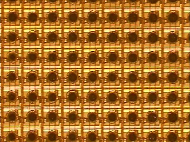
6 Flip chip bonding evolution 3 bonds/chip 1964 Cu ball transistor bonds/chip 1970 C4 SSIC 120 bonds/chip 1980 C4 LSI 354 bonds/chip 1985 C4 VLSI 2100 bonds/chip 2000 C4 SoC

 connections possible Improved high")


7 Flip chip bonding advantages Very high interconnection density Area array and peripheral bonds possible Fine pitch (50 m) connections possible Improved high frequency/speed performance Short/repeatable connection length Reduced electrical parasitics Minimal component footprint True chip scale package Pac Tech GmbH National Semiconductor Corp
8 Flip chip bonding technologies Solder flip chip Adhesive flip chip Solid phase flip chip
 Hybrid modules Typical flip chip in package Solder advantages Self aligning (<1")
9 Solder flip chip bonding Common uses Flip chip on board (FCOB) Flip chip in package (FCIP) System in package (SiP) Hybrid modules Typical flip chip in package Solder advantages Self aligning (<1 m)
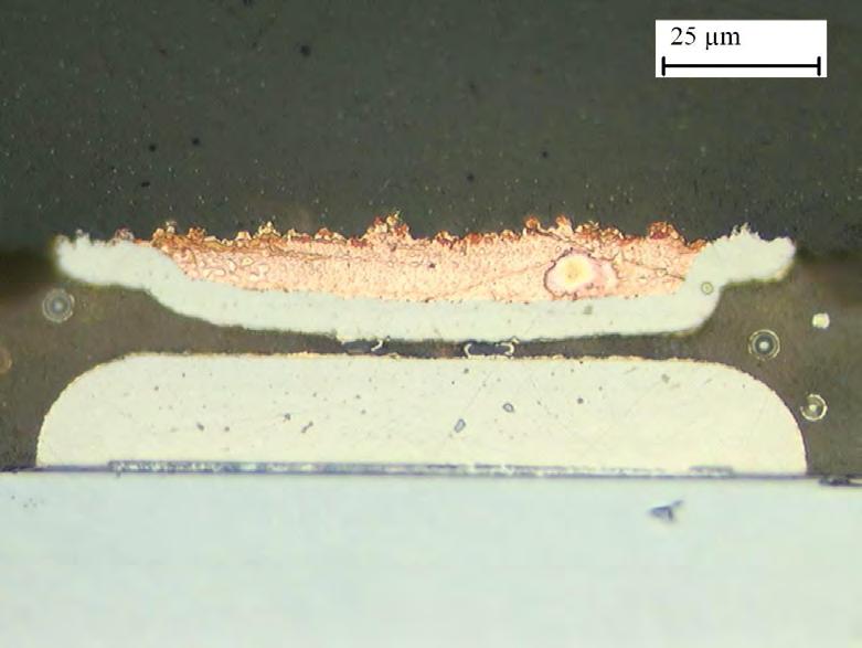
10 Solder flip chip bonding Bumping Bonding reflowed Device As deposited Pb CrCu/CuSn oxide AlSi passivation Device Substrate Controlled dewetting CrCuAu wettable metal 95Pb5Sn solder Limited wettable areas Surface tension controlled alignment stand-off
11 Solder flip chip bond design mg/n S p.a S Substrate Balance of surface tension & gravitational forces Conservation of volume allows joint design Surface tension dominates Double truncated sphere approximation Sets solder uniformity requirements, mixed bond design
12 Solder flip chip bond design = 0 o = 180 o Perimeter volume Solder volume uniformity requirements
13 Solder flip chip bond design As deposited reflowed bonded Matched 18 & 70 m bond design

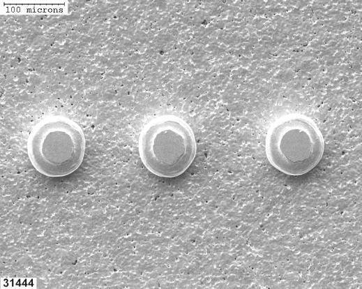
14 Solder flip chip bond alignment Solder vernier structure Alignment < 2 m vernier resolution

15 Solder bumping Wafer level processing Under bump metallisation (UBM) Ohmic contact Adhesion/barrier between the pad and the bump Wettable surface Common UBM deposition techniques Plating Evaporation Sputtering Typical UBMs Ni/Au Cr/CrCu/Cu/Au NiV/Cu TiW IC Interconnect
16 Solder bumping Typical solder alloys High melting point Lead/Tin (95/5) solder Eutectic Tin/Lead (63/37) solder Lead-free solder: Tin/Copper/Silver etc Eutectic Gold/Tin (80/20) solder Common solder deposition techniques Evaporation Plating Stencil printing Laser dispense Mould transfer IC Interconnect
17 Solder bumping underfill Required for flip chip on board (FCOB) reliability Underfill process underfill dispense underfill cure Dispense needle Underfill drawn under die by capillary action Flip Chip Integrated Circuit Laminate Printed Circuit Board


18 Solder bumping reliability Si substrate solder h d Low cycle thermal fatigue Factors Cycle amplitude Chip size CTE mismatch Solder alloy Bond geometry Use of underfill
 Low temperature process No separate underfill required (Anisotropic Conductive Adhesive)")
19 Adhesive flip chip bonding Common uses Chip on glass (COG) Chip on flex (COF) Adhesive advantages Fine pitch (50µm) Low temperature process No separate underfill required (Anisotropic Conductive Adhesive) Lead-free

 Hesse & Knipps Citizen Watch")
20 Adhesive flip chip wafer bumping Wafer level processing Common bump deposition techniques Gold stud bumps formed with a gold ball bonder Electroless plated nickel bumps/thin immersion gold Electrolytic plated gold bumps, typically on a TiW UBM Polymer bumps (selectively placed conducting adhesive) Hesse & Knipps Citizen Watch Co., Ltd.
21 Adhesive flip chip bonding Heated pick-up tool Anisotropic Conductive Film (conductive particles in a non-conductive adhesive) Integrated Circuit Die Substrate

22 Adhesive flip chip bonding
 Hybrid modules Die pads require bumping Gold stud bumps Electroplated gold bumps Hesse &")
23 Solid phase flip chip bonding Common uses Flip chip on board (FCOB) Flip chip in package (FCIP) System in package (SIP) Hybrid modules Die pads require bumping Gold stud bumps Electroplated gold bumps Hesse & Knipps

24 Solid phase bonding processes Heat, compression Heat, compression, ultrasonic vibration Hesse & Knipps Thermocompression Thermosonic Hesse & Knipps

25 Solid phase bump coining Individual/gang coining
26 Solder flip chip bond properties Bonding Parameter Wire Bond TAB Flip Chip Material(s) Al Au Cu Pb-Sn Melting temperature, o C or 183 Typical bond geometry 25 m diameter x 2.5mm length 25x100 m tape x 2.5mm length Typical pitch, m 100 m perimeter 200 m perimeter 200 m area Bond strength, grams Bond resistance, m.ohms Interbond capacitance, pf Bond inductance, nh <0.2 Thermal resistance o C/mW per bond No. of I/Os per chip 4mm chip size 8mm chip size m diameter 80 m height


27 Flip chip industry infrastructure Wafer bumping Over 20 companies established Flip chip substrates ~ 20 companies established Flip chip equipment Over 20 manufacturers established Flip chip assembly services Over 30 subcontractors Tyco Electronics
28 Flip chip applications Silicon devices Discretes RFICs - SiGe ASICs, Microprocessors & System-on-Chip GaAs devices Integrated Passive Devices (IPDs) System-in-Package (SiPs) 3D Integration Photonics Assemblies device and substrate alignment spatial light modulator Sensors Uncooled, cooled IR sensors HDD readers


29 Flip chip discretes Source: National Semiconductor.


30 Flip chip on lead SOT23 MLP Source: Carsem.

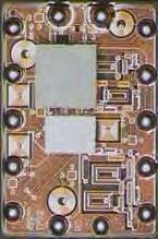
31 Flip chip RFIC Bluetooth Radio Module RF IC: 46 flip chip bonds at 200 m pitch Thin film integrated passives substrate 40 BGA balls at 0.80mm pitch Source: Intarsia.

32 Flip chip CPU IC Pentium II chip : 2100 flip chip bonds at 250 m pitch BGA substrate 570 BGA balls at 1.27mm pitch mini-cartridge substrate 240 way connector Source: Intel


33 Source:GMMT Flip chip GaAs


34 Flip chip IPDs Source:CMD Source: Telephus

35 Flip chip SiPs Source: Intarsia. Source: STMicroelectronics
36 Flip chip SiP utilisation SiP technologies - die level bare die CSP Other 2D 3D wire bond flip chip solder ball TSV die packaging die placement die interconnection Source: ektn

37 Flip chip 3D integration Source: inemi, IMEC

38 Flip chip 3D integration Source: inemi, Renesas
 560μm TSV")

39 Flip chip 3D integration 16Gb memory (8 x 2Gb) 560μm TSV Micro bump 50μm thick Chip Laser drilled via Source: inemi, Samsung

40 Source: GMMT Flip chip photonics devices


41 Flip chip IR sensor devices Source: Irisys

42 Flip chip hard disc sensor devices Source: Seagate


43 Flip Chip Trends Much wider uptake 2% to 10% all devices IPDs & high I/O devices Growth of infrastructure New technologies Cu pillar bumping Lower cost processes Finer pitch Chip-to-chip bonding Improved reliability Source: TechSearch International, Inc. Flip Chip Bonding Source: ChipWorks


44 Flip Chip Futures Flip chip usage will continue to grow Drivers High I/O applications Where size is critical High frequency/speed applications IPDs, SiPs, 3D integration Flip Chip Bonding

45 Thank you for your attention David Pedder David Pedder Associates 18, Ock Meadow, Stanford in the Vale Faringdon, Oxfordshire SN7 8LN +44 (0) (0)
B. Flip-Chip Technology
 B. Flip-Chip Technology B1. Level 1. Introduction to Flip-Chip techniques B1.1 Why flip-chip? In the development of packaging of electronics the aim is to lower cost, increase the packaging density, improve
Laser Solder Attach for Optoelectronics Packages
 1 Laser Solder Attach for Optoelectronics Packages Elke Zakel, Lars Titerle, Thomas Oppert, Ronald G. Blankenhorn* Pac Tech Packaging Technologies GmbH Am Schlangenhorst 15-17, Germany Phone:+ 49 (0) 33
!"#$"%&' ()#*+,-+.&/0(
#*+,-+.&/0(") !"#$"%&' ()#*+,-+.&/0( Multi Chip Modules (MCM) or Multi chip packaging Industry s first MCM from IBM. Generally MCMs are horizontal or two-dimensional modules. Defined as a single unit containing two
!"#$"%&' ()#*+,-+.&/0( Multi Chip Modules (MCM) or Multi chip packaging Industry s first MCM from IBM. Generally MCMs are horizontal or two-dimensional modules. Defined as a single unit containing two
Tape Automated Bonding
 Tape Automated Bonding Introduction TAB evolved from the minimod project begun at General Electric in 1965, and the term Tape Automated Bonding was coined by Gerard Dehaine of Honeywell Bull in 1971. The
"Low Cost Electroless Bumping for Ultra Fine Pitch Applications in 8" and 12" Wafers"
 1 "Low Cost Electroless Bumping for Ultra Fine Pitch Applications in 8" and 12" Wafers" Elke Zakel, Thomas Oppert, Ghassem Azdasht, Thorsten Teutsch * Pac Tech Packaging Technologies GmbH Am Schlangenhorst
POSSUM TM Die Design as a Low Cost 3D Packaging Alternative
 POSSUM TM Die Design as a Low Cost 3D Packaging Alternative The trend toward 3D system integration in a small form factor has accelerated even more with the introduction of smartphones and tablets. Integration
23. Packaging of Electronic Equipments (2)
") 23. Packaging of Electronic Equipments (2) 23.1 Packaging and Interconnection Techniques Introduction Electronic packaging, which for many years was only an afterthought in the design and manufacture of
23. Packaging of Electronic Equipments (2) 23.1 Packaging and Interconnection Techniques Introduction Electronic packaging, which for many years was only an afterthought in the design and manufacture of
Benzocyclobutene Polymer dielectric from Dow Chemical used for wafer-level redistribution.
 Glossary of Advanced Packaging: ACA Bare Die BCB BGA BLT BT C4 CBGA CCC CCGA CDIP or CerDIP CLCC COB COF CPGA Anisotropic Conductive Adhesive Adhesive with conducting filler particles where the electrical
Application Note AN-1011
 AN-1011 Board Mounting Application Note for 0.800mm Pitch Devices For part numbers IRF6100, IRF6100PBF, IR130CSP, IR130CSPPBF, IR140CSP, IR140CSPPBF, IR1H40CSP, IR1H40CSPPBF By Hazel Schofield and Philip
Chapter 2. Literature Review
 Chapter 2 Literature Review 2.1 Development of Electronic Packaging Electronic Packaging is to assemble an integrated circuit device with specific function and to connect with other electronic devices.
Electroless Bumping for 300mm Wafers
 Electroless Bumping for 300mm Wafers T. Oppert Internepcon 2006 Tokyo Big Sight, Japan Outline Short Company Profile Electroless Ni/Au Under Bump Metallization UBM for Copper Devices Solder Bumping: Stencil
9 CHIP BONDING AT THE FIRST LEVEL
 9 CHIP BONDING AT THE FIRST LEVEL The I/O interface to the die primarily interconnects electrical power, ground and signals. It must provide for low impedance for the power distribution system, so as to
EMERGING SUBSTRATE TECHNOLOGIES FOR PACKAGING
 EMERGING SUBSTRATE TECHNOLOGIES FOR PACKAGING Henry H. Utsunomiya Interconnection Technologies, Inc. Suwa City, Nagano Prefecture, Japan henryutsunomiya@mac.com ABSTRACT This presentation will outline
Advanced Packaging - Pulsed-laser Heating for Flip Chip Assembly
 Page 1 of 5 Pulsed-laser Heating for Flip Chip Assembly A stress-free alternative By Thorsten Teutsch, Ph.D., Pac Tech USA, Elke Zakel, Ph.D., and Ghassem Azdasht, Pac Tech GmbH As flip chip applications
Flip-Chip for MM-Wave and Broadband Packaging
 1 Flip-Chip for MM-Wave and Broadband Packaging Wolfgang Heinrich Ferdinand-Braun-Institut für Höchstfrequenztechnik (FBH) Berlin / Germany with contributions by F. J. Schmückle Motivation Growing markets
50 Micron Pitch Flip Chip Bumping Technology: Processes and Applications
 50 Micron Pitch Flip Chip Bumping Technology: Processes and Applications Alan Huffman Center for Materials and Electronic Technologies huffman@rti.org Outline RTI Identity/History Historical development
سمینار درس تئوری و تکنولوژی ساخت
 نام خدا به 1 سمینار درس تئوری و تکنولوژی ساخت Wire Bonding استاد : جناب آقای محمدنژاد دکتر اردیبهشت 93 2 3 Content IC interconnection technologies Whats wirebonding Wire Bonding Processes Thermosonic Wirebond
Laser Assisted Flip Chip Assembly for LCD Applications using ACP and NCP Adhesive Joining
 1 Laser Assisted Flip Chip Assembly for LCD Applications using ACP and NCP Adhesive Joining Elke Zakel, Ghassem Azdasht, Thorsten Teutsch *, Ronald G. Blankenhorn* Pac Tech Packaging Technologies GmbH
The Future of Packaging ~ Advanced System Integration
 The Future of Packaging ~ Advanced System Integration Enabling a Microelectronic World R. Huemoeller SVP, Adv. Product / Platform Develop June 2013 Product Segments End Market % Share Summary 2 New Product
SOLDER BUMP FLIP CHIP BONDING FOR PIXEL DETECTOR HYBRIDIZATION
 SOLDER BUMP FLIP CHIP BONDING FOR PIXEL DETECTOR HYBRIDIZATION Jorma Salmi and Jaakko Salonen VTT Information Technology Microelectronics P.O. Box 1208 FIN-02044 VTT, Finland (visiting: Micronova, Tietotie
Flip Chip Bonding Using Sony Anisotropic Conductive Film (ACF) FP1526Y
 FP1526Y") Flip Chip Bonding Using Sony Anisotropic Conductive Film (ACF) FP1526Y Purpose: Author: Rekha S. Pai (07/29/03) To use ACF as an interconnection method for attaching dice to substrates. Direct electrical
Flip Chip Bonding Using Sony Anisotropic Conductive Film (ACF) FP1526Y Purpose: Author: Rekha S. Pai (07/29/03) To use ACF as an interconnection method for attaching dice to substrates. Direct electrical
Introduction of IMS Technology for Advanced Solder Bumping on Wafers / Laminates
 Introduction of IMS Technology for Advanced Solder Bumping on Wafers / Laminates Science & Technology IBM Research Tokyo Yasumitsu Orii, PhD Senju Metal Industry Co.,TW Deputy General Manager Lewis Huang
Two major features of this text
 Two major features of this text Since explanatory materials are systematically made based on subject examination questions, preparation
Flip Chip Bumping & Assembly
 6. Europäisches Elektroniktechnologie-Kolleg 19.-23. März 2003 Colonia de Sant Jordi, Mallorca - Club Colonia Sant Jordi Flip Chip Bumping & Assembly Hermann Oppermann Fraunhofer IZM, Berlin Gustav-Meyer-Allee
NEW PACKAGING AND INTERCONNECT TECHNOLOGIES FOR ULTRA THIN CHIPS
 NEW PACKAGING AND INTERCONNECT TECHNOLOGIES FOR ULTRA THIN CHIPS Christine Kallmayer and Rolf Aschenbrenner Fraunhofer IZM Berlin, Germany kallmayer@izm.fhg.de Julian Haberland and Herbert Reichl Technical
64 Channel Flip-Chip Mounted Selectively Oxidized GaAs VCSEL Array
 64 Channel Flip-Chip Mounted Selectively Oxidized GaAs VCSEL Array 69 64 Channel Flip-Chip Mounted Selectively Oxidized GaAs VCSEL Array Roland Jäger and Christian Jung We have designed and fabricated
New Wave SiP solution for Power
 New Wave SiP solution for Power Vincent Lin Corporate R&D ASE Group APEC March 7 th, 2018 in San Antonio, Texas. 0 Outline Challenges Facing Human Society Energy, Environment and Traffic Autonomous Driving
UMS User guide for bare dies GaAs MMIC. storage, pick & place, die attach and wire bonding
 UMS User guide for bare dies GaAs MMIC storage, pick & place, die attach and wire bonding Ref. : AN00014097-07 Apr 14 1/10 Specifications subject to change without notice United Monolithic Semiconductors
Application Note 5026
 Surface Laminar Circuit (SLC) Ball Grid Array (BGA) Eutectic Surface Mount Assembly Application Note 5026 Introduction This document outlines the design and assembly guidelines for surface laminar circuitry
Processes for Flexible Electronic Systems
 Processes for Flexible Electronic Systems Michael Feil Fraunhofer Institut feil@izm-m.fraunhofer.de Outline Introduction Single sheet versus reel-to-reel (R2R) Substrate materials R2R printing processes
Assembly/Packagng RF-PCB. Thick Film. Thin Film. Screening/Test. Design Manual
 Thick Film Thin Film RF-PCB Assembly/Packagng Screening/Test Design Manual RHe Design Manual The following rules are effective for the draft of circuit boards and hybrid assemblies. The instructions are
SOLDERABLE ANISOTROPIC CONDUCTIVE ADHESIVES FOR 3D PACKAGE APPLICATIONS
 SOLDERABLE ANISOTROPIC CONDUCTIVE ADHESIVES FOR 3D PACKAGE APPLICATIONS ABSTRACT: Dr. Mary Liu and Dr. Wusheng Yin YINCAE Advanced Materials, LLC Albany, NY 3D packaging has recently become very attractive
Electronic materials and components-semiconductor packages
 Electronic materials and components-semiconductor packages Semiconductor back-end processes We will learn much more about semiconductor back end processes in subsequent modules, but you need to understand
AND8081/D. Flip Chip CSP Packages APPLICATION NOTE
 Flip Chip CSP Packages Prepared by: Denise Thienpont ON Semiconductor Staff Engineer APPLICATION NOTE Introduction to Chip Scale Packaging This application note provides guidelines for the use of Chip
Chapter 11 Testing, Assembly, and Packaging
 Chapter 11 Testing, Assembly, and Packaging Professor Paul K. Chu Testing The finished wafer is put on a holder and aligned for testing under a microscope Each chip on the wafer is inspected by a multiple-point
EUFANET Toulouse conferences, November 28th-29th, 2011 Stéphane Bellenger, IPDiA
 3D low-profile Silicon interposer using Passive Integration (PICS) and Advanced Packaging Solutions EUFANET Toulouse conferences, November 28th-29th, 2011 Stéphane Bellenger, IPDiA 3D Advanced Integration
Flip Chips. FA10-200x200 FA10-400x400 FA10-600x x 200 mils 400 x 400 mils
 Flip Chip FlipChip International Flip Chip describes the method of electrically connecting the die to the package carrier. The package carrier, either substrate or leadframe, then provides the connection
1. Exceeding these limits may cause permanent damage.
 Silicon PIN Diode s Features Switch & Attenuator Die Extensive Selection of I-Region Lengths Hermetic Glass Passivated CERMACHIP Oxide Passivated Planar s Voltage Ratings to 3000V Faster Switching Speed
IMAGE SENSOR EVOLUTION AND ENABLING 3D TECHNOLOGIES
 Fig. 5: Scanning Electron Microscopy images (TOP view, 3D view, Zoome including all metal levels of the BSI imager structure. (dashed line shows bonding IMAGE SENSOR EVOLUTION AND ENABLING 3D TECHNOLOGIES
Fraunhofer IZM - ASSID
 FRAUNHOFER-INSTITUT FÜR Zuverlässigkeit und Mikrointegration IZM Fraunhofer IZM - ASSID All Silicon System Integration Dresden Heterogeneous 3D Wafer Level System Integration 3D system integration is one
SiP packaging technology of intelligent sensor module. Tony li
 SiP packaging technology of intelligent sensor module Tony li 2016.9 Contents What we can do with sensors Sensor market trend Challenges of sensor packaging SiP technology to overcome challenges Overview
Innovations Push Package-on-Package Into New Markets. Flynn Carson. STATS ChipPAC Inc Kato Rd Fremont, CA 94538
 Innovations Push Package-on-Package Into New Markets by Flynn Carson STATS ChipPAC Inc. 47400 Kato Rd Fremont, CA 94538 Copyright 2010. Reprinted from Semiconductor International, April 2010. By choosing
Silicon Interposers enable high performance capacitors
 Interposers between ICs and package substrates that contain thin film capacitors have been used previously in order to improve circuit performance. However, with the interconnect inductance due to wire
MA4L Series. Silicon PIN Limiters RoHS Compliant. M/A-COM Products Rev. V12. Features. Chip Outline. Description. Applications
 Features Low Insertion Loss and Noise Figure High Peak and Average Operating Power Various P1dB Compression Powers Low Flat Leakage Power Proven Reliable, Silicon Nitride Passivation Chip Outline A Square
Getting the FLI Lead Out. Thomas J. De Bonis Assembly & Test Technology Development Technology and Manufacturing Group
 Getting the FLI Lead Out Thomas J. De Bonis Assembly & Test Technology Development Technology and Manufacturing Group Lead has been used in flip chip FLI for decades. RoHS Exemption 15 was enacted in recognition
Flip Chip Installation using AT-GDP Rework Station
 Flip Chip Installation using AT-GDP Rework Station Introduction An increase in implementation of Flip Chips, Dies, and other micro SMD devices with hidden joints within PCB and IC assembly sectors requires
Chemnitzer Seminar System Integration Technologies. Solder Jetting, Rework & electroless UBM Deposition
 Chemnitzer Seminar System Integration Technologies June 14 15, 2016 Solder Jetting, Rework & electroless UBM Deposition Made in Germany PacTech Group - Milestones 1995 PacTech founded in Berlin, Germany
WLCSP and FlipChip Production Bumping Using Electroless Ni/Au Plating And Wafer Level Solder Sphere Transfer Technologies
 WLCSP and FlipChip Production Bumping Using Electroless Ni/Au Plating And Wafer Level Solder Sphere Transfer Technologies Andrew Strandjord, Jing Li, Axel Scheffler, and Thorsten Teutsch PacTech - Packaging
Packaging Roadmap: The impact of miniaturization. Bob Pfahl, inemi Celestica-iNEMI Technology Forum May 15, 2007
 Packaging Roadmap: The impact of miniaturization Bob Pfahl, inemi Celestica-iNEMI Technology Forum May 15, 2007 The Challenges for the Next Decade Addressing the consumer experience using the converged
TSV MEOL (Mid-End-Of-Line) and its Assembly/Packaging Technology for 3D/2.5D Solutions
 and its Assembly/Packaging Technology for 3D/2.5D Solutions") TSV MEOL (Mid-End-Of-Line) and its Assembly/Packaging Technology for 3D/2.5D Solutions Seung Wook YOON, D.J. Na, *K. T. Kang, W. K. Choi, C.B. Yong, *Y.C. Kim and Pandi C. Marimuthu STATS ChipPAC Ltd.
TSV MEOL (Mid-End-Of-Line) and its Assembly/Packaging Technology for 3D/2.5D Solutions Seung Wook YOON, D.J. Na, *K. T. Kang, W. K. Choi, C.B. Yong, *Y.C. Kim and Pandi C. Marimuthu STATS ChipPAC Ltd.
Silicon PIN Limiter Diodes V 5.0
 5 Features Lower Insertion Loss and Noise Figure Higher Peak and Average Operating Power Various P1dB Compression Powers Lower Flat Leakage Power Reliable Silicon Nitride Passivation Description M/A-COM
Application Bulletin 240
 Application Bulletin 240 Design Consideration CUSTOM CAPABILITIES Standard PC board fabrication flexibility allows for various component orientations, mounting features, and interconnect schemes. The starting
TAIPRO Engineering. Speaker: M. Saint-Mard Managing director. TAIlored microsystem improving your PROduct
 TAIPRO Engineering MEMS packaging is crucial for system performance and reliability Speaker: M. Saint-Mard Managing director TAIPRO ENGINEERING SA Michel Saint-Mard Administrateur délégué m.saintmard@taipro.be
Flexline - A Flexible Manufacturing Method for Wafer Level Packages (Extended Abstract)
") Flexline - A Flexible Manufacturing Method for Wafer Level Packages (Extended Abstract) by Tom Strothmann, *Damien Pricolo, **Seung Wook Yoon, **Yaojian Lin STATS ChipPAC Inc.1711 W Greentree Drive Tempe,
Flexline - A Flexible Manufacturing Method for Wafer Level Packages (Extended Abstract) by Tom Strothmann, *Damien Pricolo, **Seung Wook Yoon, **Yaojian Lin STATS ChipPAC Inc.1711 W Greentree Drive Tempe,
The Future of Packaging and Cu Wire Bonding Advances. Ivy Qin
 The Future of Packaging and Cu Wire Bonding Advances Ivy Qin Introduction Semiconductors have been around for over 70 years Packaging is playing a more and more important role, providing low cost high
An Introduction to Electronics Systems Packaging. Prof. G. V. Mahesh. Department of Electronic Systems Engineering
 An Introduction to Electronics Systems Packaging Prof. G. V. Mahesh Department of Electronic Systems Engineering India Institute of Science, Bangalore Module No. # 02 Lecture No. # 08 Wafer Packaging Packaging
Winter College on Optics: Fundamentals of Photonics - Theory, Devices and Applications February 2014
 2572-10 Winter College on Optics: Fundamentals of Photonics - Theory, Devices and Applications 10-21 February 2014 Photonic packaging and integration technologies II Sonia M. García Blanco University of
Low Thermal Resistance Flip-Chip Bonding of 850nm 2-D VCSEL Arrays Capable of 10 Gbit/s/ch Operation
 Low Thermal Resistance Flip-Chip Bonding of 85nm -D VCSEL Arrays Capable of 1 Gbit/s/ch Operation Hendrik Roscher In 3, our well established technology of flip-chip mounted -D 85 nm backside-emitting VCSEL
High Efficient Heat Dissipation on Printed Circuit Boards. Markus Wille, R&D Manager, Schoeller Electronics Systems GmbH
 High Efficient Heat Dissipation on Printed Circuit Boards Markus Wille, R&D Manager, Schoeller Electronics Systems GmbH m.wille@se-pcb.de Introduction 2 Heat Flux: Q x y Q z The substrate (insulation)
Study on Solder Joint Reliability of Fine Pitch CSP
 As originally published in the IPC APEX EXPO Conference Proceedings. Study on Solder Joint Reliability of Fine Pitch CSP Yong (Hill) Liang, Hank Mao, YongGang Yan, Jindong (King) Lee. AEG, Flextronics
Figure 1. FCBGA and fccsp Packages
 Packaging Technology and Design Challenge for Fine Pitch Micro-Bump Cu-Pillar and BOT (Direct Bond on Substrate-Trace) Using TCNCP (Thermal Compression with Non-Conductive Paste Underfill) Method *MJ (Myung-June)
CHAPTER 11: Testing, Assembly, and Packaging
 Chapter 11 1 CHAPTER 11: Testing, Assembly, and Packaging The previous chapters focus on the fabrication of devices in silicon or the frontend technology. Hundreds of chips can be built on a single wafer,
MICROELECTRONICS ASSSEMBLY TECHNOLOGIES. The QFN Platform as a Chip Packaging Foundation
 West Coast Luncheon January 15, 2014. PROMEX PROMEX INDUSTRIES INC. MICROELECTRONICS ASSSEMBLY TECHNOLOGIES The QFN Platform as a Chip Packaging Foundation 3075 Oakmead Village Drive Santa Clara CA Ɩ 95051
Image Sensor Advanced Package Solution. Prepared by : JL Huang & KingPak RD division
 Image Sensor Advanced Package Solution Prepared by : JL Huang & KingPak RD division Contents CMOS image sensor marketing overview Comparison between different type of CMOS image sensor package Overview
Advanced Packaging Equipment Solder Jetting & Laser Bonding
 Advanced Packaging Equipment Solder Jetting & Laser Bonding www.pactech.comw.pactech.com PacTech Packaging Technologies Pioneering in laser solder jetting technologies since 1995 Our mission is to reshape
Product Catalog. Semiconductor Intellectual Property & Technology Licensing Program
 Product Catalog Semiconductor Intellectual Property & Technology Licensing Program MANUFACTURING PROCESS TECHNOLOGY OVERVIEW 90 nm 130 nm 0.18 µm 0.25 µm 0.35 µm >0.40 µm Logic CMOS SOI CMOS SOI CMOS SOI
BGA (Ball Grid Array)
") BGA (Ball Grid Array) National Semiconductor Application Note 1126 November 2002 Table of Contents Introduction... 2 Package Overview... 3 PBGA (PLASTIC BGA) CONSTRUCTION... 3 TE-PBGA (THERMALLY ENHANCED
BGA (Ball Grid Array) National Semiconductor Application Note 1126 November 2002 Table of Contents Introduction... 2 Package Overview... 3 PBGA (PLASTIC BGA) CONSTRUCTION... 3 TE-PBGA (THERMALLY ENHANCED
CHAPTER I. Introduction. 1.1 Overview of Power Electronics Packaging
 CHAPTER I Introduction 1.1 Overview of Power Electronics Packaging Basically, power electronics packages provide mechanical support, device protection, cooling and electrical connection and isolation for
Smart Devices of 2025
 Smart Devices of 2025 Challenges for Packaging of Future Device Technologies Steve Riches/Kevin Cannon Tribus-D Ltd CW Workshop 27 March 2018 E:mail: info@tribus-d.uk M: 07804 980 954 Assembly Technology
BGA/CSP Re-balling Bob Doetzer Circuit Technology Inc.
 BGA/CSP Re-balling Bob Doetzer Circuit Technology Inc. www.circuittechnology.com The trend in the electronics interconnect industry towards Area Array Packages type packages (BGA s, CSP s, CGA s etc.)
Through Glass Via (TGV) Technology for RF Applications
 Technology for RF Applications") Through Glass Via (TGV) Technology for RF Applications C. H. Yun 1, S. Kuramochi 2, and A. B. Shorey 3 1 Qualcomm Technologies, Inc. 5775 Morehouse Dr., San Diego, California 92121, USA Ph: +1-858-651-5449,
Through Glass Via (TGV) Technology for RF Applications C. H. Yun 1, S. Kuramochi 2, and A. B. Shorey 3 1 Qualcomm Technologies, Inc. 5775 Morehouse Dr., San Diego, California 92121, USA Ph: +1-858-651-5449,
APPLICATION NOTE 6381 ORGANIC LAND GRID ARRAY (OLGA) AND ITS APPLICATIONS
 AND ITS APPLICATIONS") Keywords: OLGA, SMT, PCB design APPLICATION NOTE 6381 ORGANIC LAND GRID ARRAY (OLGA) AND ITS APPLICATIONS Abstract: This application note discusses Maxim Integrated s OLGA and provides the PCB design and
Keywords: OLGA, SMT, PCB design APPLICATION NOTE 6381 ORGANIC LAND GRID ARRAY (OLGA) AND ITS APPLICATIONS Abstract: This application note discusses Maxim Integrated s OLGA and provides the PCB design and
MASW P. SURMOUNT PIN Diode Switch Element with Thermal Terminal. Features. Description. Ordering Information 2.
 Features Specified Bandwidth: 45MHz 2.5GHz Useable 30MHz to 3.0GHz Low Loss 40dB High C.W. Incident Power, 50W at 500MHz High Input IP3, +66dBm @ 500MHz Unique Thermal Terminal for
Flip chip Assembly with Sub-micron 3D Re-alignment via Solder Surface Tension
 Flip chip Assembly with Sub-micron 3D Re-alignment via Solder Surface Tension Jae-Woong Nah*, Yves Martin, Swetha Kamlapurkar, Sebastian Engelmann, Robert L. Bruce, and Tymon Barwicz IBM T. J. Watson Research
Market and technology trends in advanced packaging
 Close Market and technology trends in advanced packaging Executive OVERVIEW Recent advances in device miniaturization trends have placed stringent requirements for all aspects of product manufacturing.
mcube WLCSP Application Note
 AN-002 Rev.02 mcube WLCSP Application Note AN-002 Rev.02 mcube, Inc. 1 / 20 AN-002 Rev.02 Guidelines for Printed Circuit Board (PCB) Design and Assembly with mcube Wafer Level Chip Scale Package (WLCSP)
Chip Assembly on MID (Molded Interconnect Device) A Path to Chip Modules with increased Functionality
 A Path to Chip Modules with increased Functionality") T e c h n o l o g y Dr. Werner Hunziker Chip Assembly on MID (Molded Interconnect Device) A Path to Chip Modules with increased Functionality The MID (Molded Interconnect Device) technology enables the
T e c h n o l o g y Dr. Werner Hunziker Chip Assembly on MID (Molded Interconnect Device) A Path to Chip Modules with increased Functionality The MID (Molded Interconnect Device) technology enables the
SFC3.3-4 Low Voltage ChipClamp ΤΜ Flip Chip TVS Diode Array
 Description The SFC3.3-4 is a quad flip chip TS diode array. They are state-of-the-art devices that utilize solid-state EPD TS technology for superior clamping performance and DC electrical characteristics.
Challenges of Evolving Technology in the Workplace. Tips. Bubba Powers. Board Density. Best Rework Soldering Practices. Power. Substrates.
 Real Estate Finishes Power Component Technology Board Density Tips Challenges of Evolving Technology in the Workplace Substrates Component Size Bubba Powers Manager of Technical Services Weller North America
PAGE 1/6 ISSUE SERIES Micro-SPDT PART NUMBER R516 XXX 10X. (All dimensions are in mm [inches]) R 516 _ 1 0 _
![PAGE 1/6 ISSUE SERIES Micro-SPDT PART NUMBER R516 XXX 10X. (All dimensions are in mm [inches]) R 516 _ 1 0 _](/thumbs/96/127769340.jpg "PAGE 1/6 ISSUE SERIES Micro-SPDT PART NUMBER R516 XXX 10X. (All dimensions are in mm [inches]) R 516 _ 1 0 _") PAGE 1/6 ISSUE 15-10-18 SERIES Micro-SPDT PART NUMBER R516 XXX 10X R516 series: the RAMSES concept merges with the SLIM LINE technology, breaking up the frequency limits of SMT switches : - FULL SMT TECHNOLOGY
PAGE 1/6 ISSUE 15-10-18 SERIES Micro-SPDT PART NUMBER R516 XXX 10X R516 series: the RAMSES concept merges with the SLIM LINE technology, breaking up the frequency limits of SMT switches : - FULL SMT TECHNOLOGY
Laminate Based Fan-Out Embedded Die Technologies: The Other Option
 Laminate Based Fan-Out Embedded Die Technologies: The Other Option Theodore (Ted) G. Tessier, Tanja Karila*, Tuomas Waris*, Mark Dhaenens and David Clark FlipChip International, LLC 3701 E University Drive
Integration of 3D detector systems
 Integration of 3D detector systems Piet De Moor Introduction Evolution in radiation detection/imaging: single pixel linear array 2D array increase in resolution = decrease in pitch (down to few um) = thanks
PAGE 1/6 ISSUE Jul SERIES Micro-SPDT PART NUMBER R516 XXX 10X R 516 _ 1 0 _
 PAGE 1/6 ISSUE Jul-24-2017 SERIES Micro-SPDT PART NUMBER R516 XXX 10X R516 series: the RAMSES concept merges with the SLIM LINE technology, breaking up the frequency limits of SMT switches : - FULL SMT
New Approaches to Develop a Scalable 3D IC Assembly Method
 New Approaches to Develop a Scalable 3D IC Assembly Method Charles G. Woychik Ph.D. Sangil Lee, Ph.D., Scott McGrath, Eric Tosaya and Sitaram Arkalgud Ph.D. Invensas Corporation 3025 Orchard Parkway San
Carbon Nanotube Bumps for Thermal and Electric Conduction in Transistor
 Carbon Nanotube Bumps for Thermal and Electric Conduction in Transistor V Taisuke Iwai V Yuji Awano (Manuscript received April 9, 07) The continuous miniaturization of semiconductor chips has rapidly improved
Assembly Instructions for SCC1XX0 series
 Technical Note 82 Assembly Instructions for SCC1XX0 series TABLE OF CONTENTS Table of Contents...1 1 Objective...2 2 VTI's 32-lead Dual In-line Package (DIL-32)...2 3 DIL-32 Package Outline and Dimensions...2
Min Tao, Ph. D, Ashok Prabhu, Akash Agrawal, Ilyas Mohammed, Ph. D, Bel Haba, Ph. D Oct , IWLPC
 PACKAGE-ON-PACKAGE INTERCONNECT FOR FAN-OUT WAFER LEVEL PACKAGES Min Tao, Ph. D, Ashok Prabhu, Akash Agrawal, Ilyas Mohammed, Ph. D, Bel Haba, Ph. D Oct 18-20 2016, IWLPC 1 Outline Laminate to Fan-Out
WAFER-LEVEL SOLDER SPHERE PLACEMENT AND ITS IMPLICATIONS
 WAFER-LEVEL SOLDER SPHERE PLACEMENT AND ITS IMPLICATIONS Andrew Strandjord, Thomas Oppert, Thorsten Teutsch, and Ghassem Azdasht PacTech - Packaging Technologies, Inc. Am Schlangenhorst 15-17 14641 Nauen,
EMBEDDED ACTIVE DEVICE PACKAGING TECHNOLOGY FOR REAL DDR2 MEMORY CHIPS
 EMBEDDED ACTIVE DEVICE PACKAGING TECHNOLOGY FOR REAL DDR2 MEMORY CHIPS Yin-Po Hung, Tao-Chih Chang, Ching-Kuan Lee, Yuan-Chang Lee, Jing-Yao Chang, Chao-Kai Hsu, Shu-Man Li, Jui-Hsiung Huang, Fang-Jun
Power Integration in Circuit Board
 Power Integration in Circuit Board APEC 2015 AT & S Austria Technologie & Systemtechnik Aktiengesellschaft Fabriksgasse13 A-8700 Leoben Tel +43 (0) 3842 200-0 E-Mail info@ats.net www.ats.net PICB APEC
Wafer Level System Integration. Oswin Ehrmann
 Wafer Level System Integration Oswin Ehrmann Fraunhofer Institut for Reliability and Microintegration IZM D-13355 Berlin Germany Gustav-Meyer-Allee 25 Outline Introduction Wafer Bumping and Flip Chip Bonding
Assembly Instructions for SCA6x0 and SCA10x0 series
 Technical Note 71 Assembly Instructions for SCA6x0 and SCA10x0 series TABLE OF CONTENTS Table of Contents...1 1 Objective...2 2 VTI'S DIL-8 and DIL-12 packages...2 3 Package Outline and Dimensions...2
Off-Chip Interconnects in Wireless Hardware a tutorial : technologies and trends
 Off-Chip Interconnects in Wireless Hardware a tutorial : technologies and trends by Jan Hesselbarth, University of Stuttgart FP7 ARTISAN training, Belfast, October 27, 2014 Outline: Introduction Solder
Lecture: Integration of silicon photonics with electronics. Prepared by Jean-Marc FEDELI CEA-LETI
 Lecture: Integration of silicon photonics with electronics Prepared by Jean-Marc FEDELI CEA-LETI Context The goal is to give optical functionalities to electronics integrated circuit (EIC) The objectives
Brief Introduction of Sigurd IC package Assembly
 Brief Introduction of Sigurd IC package Assembly Content Package Development Trend Product Brief Sawing type QFN Representative MEMS Product LGA Light Sensor Proximity Sensor High Yield Capability Low
Compression Molding. Solutions for 3D TSV and other advanced packages as well as cost savings for standard package applications
 Compression Molding Solutions for 3D TSV and other advanced packages as well as cost savings for standard package applications 1. Company Introduction 2. Package Development Trend 3. Compression FFT Molding
The 3D Silicon Leader
 The 3D Silicon Leader 3D Silicon IPD for smaller and more reliable Implantable Medical Devices ATW on Advanced Packaging for Wireless Medical Devices Mohamed Mehdi Jatlaoui, Sébastien Leruez, Olivier Gaborieau,
Opportunities and challenges of silicon photonics based System-In-Package
 Opportunities and challenges of silicon photonics based System-In-Package ECTC 2014 Panel session : Emerging Technologies and Market Trends of Silicon Photonics Speaker : Stéphane Bernabé (Leti Photonics
Enabling concepts: Packaging Technologies
 Enabling concepts: Packaging Technologies Ana Collado / Liam Murphy ESA / TEC-EDC 01/10/2018 ESA UNCLASSIFIED - For Official Use Enabling concepts: Packaging Technologies Drivers for the future: Higher
Packaging Technology and Design Challenges for Fine Pitch Cu Pillar and BOT (Bond on Trace) using Thermal Compression Bonding
 using Thermal Compression Bonding") Packaging Technology and Design Challenges for Fine Pitch Cu Pillar and BOT (Bond on Trace) using Thermal Compression Bonding MJ (Myung-June) Lee 1, Chew Ching Lim 2, Pheak Ti Teh 2 1: Altera Corporation,
Packaging Technology and Design Challenges for Fine Pitch Cu Pillar and BOT (Bond on Trace) using Thermal Compression Bonding MJ (Myung-June) Lee 1, Chew Ching Lim 2, Pheak Ti Teh 2 1: Altera Corporation,