Figure 1. FCBGA and fccsp Packages
|
|
|
- Rosalind Stanley
- 6 years ago
- Views:
Transcription
1 Packaging Technology and Design Challenge for Fine Pitch Micro-Bump Cu-Pillar and BOT (Direct Bond on Substrate-Trace) Using TCNCP (Thermal Compression with Non-Conductive Paste Underfill) Method *MJ (Myung-June) Lee Altera Corporation **SungSoon Park, DongSu Ryu, MinJae Lee Amkor Technology Inc. ***Hank (Hajime) Saiki, Seiji Mori, Makoto Nagai NTK Technologies, Inc *Altera Corporation, 101 Innovation Drive, San Jose, CA U.S.A. **Amkor Technology Korea Inc , 2-ga, Seongsu-dong, Seongdong-gu, Seoul, Korea ***NTK Technology, 3979 Freedom Circle, Suite 320, Santa Clara, CA U.S.A. ABSTRACT The companies writing this paper have jointly developed Copper (Cu) Pillar micro-bump and TCNCP(Thermal Compression with Non-Conductive Paste) technology over the last two+ years. The Cu Pillar micro-bump and TCNCP is one of the platform technologies, which is essentially required for 2.5D/3D chip stacking as well as cost effective SFF (small form factor) package enablement. Although the baseline packaging process methodology for a normal pad pitch (i.e. inline 50µm) within smaller chip size (i.e. 100 mm 2 ) has been established and are in use for HVM production, there are several challenges to be addressed for further development for commercialization of finer bump pitch with larger die (i.e. 50µm tri-tier bond pad with the die larger than 400mm 2 ). This paper will address the key challenges of each field, such as the Cu trace design on a substrate for robust microjoint reliability, TCNCP technology, and substrate technology (i.e. structure, surface finish). Technical recommendations based on the lessons learned from a series of process experimentation will be provided, as well. Finally, this technology has been used for the successful launching of the company FPGA products with SFF packaging technology. Keywords Copper pillar, Micro-bump, TCNCP (Thermal Compression and Non-Conductive Paste), SFF (Small Form Factor), RDL (Re- Distribution Layers), UBM (Under Bump Metallization), SAM (Scanning Acoustic Microscopy), DFM (Design for Manufacturing), DR (Design Rule), POR (Plan of Record), BOM (Bill of Material), isro (Isolate Solder Resist Opening) 1. Introduction As Copper (Cu) pillar bump technology becomes more mature, it is gradually taking the place of the conventional solder base bump in flip chip interconnections, especially in devices requiring a finer bump pitch less than 150~130µm down to 40µm. A typical Cu bump is composed of Cu column (pillar) base and solder cap. A columnar Cu base can be a circular or ovular shape, and the solder cap, typically composed of a Tin/Silver (SnAg) solder alloy, which is plated on top of the Cu column. Several motivating facts that drives Cu bump over solder bump are the superiority of mechanical endurance, electrical performance, and the packaging assembly manufacturability for finer pitch devices. The mechanical durability of Cu helps to improve the bump reliability from joint fatigue failure. Decreasing the bump pitch triggers a higher risk of electro-migration by increasing the density of the electrical current and thermal energy in the flip chip interconnection, but the Cu bump is enough to compensate for the weakness of the solder bump. The finer pitch scaling capability of the Cu bump can also help to reduce the bump bridge issue at the flip chip attach manufacturing process compared with the solder bump. Another favorable output from the implementation of the Cu bump is satisfying EU and Industry ROHS-6 requirements by achieving Pb-free bump compliance with minimal effort. Another field in which the fine pitch Cu-pillar technology is gradually replacing is the chip-to-package interconnection using wire bonding technology. Dominant among several challenges on wire bonding interconnection are the limitation of physicalmechanical coverage and electrical performance. The physical-mechanical limitation comes from the complicated wire bond

2 design rule (i.e. wire angle, length, loop control, bond pad, and finger dimension per wire size) which results in a limited IO density of wire bond devices and gates to achieve package miniaturization. It is a well known fact that enabling the Fine Pitch Cu Pillar Technology is the most effective way of solving these issues and challenges while achieving a higher IO density within the smallest form factor package possible and improving electrical performance. This paper will mainly discuss the challenges on packaging process technology: how to engineer a Cu pillar structure, how to decide substrate structure (i.e. bond on trace) and surface finish, and how to establish a manufacturing friendly assembly process (i.e. TCNCP versus massreflow). 2. Package Structure, Bumping and Assembly Process Flow Conventional FCBGA and chip scale fccsp packages consist of a silicon chip, bumps (solder or Cu pillar), capillary or molded underfill encapsulant, a thermal lid, an organic laminated substrate (Figure 1). Figure 1. FCBGA and fccsp Packages In order to put bumps on silicon chips, it is required to layer UBM (under bump metallization) over either Aluminum or Copper metal pads mainly for the component reliability and performance. Typical UBM stacks comprise of two to four layers of certain metals, of which the most commonly used are Titanium, Copper, Tungsten, Palladium, and Nickel. The thickness of the metal pad and each metal layer in the UBM stack vary according to the silicon and bump design, as well as the product application. RDL (re-distribution layers) using Cu traces are often used to apply Cu pillar bump for a silicon die designed for wire bonds. The typical structure and process flow of RDL, Bump and Assembly is shown in Figure 2 and Figure 3. Figure 2-a. Typical structure of Cu bump with RDL Figure 2-b. Typical structure of Solder bump with RDL Figure 3-a. Process flow of RDL and Bump Figure 3-b. Process flow of Mass reflow CUF vs. TCNCP

3 3. Packaging Experimentation 3.1 Test Vehicles, Variables, and Boundary conditions The objective of developing Fine Pitch Cu Pillar Technology is to establish a platform interconnection technology which can support a wide range of existing and future products. Hence, it is crucial to understand upfront the boundary conditions of each variable (i.e. bump pitch, die size, package type, substrate structure, etc.) and the reaction among factors. This is to ensure that the offering is an effective solution per the specific design and application. In conducting multiple experimentations in sequence, we have applied more extended design rules for the test vehicles than the baseline design rules (Table 1) already used for HVM (High Volume Manufacturing) production. This is to determine the technology extension capabilities. Table 1. Baseline Design Rule in HVM Package body size: 27x27mm 2 and 35x35mm 2 FCBGA with build-up using 800um thick core (GX13/E679). Package type: Bare die, SPL (Single piece lid), and TCFCBGA (which is molded FCBGA, FCmBGA TM ). Silicon die: 1 metal layer daisy chain with 12x12mm 2 and 12x16mm 2, full stack 9 metal layer using 28nm node technology with 10x10mm 2 and 10x21mmm 2 (1x2 tiles of 10x10mm 2 ). The layout of the substrate top metal is shown in Figure 4. The full stack die test vehicle is to make sure we do not miss any critical reliability coverage from the 1 layer mechanical die TV. Die thickness: 500um and 780um have been evaluated to understand any impact from warpage. Bump pad pitch: Staggered 30/60um in two row and tri-tier staggered 40/80um for the Design For Manufacture study. The circular bumps are 30um in diameter with 40um height with a thicker SnAg solder cap, and Ovular bumps are 20x45um UBM with 40-45um height with a thinner SnAg cap (Figure 5). Surface finish of package substrate: Immersion Tin (IT), Electroless Nickel Electroless Palladium Immersion Gold (ENEPIG). Table 2. The factors and variables in the Test Vehicles


4 Figure 5-a. Ovular Bump and the BOT (Bond-on-Trace) on Immersion Sn Figure 5-b. Circular bump and the BOT (Bond-on-Trace) on Immersion Sn Figure 6. Other Surface Finishes and the cross-sections 3.2 Assembly TCNCP The TCNCP process for chip attach and underfill have been used for assembly due to the bump pitches being fine pitch. A typical TCNCP process is shown in Figure 7.


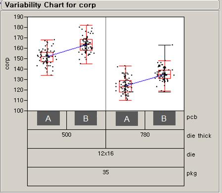
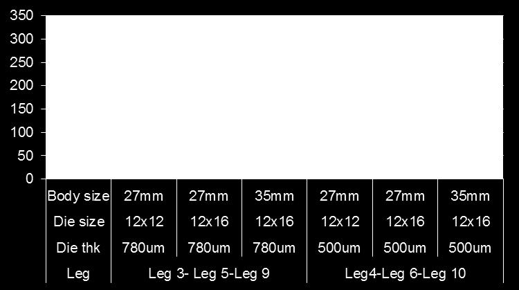
5 Figure 7. TCNCP process TCNCP process characterization is very important for each and every new product due to the different combination of die size, die thickness and Cu pillar bump layout. This is essential to avoid reliability failures induced by improper manufacturing control. Good NCP(Non-Conductive Paste) coverage can be obtained by optimum NCP dispense pattern, volume, and bonding time and force. Visual inspection for checking the coverage and fillet height along die edge will be the first step. CSAM (Confocal Scanning Acoustic Microscopy) and/or X-ray is a non-destructive way for inspecting NCP voids, while p- lap (parallel lapping) is a destructive test method. Good alignment of the Cu pillar bonding on the substrate trace is another important item, which can be checked through x-ray inspection. Often, cross-sectioning at each corner of the dies is used for validating the off-set bonding. Lastly, checking solder wetting between the Cu pillar and substrate trace is the most critical step in the characterization. Cross-section is one of the methods for checking the solder wetting condition. Resistance measurement by electrical test prior to cross-sectioning would be the ideal way to locate any bonding has micro-cracking or discontinuity issues Package Warpage and Coplanarity Figure 8. Example of NCP Dispense pattern, NCP coverage, NCP Fillet Height Because the test vehicle packages are as large as 27mm and 35mm, it is important to understand the behavior of the package warpage and BGA coplanarity. Bare-die FCBGA package warpage and BGA coplanarity data show significant impact from body size and die thickness (Tables 3 and 4) Table 3. BGA coplanarity per body size and die size/thickness Table 4. Bare-die FCBGA Package Warpage trend
 tests were performed for each readout point, time=0 and 200/500/1000/1500 hours/cycles.")
6 Reliability Tests All test vehicles were subjected to the reliability stress tests per JEDEC Standards, as listed in Table 5. Besides, electrical Open/Short tests, SAM (Scanning Acoustic Microscopy) tests were performed for each readout point, time=0 and 200/500/1000/1500 hours/cycles. Table 5 Reliability test items and conditions 4. Findings and Lessons Learned 4.1 Substrate Design Surface Finish Electrolytic Sn or Ni/Au plating are common surface finish technologies that have been qualified and being applied for HVM BOT packaging. However, these technologies could be good for the packaging using strip format substrates with wider bump pitch (i.e. larger than 50um inline), but are not suitable for the single unit format packages with high density design (i.e. less than 50um bump pitch) due to tight DR (design rules) and cost. Alternatively, electro-less plating technology becomes a more cost effective solution for the devices requiring fine bump pitch TCNCP and BOT. Hence, we have evaluated Immersion Sn, ENEPIG (Electro-less Nickel Electro-less Palladium Immersion Gold), DIG (Direct Immersion Gold), and Solder Coat surface finishes as shown in Figures 5 and Substrate Structure As it was already explained in Section-3 Design Enablement, there are many challenges on the design and layout of the substrate for TCNCP applications. Trench pattern solder resist opening is one of a common techniques which can accommodate larger number of IOs by utilizing limited space effectively. This pattern is shown in Figure 9.
7 Area Array Flip Chip Design Fine Pitch Perimeter Flip Chip Figure 9. Trench Pattern Solder Resist Opening for BOT of fine pitch perimeter micro-bumps 4.2 Findings-1: Open failure from Immersion Sn plated test vehicle Very obvious failures that we observed were open failures occurring at the interface between the Cu-pillar and BOT trace. The failure might be initiated from the Level-3 MRT (Moisture Resistance Test), and propagated further during temperature cycling (Figure 10). Most of failed pins are located on the middle row at the peripheral site. Larger body (35x35mm) and Thicker Die (780um) yielded higher open failures than smaller body (27x27mm) and thinner die (500um). Figure 10. FA of open failure at 500 cycles TCB(Temperature Cycle, Condition B ) of opens failures Figure 11. Commonality of location Figure 11 explains that die tilt might cause an insufficient solder joint at time zero and resulted in open failures after thermal cycling. Figure 12 shows Cu undercut is prone to happen in the middle row of the trace, which might be proportioned to the plating time and/or length of Cu pad Lessons learned Figure 12. Cross section of Cu undercut Use of Immersion Sn as a surface finish for fine pitch device substrates has higher risks in micro-joint open failures due to Cu undercut and the insufficient amount of solder volume for the bump to trace joint. Major differences in Electrolytic Sn plating and Electroless Immersion Sn plating are the thickness control per the plating method. Electrolytic Sn plating is an additive plating, so the thickness can be added over 3um without impacting Cu, while electroless immersion Sn plating is a chemical substitution plating which replaces Cu. Therefore, thicker Sn plating thicknesses in Immersion Sn plating means there is more Cu undercut, which will result in more solder consumption in the micro-joint system, which end up yielding non-wetting (open failures) during thermal cycling.
 adhesion.")
8 4.3 Finding-2: Open failure from ENEPIG with Flat-Plug structure Flat Plug structure This is the structure where the SR (solder resist) is coated on the pad (trace) side-walls and plugs gaps between pads (traces). This technology is beneficial in helping to prevent Cu undercut, excess electroless plating, NCP trapped voids during the TCNCP process, and reinforcement of pad (trace) adhesion. The structure and advantages of Flat-Plug are shown in Figure 13-a and 13-b. Figure 13-a. Cross-section and Structure of ENEPIG with Flat-Plug Figure 13-b. Advantages of Flat-Plug Structure Mechanism of solder outflow on ENEPIG Even with the use of the Flat-Plug structure with ENEPIG plating, we observed another obvious open failure during HTS (high temp storage). The open in the micro-joint happened due to the solder outflow over the ENEPIG surface, which results in insufficient solder. It was confirmed that the solder outflow is in proportion to the area of the ENEPIG bump landing pad. Figure 14 illustrates the mechanism of the open failure. Figure 14-a: Progress of solder outflow during MRT (Moisture Resistance Test) and HTS (High Temperature Storage) Figure 14-b: Solder outflow per landing pad area (ENEPIG)

9 4.3.3 Lessons learned Changing the surface finish from Immersion Sn to ENEPIG for the Cu-bump bond on the trace was very effective. However, we have learned that the total area of the bump landing pad should be limited within some range because the excellent wettability of ENEPIG with solder will consume an extra amount of solder. 4.4 DIG and Solder Coat Both DIG (Direct Immersion Gold) and solder coat surface finishes have demonstrated good wetting with SnAg solder of the Cu bump without Cu undercut. Though these two surface finish methods demonstrated good micro-joint interconnection and passed reliability tests, these options are yet to be favored for production due to the limited supply chain and being less cost competitive. The interconnection quality of post 500TCB (Temperature Cycle Condition B ) is shown in Figure 15. Figure 15. Cross-section of post 500TCB for DIG and Solder coat 4.5 Finding-3: ENEPIG on isro pad with Flat plug structure Based on the lessons learned from multiple DOEs, it has been realized that the area of the bump landing pad for BOT will need to be kept as small as possible to minimize the solder outflow. Figure 16 is an innovative practice of structuring isolate solder resist opening (isro) with the Flat plug structure. The benefits of the isro with Flat Plug are not allowing Cu undercut but limiting the very small amount of solder outspreading. The structure of isro with Flat-plug is shown in Figure 16. Figure 16. Design of isro BOT with Flat-plug We have been able to demonstrate the robustness of the isro with Flat-plug structure in both TCNCP manufacturability as well as the long term CPI (Chip Package Interaction) reliability. The test vehicles used for the company technology qualification have passed 2000 cycles TCB (Temperature Cycle Condition B ) and 1000 hours HTS and 96 hours uhast (unbiased-hast) with no failures so far. The actual cross-section of post 2000TCB (Temperature Cycle Condition B ) is shown in Figure 17. Figure 18 shows the actual images of the Cu-bumps on chip and substrate top metal layers of the test vehicles evaluated.


10 Figure 17. Cross-section of post 2000TCB bond of isro-flat Plug Figure 18. Actual substrate layer and Bump of the product SFF test vehicle 5. Conclusions The comprehensive development work has successfully demonstrated the robustness of manufacturability and reliability of Cu-pillar micro-bumps and TCNCP using isro with Flat-plug structure substrates. A few additional engineering validations will be able to support even larger die (400mm 2 ) and larger body size FCBGA packages. All the learning from these series of experiments can help to identify a cost effective packaging solution where fine pitch Cu-pillar bump is necessary, too. Finally, the technology has been applied for the successful launching of the company products. Additionally, this technology becomes a platform interconnection technology for cost effective advanced packaging (i.e. 2.1D and F2F), where high density micro-joint interconnection is required. 6. ACKNOWLEDGMENTS This research was conducted over a two year long intensive engineering collaboration effort among Amkor R&D, NTK, and Altera Package R&D groups. Special thanks go to the Amkor Korea R&D team, and NTK Co., Ltd. 7. REFERENCES [1] Yang-Gyoo Jung, Myung-June (MJ) Lee et al, Development of Large Die Fine Pitch Flip Chip BGA Using TCNCP Technology Electronic Components and Technology Conference, San Diego, CA, May [2] JEDEC Solid State Technology Association. JESD22-A104D, Thermal Cycling.
 Lee (mjlee@altera.com) Package Technologies R&D, Altera Corp. Mar.")
11 Packaging Technology and Design Challenges for Fine Pitch micro-bump Cu-Pillar and BOT using TCNCP Process MJ (Myung-June) Lee Package Technologies R&D, Altera Corp. Mar. 2014
12 Outline: 1. Introduction 2. Package structure, Bumping and Assembly Process Flow 3. Packaging Experimentation 3.1 Test Vehicles, Variables 3.2 Assembly (TCNCP) 3.3 Reliability Tests 4. Findings and Lessons learned 5. Conclusions
13 Introduction: Cu pillar bump enables finer bump pitch <150µ ~ 20µ Benefits of Cu bump over Solder bump : Bump joint fatigue reliability Electrical and Thermal performance Finer pitch scaling capability Environmental friendly RoHS6 Manufacturing Yield Enables small form factor (SFF) package by replacing wire bond interconnection with BOT using TCNCP: Challenges on packaging structure, design, and process engineering

14 Structure of Flip Chip Packages Molded FCBGA Typical FCBGA Fine Pitch Cu Pillar fccsp Lidless FCBGA Molded fccsp


15 Process Flow of RDL/Bump Wafer incoming PI 1 Layer RDL(Seed) deposition RDL Template photo RDL plating RDL Template strip RDL(Seed) etch PI 2 Layer UBM deposition Solder Template photo Ni/Solder plating Solder Template strip UBM etch Reflow & Clean (Animation courtesy : Amkor)


16 Process Flow of Cu Bump 1. UBM Sputter TiW/Cu 2. Template Photo 3. Cu Pillar / Solder Plating Template Photo 4. Template PR Strip 5. UBM Etching 6. Reflow (Courtesy : Amkor)
17 Process Flow of TCNCP NCP writing flip chip bonding heating MRCUF TCNCP C/A with Fluxing Pb free Reflow Flux cleaning PCB prebake PCB prebake Plasma TCNCP NCP cure Plasma Underfill Underfill cure Back-end (Courtesy : Amkor)
18 Packaging Experimentation Test Vehicles, Variables Understand baseline


19 Packaging Experimentation Test Vehicles, Variables Define objectives/deliverables prior to setting boundary condition and matrix Circular (30um) Circular (30um) Thicker Sn Cap (Immersion Tin) 12x16mmm DC 10X10 Full Loop Oval (20x45um) Oval (20x45um) Thinner Sn Cap (Immersion Tin)
20 Packaging Experimentation TCNCP assembly (Thermal Compression and Non-conductive Paste) Process optimization per die size, thickness, bump pattern Input: Bonding time/force/temp, NCP volume/pattern Output: Die placement, NCP coverage/void thru CSAM/X-ray, P- lap, X-section, Electrical continuity for open failure


21 Packaging Experimentation Package Warpage and Coplanarity Depend on Die/Package ratio, Die size, Die thickness, Core
22 Packaging Experimentation Reliability Test items and conditions
 cost")

23 Packaging Experimentation Substrate Surface finish Electrolytic Sn, thin Ni/Au lower density >50µ, strip format Electroless Platings (Immersion Sn, ENEPIG, DiG, Solder coat) cost effective for higher density >50µ, single unit format Substrate Design Trench pattern solder resist opening for effective real estate Fine Pitch Perimeter Flip Chip Area Array Flip Chip Design RDL
24 Findings and Lessons learned 1 Immersion Sn for <50µ fine pitch devices Not enough solder volume o Limited Cu column diameter to plate larger volume of solder o o Electrolytic Sn (additive) VS. Electroless Sn (chemical substitution) Cu undercut by immersion Sn Open failure at 500 TCB Cross section of Sn undercut Commonality of location of open failures
25 Findings and Lessons learned 2 Flat-Plug SR with ENEPIG Solder outflow at HTS proportion to the ENEPIG surface Progress of solder outflow over MRT and HTS Solder outflow per landing pad area (ENEPIG)
26 Findings and Lessons learned 3 ENEPIG on isro with Flat-Plug SR No Cu undercut Less amount of solder outspreading Demonstrated HVM processable manufacturability and reliability Passed all reliability tests TCB, HTS, unbiased-hast Design of isro BOT with Flat-plug X-section of post 2000TCB parts


27 Acknowledgement Author would like to recognize over 2 years long full dedication and intensive engineering collaboration of Amkor R&D, NTK R&D and Manufacturing team, Altera Package R&D.
Packaging Technology and Design Challenges for Fine Pitch Cu Pillar and BOT (Bond on Trace) using Thermal Compression Bonding
 using Thermal Compression Bonding") Packaging Technology and Design Challenges for Fine Pitch Cu Pillar and BOT (Bond on Trace) using Thermal Compression Bonding MJ (Myung-June) Lee 1, Chew Ching Lim 2, Pheak Ti Teh 2 1: Altera Corporation,
Packaging Technology and Design Challenges for Fine Pitch Cu Pillar and BOT (Bond on Trace) using Thermal Compression Bonding MJ (Myung-June) Lee 1, Chew Ching Lim 2, Pheak Ti Teh 2 1: Altera Corporation,
POSSUM TM Die Design as a Low Cost 3D Packaging Alternative
 POSSUM TM Die Design as a Low Cost 3D Packaging Alternative The trend toward 3D system integration in a small form factor has accelerated even more with the introduction of smartphones and tablets. Integration
Fine Pitch Cu Pillar Assembly Challenges for Advanced Flip Chip Package
 Fine Pitch Cu Pillar Assembly Challenges for Advanced Flip Chip Package by Nokibul Islam and Vinayak Pandey, STATS ChipPAC, Inc. Ming-Che Hsieh, STATS ChipPAC Pte. Ltd. Kang Keon Taek, STATS ChipPAC Korea
10nm CPI Study for Fine Pitch Flip Chip Attach Process and Substrate
 10nm CPI Study for Fine Pitch Flip Chip Attach Process and Substrate Ming-Che Hsieh, Chi-Yuan Chen*, Ian Hsu*, Stanley Lin* and KeonTaek Kang** Product and Technology Marketing / STATS ChipPAC Pte. Ltd.
SOLDERABLE ANISOTROPIC CONDUCTIVE ADHESIVES FOR 3D PACKAGE APPLICATIONS
 SOLDERABLE ANISOTROPIC CONDUCTIVE ADHESIVES FOR 3D PACKAGE APPLICATIONS ABSTRACT: Dr. Mary Liu and Dr. Wusheng Yin YINCAE Advanced Materials, LLC Albany, NY 3D packaging has recently become very attractive
B. Flip-Chip Technology
 B. Flip-Chip Technology B1. Level 1. Introduction to Flip-Chip techniques B1.1 Why flip-chip? In the development of packaging of electronics the aim is to lower cost, increase the packaging density, improve
The Future of Packaging ~ Advanced System Integration
 The Future of Packaging ~ Advanced System Integration Enabling a Microelectronic World R. Huemoeller SVP, Adv. Product / Platform Develop June 2013 Product Segments End Market % Share Summary 2 New Product
Min Tao, Ph. D, Ashok Prabhu, Akash Agrawal, Ilyas Mohammed, Ph. D, Bel Haba, Ph. D Oct , IWLPC
 PACKAGE-ON-PACKAGE INTERCONNECT FOR FAN-OUT WAFER LEVEL PACKAGES Min Tao, Ph. D, Ashok Prabhu, Akash Agrawal, Ilyas Mohammed, Ph. D, Bel Haba, Ph. D Oct 18-20 2016, IWLPC 1 Outline Laminate to Fan-Out
Application Note AN-1011
 AN-1011 Board Mounting Application Note for 0.800mm Pitch Devices For part numbers IRF6100, IRF6100PBF, IR130CSP, IR130CSPPBF, IR140CSP, IR140CSPPBF, IR1H40CSP, IR1H40CSPPBF By Hazel Schofield and Philip
BOARD DESIGN, SURFACE MOUNT ASSEMBLY AND BOARD LEVEL RELIABILITY ASPECTS OF FUSIONQUAD TM PACKAGES
 BOARD DESIGN, SURFACE MOUNT ASSEMBLY AND BOARD LEVEL RELIABILITY ASPECTS OF FUSIONQUAD TM PACKAGES Ahmer Syed 1, Sundar Sethuraman 2, WonJoon Kang 1, Gary Hamming 1, YeonHo Choi 1 1 Amkor Technology, Inc.
2.5D Platform (Examples of products produced to date are shown here to demonstrate Amkor's production capabilities)
") Wafer Finishing & Flip Chip Stacking interconnects have emerged to serve a wide range of 2.5D- & 3D- packaging applications and architectures that demand very high performance and functionality at the
Wafer Finishing & Flip Chip Stacking interconnects have emerged to serve a wide range of 2.5D- & 3D- packaging applications and architectures that demand very high performance and functionality at the
3D TSV Micro Cu Column Chip-to-Substrate/Chip Assmbly/Packaging Technology
 3D TSV Micro Cu Column Chip-to-Substrate/Chip Assmbly/Packaging Technology by Seung Wook Yoon, *K. T. Kang, W. K. Choi, * H. T. Lee, Andy C. B. Yong and Pandi C. Marimuthu STATS ChipPAC LTD, 5 Yishun Street
MICROELECTRONICS ASSSEMBLY TECHNOLOGIES. The QFN Platform as a Chip Packaging Foundation
 West Coast Luncheon January 15, 2014. PROMEX PROMEX INDUSTRIES INC. MICROELECTRONICS ASSSEMBLY TECHNOLOGIES The QFN Platform as a Chip Packaging Foundation 3075 Oakmead Village Drive Santa Clara CA Ɩ 95051
Advanced Embedded Packaging for Power Devices
 2017 IEEE 67th Electronic Components and Technology Conference Advanced Embedded Packaging for Power Devices Naoki Hayashi, Miki Nakashima, Hiroshi Demachi, Shingo Nakamura, Tomoshige Chikai, Yukari Imaizumi,
Application Note 5026
 Surface Laminar Circuit (SLC) Ball Grid Array (BGA) Eutectic Surface Mount Assembly Application Note 5026 Introduction This document outlines the design and assembly guidelines for surface laminar circuitry
Data Sheet _ R&D. Rev Date: 8/17
 Data Sheet _ R&D Rev Date: 8/17 Micro Bump In coming years the interconnect density for several applications such as micro display, imaging devices will approach the pitch 10um and below. Many research
Introduction of IMS Technology for Advanced Solder Bumping on Wafers / Laminates
 Introduction of IMS Technology for Advanced Solder Bumping on Wafers / Laminates Science & Technology IBM Research Tokyo Yasumitsu Orii, PhD Senju Metal Industry Co.,TW Deputy General Manager Lewis Huang
Advances in stacked-die packaging
 pg.10-15-carson-art 16/6/03 4:12 pm Page 1 The stacking of die within IC packages, primarily Chip Scale Packages (CSP) Ball Grid Arrays (BGAs) has evolved rapidly over the last few years. The now standard
AN5046 Application note
 Application note Printed circuit board assembly recommendations for STMicroelectronics PowerFLAT packages Introduction The PowerFLAT package (5x6) was created to allow a larger die to fit in a standard
Innovations Push Package-on-Package Into New Markets. Flynn Carson. STATS ChipPAC Inc Kato Rd Fremont, CA 94538
 Innovations Push Package-on-Package Into New Markets by Flynn Carson STATS ChipPAC Inc. 47400 Kato Rd Fremont, CA 94538 Copyright 2010. Reprinted from Semiconductor International, April 2010. By choosing
Study on Solder Joint Reliability of Fine Pitch CSP
 As originally published in the IPC APEX EXPO Conference Proceedings. Study on Solder Joint Reliability of Fine Pitch CSP Yong (Hill) Liang, Hank Mao, YongGang Yan, Jindong (King) Lee. AEG, Flextronics
Automotive Devices: Quad No- Lead (QFN) Technology with Inspectable Solder Connections
 Technology with Inspectable Solder Connections") Automotive Devices: Quad No- Lead (QFN) Technology with Inspectable Solder Connections FTF-SDS-F0026 Dwight Daniels Package Engineer A P R. 2 0 1 4 TM External Use Agenda Wettable Lead Ends / Definition
Automotive Devices: Quad No- Lead (QFN) Technology with Inspectable Solder Connections FTF-SDS-F0026 Dwight Daniels Package Engineer A P R. 2 0 1 4 TM External Use Agenda Wettable Lead Ends / Definition
Challenges of Evolving Technology in the Workplace. Tips. Bubba Powers. Board Density. Best Rework Soldering Practices. Power. Substrates.
 Real Estate Finishes Power Component Technology Board Density Tips Challenges of Evolving Technology in the Workplace Substrates Component Size Bubba Powers Manager of Technical Services Weller North America
APPLICATION NOTE 6381 ORGANIC LAND GRID ARRAY (OLGA) AND ITS APPLICATIONS
 AND ITS APPLICATIONS") Keywords: OLGA, SMT, PCB design APPLICATION NOTE 6381 ORGANIC LAND GRID ARRAY (OLGA) AND ITS APPLICATIONS Abstract: This application note discusses Maxim Integrated s OLGA and provides the PCB design and
Keywords: OLGA, SMT, PCB design APPLICATION NOTE 6381 ORGANIC LAND GRID ARRAY (OLGA) AND ITS APPLICATIONS Abstract: This application note discusses Maxim Integrated s OLGA and provides the PCB design and
Silicon Interposers enable high performance capacitors
 Interposers between ICs and package substrates that contain thin film capacitors have been used previously in order to improve circuit performance. However, with the interconnect inductance due to wire
Flip Chips. FA10-200x200 FA10-400x400 FA10-600x x 200 mils 400 x 400 mils
 Flip Chip FlipChip International Flip Chip describes the method of electrically connecting the die to the package carrier. The package carrier, either substrate or leadframe, then provides the connection
Capabilities of Flip Chip Defects Inspection Method by Using Laser Techniques
 Capabilities of Flip Chip Defects Inspection Method by Using Laser Techniques Sheng Liu and I. Charles Ume* School of Mechanical Engineering Georgia Institute of Technology Atlanta, Georgia 3332 (44) 894-7411(P)
The Role of Flip Chip Bonding in Advanced Packaging David Pedder
 The Role of Flip Chip Bonding in Advanced Packaging David Pedder David Pedder Associates Stanford in the Vale Faringdon Oxfordshire The Role of Flip Chip Bonding in Advanced Packaging Outline Flip Chip
Organic Packaging Substrate Workshop Overview
 Organic Packaging Substrate Workshop Overview Organized by: International Electronics Manufacturing Initiative (inemi) Mario A. Bolanos November 17-18, 2009 1 Organic Packaging Substrate Workshop Work
Specifications subject to change Packaging
 VCSEL Standard Product Packaging Options All standard products are represented in the table below. The Part Number for a standard product is determined by replacing the x in the column Generic Part Number
TOLERANCE FORGOTTEN: IMPACTS OF TODAY S COMPONENT PACKAGING AND COPPER ROUTING ON ELECTRONIC
 TOLERANCE FORGOTTEN: IMPACTS OF TODAY S COMPONENT PACKAGING AND COPPER ROUTING ON ELECTRONIC Presented By: Dale Lee E-mail: Dale.Lee@Plexus.Com April 2013 High Layer Counts Wide Range Of Component Package
Broadband Printing: The New SMT Challenge
 Broadband Printing: The New SMT Challenge Rita Mohanty & Vatsal Shah, Speedline Technologies, Franklin, MA Gary Nicholls, Ron Tripp, Cookson Electronic Assembly Materials Engineered Products, Johnson City,
Electroless Bumping for 300mm Wafers
 Electroless Bumping for 300mm Wafers T. Oppert Internepcon 2006 Tokyo Big Sight, Japan Outline Short Company Profile Electroless Ni/Au Under Bump Metallization UBM for Copper Devices Solder Bumping: Stencil
Getting the FLI Lead Out. Thomas J. De Bonis Assembly & Test Technology Development Technology and Manufacturing Group
 Getting the FLI Lead Out Thomas J. De Bonis Assembly & Test Technology Development Technology and Manufacturing Group Lead has been used in flip chip FLI for decades. RoHS Exemption 15 was enacted in recognition
AND8081/D. Flip Chip CSP Packages APPLICATION NOTE
 Flip Chip CSP Packages Prepared by: Denise Thienpont ON Semiconductor Staff Engineer APPLICATION NOTE Introduction to Chip Scale Packaging This application note provides guidelines for the use of Chip
Bob Willis Process Guides
 What is a Printed Circuit Board Pad? What is a printed circuit board pad, it may sound like a dumb question but do you stop to think what it really does and how its size is defined and why? A printed circuit
Chapter 2. Literature Review
 Chapter 2 Literature Review 2.1 Development of Electronic Packaging Electronic Packaging is to assemble an integrated circuit device with specific function and to connect with other electronic devices.
mcube WLCSP Application Note
 AN-002 Rev.02 mcube WLCSP Application Note AN-002 Rev.02 mcube, Inc. 1 / 20 AN-002 Rev.02 Guidelines for Printed Circuit Board (PCB) Design and Assembly with mcube Wafer Level Chip Scale Package (WLCSP)
TCLAD: TOOLS FOR AN OPTIMAL DESIGN
 TCLAD: TOOLS FOR AN OPTIMAL DESIGN THINGS TO CONSIDER WHEN DESIGNING CIRCUITS Many factors come into play in circuit design with respect to etching, surface finishing and mechanical fabrication processes;
Two major features of this text
 Two major features of this text Since explanatory materials are systematically made based on subject examination questions, preparation
What the Designer needs to know
 White Paper on soldering QFN packages to electronic assemblies. Brian J. Leach VP of Sales and Marketing AccuSpec Electronics, LLC Defect free QFN Assembly What the Designer needs to know QFN Description:
Interconnection Challenge in Wire Bonding Ag alloy wire. Jensen Tsai / 蔡瀛洲, SPIL, Taiwan
 1 Interconnection Challenge in Wire Bonding Ag alloy wire Jensen Tsai / 蔡瀛洲, SPIL, Taiwan 2 Content Ag Alloy Wire Type Market Ag Alloy Wire Benefits Workability and Reliability Performance IMC behavior
An Introduction to Electronics Systems Packaging. Prof. G. V. Mahesh. Department of Electronic Systems Engineering
 An Introduction to Electronics Systems Packaging Prof. G. V. Mahesh Department of Electronic Systems Engineering India Institute of Science, Bangalore Module No. # 02 Lecture No. # 08 Wafer Packaging Packaging
Advanced Packaging - Pulsed-laser Heating for Flip Chip Assembly
 Page 1 of 5 Pulsed-laser Heating for Flip Chip Assembly A stress-free alternative By Thorsten Teutsch, Ph.D., Pac Tech USA, Elke Zakel, Ph.D., and Ghassem Azdasht, Pac Tech GmbH As flip chip applications
Laminate Based Fan-Out Embedded Die Technologies: The Other Option
 Laminate Based Fan-Out Embedded Die Technologies: The Other Option Theodore (Ted) G. Tessier, Tanja Karila*, Tuomas Waris*, Mark Dhaenens and David Clark FlipChip International, LLC 3701 E University Drive
Chapter 11 Testing, Assembly, and Packaging
 Chapter 11 Testing, Assembly, and Packaging Professor Paul K. Chu Testing The finished wafer is put on a holder and aligned for testing under a microscope Each chip on the wafer is inspected by a multiple-point
Processes for Flexible Electronic Systems
 Processes for Flexible Electronic Systems Michael Feil Fraunhofer Institut feil@izm-m.fraunhofer.de Outline Introduction Single sheet versus reel-to-reel (R2R) Substrate materials R2R printing processes
Peripheral Flip Chip Interconnection on Au Plated Pads using Solder-Capped Cu Pillar Bumps
 Noma et al.: Peripheral Flip Chip Interconnection on Au (1/6) [Technical Paper] Peripheral Flip Chip Interconnection on Au Plated Pads using Solder-Capped Cu Pillar Bumps Hirokazu Noma*, Kazushige Toriyama*,
!"#$%&'()'*"+,+$&#' ' '
'*+,+$&#' ' '") !"#$%&'()'*"+,+$&#' *"89"+&+6'B22&83%45'8/6&10/%2'A"1'/22&83%4'/+#'C"0+0+D'8&67"#2'0+'&%&
!"#$%&'()'*"+,+$&#' *"89"+&+6'B22&83%45'8/6&10/%2'A"1'/22&83%4'/+#'C"0+0+D'8&67"#2'0+'&%&
Flexline - A Flexible Manufacturing Method for Wafer Level Packages (Extended Abstract)
") Flexline - A Flexible Manufacturing Method for Wafer Level Packages (Extended Abstract) by Tom Strothmann, *Damien Pricolo, **Seung Wook Yoon, **Yaojian Lin STATS ChipPAC Inc.1711 W Greentree Drive Tempe,
Flexline - A Flexible Manufacturing Method for Wafer Level Packages (Extended Abstract) by Tom Strothmann, *Damien Pricolo, **Seung Wook Yoon, **Yaojian Lin STATS ChipPAC Inc.1711 W Greentree Drive Tempe,
New Approaches to Develop a Scalable 3D IC Assembly Method
 New Approaches to Develop a Scalable 3D IC Assembly Method Charles G. Woychik Ph.D. Sangil Lee, Ph.D., Scott McGrath, Eric Tosaya and Sitaram Arkalgud Ph.D. Invensas Corporation 3025 Orchard Parkway San
IMPROVED SMT AND BLR OF 0.35MM PITCH WAFER LEVEL PACKAGES
 As originally published in the SMTA Proceedings. IMPROVED SMT AND BLR OF 0.35MM PITCH WAFER LEVEL PACKAGES Brian Roggeman and Beth Keser Qualcomm Technologies, Inc. San Diego, CA, USA roggeman@qti.qualcomm.com
FLIP CHIP LED SOLDER ASSEMBLY
 As originally published in the SMTA Proceedings FLIP CHIP LED SOLDER ASSEMBLY Gyan Dutt, Srinath Himanshu, Nicholas Herrick, Amit Patel and Ranjit Pandher, Ph.D. Alpha Assembly Solutions South Plainfield,
SESUB - Its Leadership In Embedded Die Packaging Technology
 SESUB - Its Leadership In Embedded Die Packaging Technology Sip Conference China 2018 TDK Corporation ECBC, PAF, SESUB BU Kofu, Japan October 17, 2018 Contents SESUB Introduction SESUB Process SESUB Quality
Flip Chip Assembly on PCB Substrates with Coined Solder Bumps
 Flip Chip Assembly on PCB Substrates with Coined Solder Bumps Jae-Woong Nah, Kyung W. Paik, Soon-Jin Cho*, and Won-Hoe Kim* Department of Materials Sci. & Eng., Korea Advanced Institute of Science and
TN016. PCB Design Guidelines for 5x5 DFN Sensors. Introduction. Package Marking
 PCB Design Guidelines for 5x5 DFN Sensors Introduction This technical note is intended to provide information about Kionix s 5 x 5 mm DFN (non wettable flank, i.e. standard) packages and guidelines for
BGA (Ball Grid Array)
") BGA (Ball Grid Array) National Semiconductor Application Note 1126 November 2002 Table of Contents Introduction... 2 Package Overview... 3 PBGA (PLASTIC BGA) CONSTRUCTION... 3 TE-PBGA (THERMALLY ENHANCED
BGA (Ball Grid Array) National Semiconductor Application Note 1126 November 2002 Table of Contents Introduction... 2 Package Overview... 3 PBGA (PLASTIC BGA) CONSTRUCTION... 3 TE-PBGA (THERMALLY ENHANCED
ACOUSTIC MICRO IMAGING ANALYSIS METHODS FOR 3D PACKAGES
 ACOUSTIC MICRO IMAGING ANALYSIS METHODS FOR 3D PACKAGES Janet E. Semmens Sonoscan, Inc. Elk Grove Village, IL, USA Jsemmens@sonoscan.com ABSTRACT Earlier studies concerning evaluation of stacked die packages
Hermetic Packaging Solutions using Borosilicate Glass Thin Films. Lithoglas Hermetic Packaging Solutions using Borosilicate Glass Thin Films
 Hermetic Packaging Solutions using Borosilicate Glass Thin Films 1 Company Profile Company founded in 2006 ISO 9001:2008 qualified since 2011 Headquarters and Production in Dresden, Germany Production
The Design Challenge to Integrate High Performance Organic Packaging into High End ASIC Strategic Space Based Applications.
 The Design Challenge to Integrate High Performance Organic Packaging into High End ASIC Strategic Space Based Applications May 8, 2007 Abstract: The challenge to integrate high-end, build-up organic packaging
Selecting Stencil Technologies to Optimize Print Performance
 As originally published in the IPC APEX EXPO Conference Proceedings. Selecting Stencil Technologies to Optimize Print Performance Chrys Shea Shea Engineering Services Burlington, NJ USA Abstract The SMT
Advanced High-Density Interconnection Technology
 Advanced High-Density Interconnection Technology Osamu Nakao 1 This report introduces Fujikura s all-polyimide IVH (interstitial Via Hole)-multi-layer circuit boards and device-embedding technology. Employing
Michael R. Creeden CEO/CID+ San Diego PCB, Inc. & EPTAC (858)
") Michael R. Creeden CEO/CID+ San Diego PCB, Inc. & EPTAC mike.creeden@sdpcb.com (858)271-5722 1. Why we collaborate? 2. When do we collaborate? 3. Who do we collaborate with? 4. What do we collaborate?
Michael R. Creeden CEO/CID+ San Diego PCB, Inc. & EPTAC mike.creeden@sdpcb.com (858)271-5722 1. Why we collaborate? 2. When do we collaborate? 3. Who do we collaborate with? 4. What do we collaborate?
Innovative Embedded Technologies to Enable Thinner IoT/Wearable/Mobile Devices
 Innovative Embedded Technologies to Enable Thinner IoT/Wearable/Mobile Devices Jensen Tsai Deputy Director, SPIL Building a Smarter World Wearable Internet of Things Building a Smarter World Mobile Devices
2016 Substrate & Package Technology Workshop Highlight
 2016 Substrate & Package Technology Workshop Highlight Webinar July 13, 2016 Theme of the Workshop inemi roadmap and Technical plan highlighted that year 2015 was the year entering critical package technology
The 3D Silicon Leader
 The 3D Silicon Leader 3D Silicon IPD for smaller and more reliable Implantable Medical Devices ATW on Advanced Packaging for Wireless Medical Devices Mohamed Mehdi Jatlaoui, Sébastien Leruez, Olivier Gaborieau,
Bumping of Silicon Wafers using Enclosed Printhead
 Bumping of Silicon Wafers using Enclosed Printhead By James H. Adriance Universal Instruments Corp. SMT Laboratory By Mark A. Whitmore DEK Screen Printers Advanced Technologies Introduction The technology
Transistor Installation Instructions
 INTRODUCTION When inserting high power RF transistor packages into amplifier circuits there are two important objectives. Firstly, removing heat and, secondly, providing a longterm reliable solder joint
Thermal Cycling and Fatigue
 Thermal Cycling and Fatigue Gil Sharon Introduction The majority of electronic failures are thermo-mechanically related by thermally induced stresses and strains. The excessive difference in coefficients
TSV MEOL (Mid-End-Of-Line) and its Assembly/Packaging Technology for 3D/2.5D Solutions
 and its Assembly/Packaging Technology for 3D/2.5D Solutions") TSV MEOL (Mid-End-Of-Line) and its Assembly/Packaging Technology for 3D/2.5D Solutions Seung Wook YOON, D.J. Na, *K. T. Kang, W. K. Choi, C.B. Yong, *Y.C. Kim and Pandi C. Marimuthu STATS ChipPAC Ltd.
TSV MEOL (Mid-End-Of-Line) and its Assembly/Packaging Technology for 3D/2.5D Solutions Seung Wook YOON, D.J. Na, *K. T. Kang, W. K. Choi, C.B. Yong, *Y.C. Kim and Pandi C. Marimuthu STATS ChipPAC Ltd.
Fan-Out Solutions: Today, Tomorrow the Future Ron Huemoeller
 Fan-Out Solutions: Today, Tomorrow the Future Ron Huemoeller Corporate Vice President, WW RnD & Technology Strategy 1 In the Beginning ewlb 2 Fan Out Packaging Emerges Introduction of Fan Out (ewlb) Marketed
Ultra-thin Die Characterization for Stack-die Packaging
 Ultra-thin Die Characterization for Stack-die Packaging Wei Sun, W.H. Zhu, F.X. Che, C.K. Wang, Anthony Y.S. Sun and H.B. Tan United Test & Assembly Center Ltd (UTAC) Packaging Analysis & Design Center
Design and Development of True-CSP
 Design and Development of True-CSP *Kolan Ravi Kanth, Francis K.S. Poh, B.K. Lim, Desmond Y.R. Chong, Anthony Sun, H.B. Tan United Test & Assembly Center Ltd (UTAC) 5 Serangoon North Ave 5, Singapore 554916
CHAPTER 11: Testing, Assembly, and Packaging
 Chapter 11 1 CHAPTER 11: Testing, Assembly, and Packaging The previous chapters focus on the fabrication of devices in silicon or the frontend technology. Hundreds of chips can be built on a single wafer,
Assembly Instructions for SCA6x0 and SCA10x0 series
 Technical Note 71 Assembly Instructions for SCA6x0 and SCA10x0 series TABLE OF CONTENTS Table of Contents...1 1 Objective...2 2 VTI'S DIL-8 and DIL-12 packages...2 3 Package Outline and Dimensions...2
Fill the Void IV: Elimination of Inter-Via Voiding
 Fill the Void IV: Elimination of Inter-Via Voiding Tony Lentz FCT Assembly Greeley, CO, USA Greg Smith BlueRing Stencils Lumberton, NJ, USA ABSTRACT Voids are a plague to our electronics and must be eliminated!
Overcoming the Challenges of HDI Design
 ALTIUMLIVE 2018: Overcoming the Challenges of HDI Design Susy Webb Design Science Sr PCB Designer San Diego Oct, 2018 1 Challenges HDI Challenges Building the uvia structures The cost of HDI (types) boards
High Reliability and High Temperature Application Solution Solder Joint Encapsulant Paste
 High Reliability and High Temperature Application Solution Solder Joint Encapsulant Paste YINCAE Advanced Materials, LLC WHITE PAPER October 2017 2017 YINCAE Advanced Materials, LLC - All Rights Reserved.
BGA/CSP Re-balling Bob Doetzer Circuit Technology Inc.
 BGA/CSP Re-balling Bob Doetzer Circuit Technology Inc. www.circuittechnology.com The trend in the electronics interconnect industry towards Area Array Packages type packages (BGA s, CSP s, CGA s etc.)
Compression Molding. Solutions for 3D TSV and other advanced packages as well as cost savings for standard package applications
 Compression Molding Solutions for 3D TSV and other advanced packages as well as cost savings for standard package applications 1. Company Introduction 2. Package Development Trend 3. Compression FFT Molding
mcube LGA Package Application Note
 AN-001 Rev.02 mcube LGA Package Application Note AN-001 Rev.02 mcube, Inc. 1 / 21 AN-001 Rev.02 Guidelines for Printed Circuit Board (PCB) Design and Assembly with mcube Land Grid Array (LGA) Package Sensors
TAIPRO Engineering. Speaker: M. Saint-Mard Managing director. TAIlored microsystem improving your PROduct
 TAIPRO Engineering MEMS packaging is crucial for system performance and reliability Speaker: M. Saint-Mard Managing director TAIPRO ENGINEERING SA Michel Saint-Mard Administrateur délégué m.saintmard@taipro.be
"Low Cost Electroless Bumping for Ultra Fine Pitch Applications in 8" and 12" Wafers"
 1 "Low Cost Electroless Bumping for Ultra Fine Pitch Applications in 8" and 12" Wafers" Elke Zakel, Thomas Oppert, Ghassem Azdasht, Thorsten Teutsch * Pac Tech Packaging Technologies GmbH Am Schlangenhorst
(a) (d) (e) (b) (c) (f) 3D-NAND Flash and Its Manufacturing Process
 (d) (e) (b) (c) (f) 3D-NAND Flash and Its Manufacturing Process") 3D-NAND Flash and Its Manufacturing Process 79 (d) Si Si (b) (c) (e) Si (f) +1-2 (g) (h) Figure 2.33 Top-down view in cap oxide and (b) in nitride_n-2; (c) cross-section near the top of the channel; top-down
3D-NAND Flash and Its Manufacturing Process 79 (d) Si Si (b) (c) (e) Si (f) +1-2 (g) (h) Figure 2.33 Top-down view in cap oxide and (b) in nitride_n-2; (c) cross-section near the top of the channel; top-down
AN-5067 PCB Land Pattern Design and Surface Mount Guidelines for MLP Packages
 Introduction AN-5067 Fairchild Semiconductor Application Note September 2005 Revised September 2005 PCB Land Pattern Design and Surface Mount Guidelines for MLP Packages The current miniaturization trend
Assembly Instructions for SCC1XX0 series
 Technical Note 82 Assembly Instructions for SCC1XX0 series TABLE OF CONTENTS Table of Contents...1 1 Objective...2 2 VTI's 32-lead Dual In-line Package (DIL-32)...2 3 DIL-32 Package Outline and Dimensions...2
AltiumLive 2017: Creating Documentation for Successful PCB Manufacturing
 AltiumLive 2017: Creating Documentation for Successful PCB Manufacturing Julie Ellis TTM Field Applications Engineer Thomas Schneider Field Applications Engineer 1 Agenda 1 Complexity & Cost 2 3 4 5 6
QUALITY SEMICONDUCTOR, INC.
 Q QUALITY SEMICONDUCTOR, INC. AN-20 Board Assembly Techniques for 0.4mm Pin Pitch Surface Mount Packages Application Note AN-20 The need for higher performance systems continues to push both silicon and
IMAGE SENSOR EVOLUTION AND ENABLING 3D TECHNOLOGIES
 Fig. 5: Scanning Electron Microscopy images (TOP view, 3D view, Zoome including all metal levels of the BSI imager structure. (dashed line shows bonding IMAGE SENSOR EVOLUTION AND ENABLING 3D TECHNOLOGIES
The Future of Packaging and Cu Wire Bonding Advances. Ivy Qin
 The Future of Packaging and Cu Wire Bonding Advances Ivy Qin Introduction Semiconductors have been around for over 70 years Packaging is playing a more and more important role, providing low cost high
Surface Mount Header Assembly Employs Capillary Action
 New Product Technology Surface Mount Header Assembly Employs Capillary Action Zierick s unique header assembly features capillary action to improve solder joint strength. As a result, pin retention force
High Efficient Heat Dissipation on Printed Circuit Boards. Markus Wille, R&D Manager, Schoeller Electronics Systems GmbH
 High Efficient Heat Dissipation on Printed Circuit Boards Markus Wille, R&D Manager, Schoeller Electronics Systems GmbH m.wille@se-pcb.de Introduction 2 Heat Flux: Q x y Q z The substrate (insulation)
3D ICs: Recent Advances in the Industry
 3D ICs: Recent Advances in the Industry Suresh Ramalingam Senior Director, Advanced Packaging Outline 3D IC Background 3D IC Technology Development Summary Acknowledgements Stacked Silicon Interconnect
Enabling concepts: Packaging Technologies
 Enabling concepts: Packaging Technologies Ana Collado / Liam Murphy ESA / TEC-EDC 01/10/2018 ESA UNCLASSIFIED - For Official Use Enabling concepts: Packaging Technologies Drivers for the future: Higher
NEW PACKAGING AND INTERCONNECT TECHNOLOGIES FOR ULTRA THIN CHIPS
 NEW PACKAGING AND INTERCONNECT TECHNOLOGIES FOR ULTRA THIN CHIPS Christine Kallmayer and Rolf Aschenbrenner Fraunhofer IZM Berlin, Germany kallmayer@izm.fhg.de Julian Haberland and Herbert Reichl Technical
CHARACTERIZATION OF FLIP CHIP BUMP FAILURE MODES USING HIGH FREQUENCY ACOUSTIC MICRO IMAGING
 CHARACTERIZATION OF FLIP CHIP BUMP FAILURE MODES USING HIGH FREQUENCY ACOUSTIC MICRO IMAGING Janet E. Semmens and Lawrence W. Kessler SONOSCAN, INC. 530 East Green Street Bensenville, IL 60106 U.S.A. Tel:
MICROBUMP CREATION SYSTEM FOR ADVANCED PACKAGING APPLICATIONS
 MICROBUMP CREATION SYSTEM FOR ADVANCED PACKAGING APPLICATIONS Andrew Ahr, EKC Technology, & Chester E. Balut, DuPont Electronic Technologies Alan Huffman, RTI International Abstract Today, the electronics
50 Micron Pitch Flip Chip Bumping Technology: Processes and Applications
 50 Micron Pitch Flip Chip Bumping Technology: Processes and Applications Alan Huffman Center for Materials and Electronic Technologies huffman@rti.org Outline RTI Identity/History Historical development
Chemnitzer Seminar System Integration Technologies. Solder Jetting, Rework & electroless UBM Deposition
 Chemnitzer Seminar System Integration Technologies June 14 15, 2016 Solder Jetting, Rework & electroless UBM Deposition Made in Germany PacTech Group - Milestones 1995 PacTech founded in Berlin, Germany
Application Note. Soldering Guidelines for Module PCB Mounting Rev 13
 Application Note Soldering Guidelines for Module PCB Mounting Rev 13 OBJECTIVE The objective of this application note is to provide ANADIGICS customers general guidelines for PCB second level interconnect