Brief Introduction of Sigurd IC package Assembly
|
|
|
- Merilyn Allen
- 6 years ago
- Views:
Transcription

1 Brief Introduction of Sigurd IC package Assembly
2 Content Package Development Trend Product Brief Sawing type QFN Representative MEMS Product LGA Light Sensor Proximity Sensor High Yield Capability Low Cost Solution Rapid Product Design / Phase-in 2
3 Sigurd Assemblies Today Thin WLCSP QFN/DFN LGA Proximity sensor TSOP SOT/TSOT QFP SSOP MEMS Thick DIP SOP CIS/CCM PLCC Large 3 Small

4 Assembly Product Roadmap 300mm WLCSP Technology Integrate LED & Receiver Light Sensor Single receiver RF 3G technology LGA Embedded component Solar cell module MEMS G-sensor technology Glass Wafer sawing MEMS SIP assembly Jan Jan Jan Jan Development Photo type Production Direction: small size, multi-chip, more component. 4
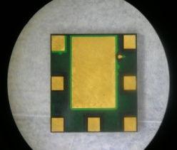
5 Package Structure Sawing type / QFN Molding Compound Chip Gold Wire Chip Mold Compound Cross section 0.55, 0.75 & 0.9 mm Lead Frame (PPF/ Spot Ag) Exposed Die pad Marking OOOOO OOOOO DA Epoxy Bottom view Top view 5

6 Package Type QFN/ DFN Remark: : L/F is ready. : L/F need to be created. Package thickness: 0.55, 0.75, and 0.90 mm 6
 CMOS Controller MEMS Die Au Bond-wire")
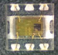
7 Representative MEMS Product MEMS Telecom Switch (production) High-volume application Stacked Die for small footprint and low impedance interconnect CMOS Controller for switch drive and digital interface Lid (LCP) CMOS Controller MEMS Die Au Bond-wire Leadframe 7


8 MEMS Stacking Die Technology Design and develop MEMS with driver in one package System in Package technology. Multi-layer bonding 4-layer wire loop capability. Package thermal expansion control solution. Package type: Injection molded type & Air cavity type. Turn key solution. Pictures of stacking die with wire bonding 8


9 Thin Package Solution - SOT / TSOT Features: 2.9x1.6mm package size 1.9mm lead pitch SOT thickness 1.1mm TSOT thickness 0.75mm Green product Application: Power management Power switch RFID 9


10 Features: LGA (land grid array) 3x3mm to 10x7mm package size 7 to 29 pin counts 0.4mm lead pitch Green finish available Excellent electrical and thermal performance Full in house design ability Passive component Application: RF module Logic Memory Epoxy Substrate Passive component 10

11 Light Sensor Features: 1.6x1.6mm to 3x3mm package size 4 to 12 pin counts 0.5mm lead pitch Green finish available Excellent electrical and light performance Full in house design ability Application: Clear Compound Chip Gold Wire Cell phone Notebook `` Clear Compound Chip Touch control panel Silver Epoxy PPF Lead Frame 11


12 Proximity Sensor Features: Customized package 4 to 12 pin counts Integrate LED and Receiver in one package Green finish available Excellent electrical and light performance Full in house design ability Application: Cell phone Notebook Touch control panel 12
13 WLCSP Chip Cover Chip Bump Carrier Features: Die size: 0.3mm x 0.3mm till 15mm x 15mm Bump size: 90 ~ 250um Carrier/Cover tape: 8/12/16/24/32 mm tape width capability waffle pack: 2 x 2 ~ 4 x
14 High yield capability Ass y y Yield trend: Assembly Yield 100 Total Yield 99.5 Power QFN 99 Jan' 10 Feb' 10 Mar' 10 Apr' 10 May' 10 Jun ' 10 July ' 10 Aug '10 Sep '10 Oct '10 Nov '10 Dec '10 Jan '11 Feb '11 Mar. '11 Apr '11 May '11 Jun. '11 LGA Total Power QFN LGA Month Remark: average yield above 99.95%. 14
15 Equipment List For Assembly Process Vendor Remark Grinding Okamoto Accuracy: +/- 5um Saw Disco/TSC Die Bond ESEC / ASM / Panasonic Accuracy: +/- 25um Wire Bond ASM / KNS / Panasonic Accuracy: +/- 3um Sealing RJR / GPM Molding Towa / Ki-Giant Offset: +/- 20um Marking Singulation saw Trim/Form Printer Mounter GPM / E&R Disco / KnS GPM / Ki-Giant Hitchchi Suzuki Re-flow NRY540SCC7Z Yamato 15


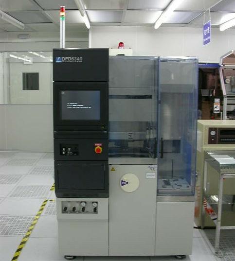
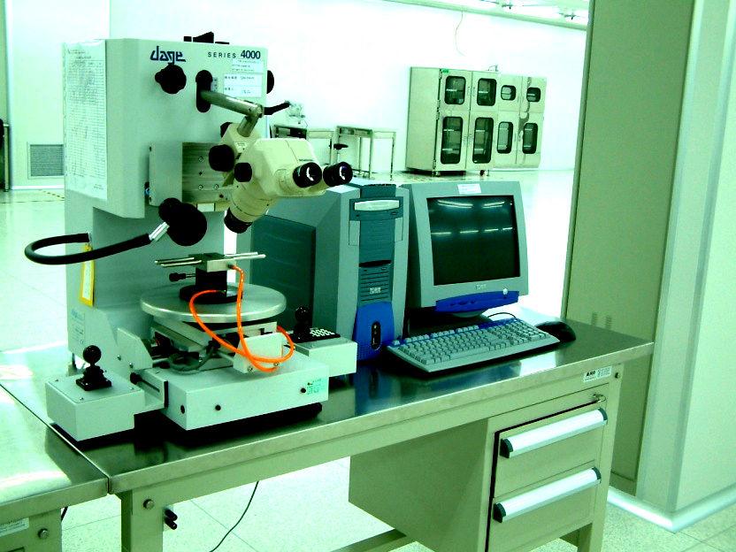
16 Grinding Die Bonder Die Sawer 16 Wire Bonder


17 Mold System PMC Ovens SMT Line Singulation Saw 17
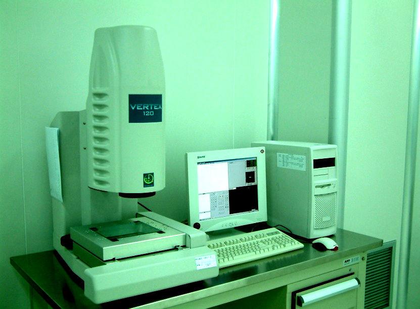
18 Microscope 3D Optic System Die Shear System Wire Pull Tester 18
19 Assembly capability (bond wire size (Au/Cu), bonding capability for single row/ dual row and offset pads, grinding capability, and so on) 19
20 Process Capability Process Item Process Capability Wafer Size 6'' / 8'' Wafer Grinding Minimum final thickness 4mils Parallelism TTV < 5um Thickness Variation between wafers <=10μm Wafer Size 4~8 inch Cutting Method through Cut/ Step Cut Wafer Sawing Minimum chip size cutting 0.2mm square DI water Resistivity >=10MΩ Chipping width <=10μ m Cutting street >50μ m Wafer Size 4 ~ 8'' Acceptable die size >0.2mm square Pick Type wafer mapping/ Ink Dot Die Bonding Bonding Type Epoxy type Epoxy Bleeding <10mils Epoxy thickness 5~40um Epoxy Voids within 5% in die area Die Placement Accuracy Theta :±0.5º ;X/Y:± 2 mils 20
21 Process Capability Process Item Process Capability Wire Bonding (Au wire) Wire Bonding (Cu wire) Fine Pitch Capability wire size Loop height control Bonding Frequency Bond placement repeatability Bond pad pitch (single/ dual row) Bond pad openning Staggered bond Wire Span Fine Pitch Capability wire size Loop height control Bonding Frequency Bond placement repeatability Bond pad pitch (single/ dual row) Bond pad openning Staggered bond Wire Span 45um 0.7 ~2.0 mils ±25um 138K HZ 3um 45um 40um 30um ~8mm 60um 0.9~1.2 mils ±25um 138K HZ 3um 60um 50um 40um ~10mm 21
22 Process Capability Process Item Process Capability Die Coating Viscosity 500 ~ cps Sealing Accuracy 4mils Molding thickness 0.55/0.75/0.90mm Lead frame handling thickness 0.15mm Molding Wire sweep <5% Body offset/ off center <1 mil Marking Symbol Laser/ Ink Plating Plating composition Pb/Sn(85/15%) (Apply to lead frmae type) Lead free capability Pure Tin (100%), Sn/Bi(98/2%), Sn/Cu(99/1%) Trim \ Forming Coplanarity <4mils Solder Thickness 0.12 ± 0.06 mm SMT Component size Min Mount for SMD ± 2.0 mils 22
23 Low Cost Solution Material evaluation ex. To study low cost materials with high quality Au wire Cu wire To co-work with customer to reduce the gold wire dimension Package design ex. Smaller package design to increase product value QFP QFN SOT TSOT To integrate more chips and components in one package (SIP design) 23
24 Rapid Product Design/Phase-in in 1. Capability: Stack die SIP design MEMS product design/production Product design 2. Sample making timeline: Available package: 1 week for sample making. New type lead frame/substrate: 4~6 weeks for prototype. New package/product: around 3 months (based on product requirement) 24
MICROELECTRONICS ASSSEMBLY TECHNOLOGIES. The QFN Platform as a Chip Packaging Foundation
 West Coast Luncheon January 15, 2014. PROMEX PROMEX INDUSTRIES INC. MICROELECTRONICS ASSSEMBLY TECHNOLOGIES The QFN Platform as a Chip Packaging Foundation 3075 Oakmead Village Drive Santa Clara CA Ɩ 95051
HANA Semiconductor (Ayutthaya) Co. Ltd. Die Design Rule For Assembly Of Plastic Devices
 Co. Ltd. Die Design Rule For Assembly Of Plastic Devices") HANA Semiconductor (Ayutthaya) Co. Ltd. Die Design Rule For Assembly Of Plastic Devices 1.0 PURPOSE : 1.1 To define the rules to be observed to facilitate review of process ability of devices prior to
HANA Semiconductor (Ayutthaya) Co. Ltd. Die Design Rule For Assembly Of Plastic Devices 1.0 PURPOSE : 1.1 To define the rules to be observed to facilitate review of process ability of devices prior to
SiP packaging technology of intelligent sensor module. Tony li
 SiP packaging technology of intelligent sensor module Tony li 2016.9 Contents What we can do with sensors Sensor market trend Challenges of sensor packaging SiP technology to overcome challenges Overview
Data Sheet _ R&D. Rev Date: 8/17
 Data Sheet _ R&D Rev Date: 8/17 Micro Bump In coming years the interconnect density for several applications such as micro display, imaging devices will approach the pitch 10um and below. Many research
Chapter 11 Testing, Assembly, and Packaging
 Chapter 11 Testing, Assembly, and Packaging Professor Paul K. Chu Testing The finished wafer is put on a holder and aligned for testing under a microscope Each chip on the wafer is inspected by a multiple-point
Compression Molding. Solutions for 3D TSV and other advanced packages as well as cost savings for standard package applications
 Compression Molding Solutions for 3D TSV and other advanced packages as well as cost savings for standard package applications 1. Company Introduction 2. Package Development Trend 3. Compression FFT Molding
Two major features of this text
 Two major features of this text Since explanatory materials are systematically made based on subject examination questions, preparation
TN008. PCB Design Guidelines for 2x2 LGA Sensors. Introduction. 2x2 LGA Package Marking
 PCB Design Guidelines for 2x2 LGA Sensors Introduction This technical note is intended to provide information about Kionix s 2 x 2 mm LGA packages and guidelines for developing PCB land pattern layouts.
Interconnection Challenge in Wire Bonding Ag alloy wire. Jensen Tsai / 蔡瀛洲, SPIL, Taiwan
 1 Interconnection Challenge in Wire Bonding Ag alloy wire Jensen Tsai / 蔡瀛洲, SPIL, Taiwan 2 Content Ag Alloy Wire Type Market Ag Alloy Wire Benefits Workability and Reliability Performance IMC behavior
CHAPTER 11: Testing, Assembly, and Packaging
 Chapter 11 1 CHAPTER 11: Testing, Assembly, and Packaging The previous chapters focus on the fabrication of devices in silicon or the frontend technology. Hundreds of chips can be built on a single wafer,
B. Flip-Chip Technology
 B. Flip-Chip Technology B1. Level 1. Introduction to Flip-Chip techniques B1.1 Why flip-chip? In the development of packaging of electronics the aim is to lower cost, increase the packaging density, improve
Stack Die CSP Interconnect Challenges Flynn Carson, Glenn Narvaez, HC Choi, and DW Son ChipPAC, Inc.
 Stack Die CSP Interconnect Challenges Flynn Carson, Glenn Narvaez, HC Choi, and DW Son ChipPAC, Inc. IEEE/CPMT Seminar Overview 4 Stacked die Chip Scale Packages (CSPs) enable more device functionality
Processes for Flexible Electronic Systems
 Processes for Flexible Electronic Systems Michael Feil Fraunhofer Institut feil@izm-m.fraunhofer.de Outline Introduction Single sheet versus reel-to-reel (R2R) Substrate materials R2R printing processes
Laminate Based Fan-Out Embedded Die Technologies: The Other Option
 Laminate Based Fan-Out Embedded Die Technologies: The Other Option Theodore (Ted) G. Tessier, Tanja Karila*, Tuomas Waris*, Mark Dhaenens and David Clark FlipChip International, LLC 3701 E University Drive
Application Bulletin 240
 Application Bulletin 240 Design Consideration CUSTOM CAPABILITIES Standard PC board fabrication flexibility allows for various component orientations, mounting features, and interconnect schemes. The starting
Specifications subject to change Packaging
 VCSEL Standard Product Packaging Options All standard products are represented in the table below. The Part Number for a standard product is determined by replacing the x in the column Generic Part Number
Trends in Advanced Packaging Technologies An IMAPS UK view
 Trends in Advanced Packaging Technologies An IMAPS UK view Andy Longford Chair IMAPS UK 2007 9 PandA Europe IMAPS UK IeMRC Interconnection event December 2008 1 International Microelectronics And Packaging
Assembly/Packagng RF-PCB. Thick Film. Thin Film. Screening/Test. Design Manual
 Thick Film Thin Film RF-PCB Assembly/Packagng Screening/Test Design Manual RHe Design Manual The following rules are effective for the draft of circuit boards and hybrid assemblies. The instructions are
General Rules for Bonding and Packaging
 General Rules for Bonding and Packaging at the Else Kooi Laboratory 3 CONTENT Rules for assembly at EKL 4 Introduction to assembly 5 Rules for Saw Lane 7 Rules for Chip Size 8 Rules for Bondpads 9 Rules
APPLICATION NOTE 6381 ORGANIC LAND GRID ARRAY (OLGA) AND ITS APPLICATIONS
 AND ITS APPLICATIONS") Keywords: OLGA, SMT, PCB design APPLICATION NOTE 6381 ORGANIC LAND GRID ARRAY (OLGA) AND ITS APPLICATIONS Abstract: This application note discusses Maxim Integrated s OLGA and provides the PCB design and
Keywords: OLGA, SMT, PCB design APPLICATION NOTE 6381 ORGANIC LAND GRID ARRAY (OLGA) AND ITS APPLICATIONS Abstract: This application note discusses Maxim Integrated s OLGA and provides the PCB design and
!"#$"%&' ()#*+,-+.&/0(
#*+,-+.&/0(") !"#$"%&' ()#*+,-+.&/0( Multi Chip Modules (MCM) or Multi chip packaging Industry s first MCM from IBM. Generally MCMs are horizontal or two-dimensional modules. Defined as a single unit containing two
!"#$"%&' ()#*+,-+.&/0( Multi Chip Modules (MCM) or Multi chip packaging Industry s first MCM from IBM. Generally MCMs are horizontal or two-dimensional modules. Defined as a single unit containing two
TAIPRO Engineering. Speaker: M. Saint-Mard Managing director. TAIlored microsystem improving your PROduct
 TAIPRO Engineering MEMS packaging is crucial for system performance and reliability Speaker: M. Saint-Mard Managing director TAIPRO ENGINEERING SA Michel Saint-Mard Administrateur délégué m.saintmard@taipro.be
The Future of Packaging and Cu Wire Bonding Advances. Ivy Qin
 The Future of Packaging and Cu Wire Bonding Advances Ivy Qin Introduction Semiconductors have been around for over 70 years Packaging is playing a more and more important role, providing low cost high
450mm and Moore s Law Advanced Packaging Challenges and the Impact of 3D
 450mm and Moore s Law Advanced Packaging Challenges and the Impact of 3D Doug Anberg VP, Technical Marketing Ultratech SOKUDO Lithography Breakfast Forum July 10, 2013 Agenda Next Generation Technology
EFFECTS OF USG CURRENT AND BONDING LOAD ON BONDING FORMATION IN QFN STACKED DIE PACKAGE. A. Jalar, S.A. Radzi and M.A.A. Hamid
 Solid State Science and Technology, Vol. 16, No 2 (2008) 65-71 EFFECTS OF USG CURRENT AND BONDING LOAD ON BONDING FORMATION IN QFN STACKED DIE PACKAGE A. Jalar, S.A. Radzi and M.A.A. Hamid School of Applied
Benzocyclobutene Polymer dielectric from Dow Chemical used for wafer-level redistribution.
 Glossary of Advanced Packaging: ACA Bare Die BCB BGA BLT BT C4 CBGA CCC CCGA CDIP or CerDIP CLCC COB COF CPGA Anisotropic Conductive Adhesive Adhesive with conducting filler particles where the electrical
POSSUM TM Die Design as a Low Cost 3D Packaging Alternative
 POSSUM TM Die Design as a Low Cost 3D Packaging Alternative The trend toward 3D system integration in a small form factor has accelerated even more with the introduction of smartphones and tablets. Integration
Advances in stacked-die packaging
 pg.10-15-carson-art 16/6/03 4:12 pm Page 1 The stacking of die within IC packages, primarily Chip Scale Packages (CSP) Ball Grid Arrays (BGAs) has evolved rapidly over the last few years. The now standard
SMT Assembly Considerations for LGA Package
 SMT Assembly Considerations for LGA Package 1 Solder paste The screen printing quantity of solder paste is an key factor in producing high yield assemblies. Solder Paste Alloys: 63Sn/37Pb or 62Sn/36Pb/2Ag
FEATURES DESCRIPTION ABSOLUTE MAXIMUM RATINGS. T AMB = +25 C ( Unless otherwise specified )
") Monolithic PIN SP5T Diode Switch FEATURES Ultra Broad Bandwidth: 50MHz to 26GHz 1.0 db Insertion Loss 30 db Isolation at 20GHz Reliable. Fully Monolithic Glass Encapsulated Construction DESCRIPTION The
Monolithic PIN SP5T Diode Switch FEATURES Ultra Broad Bandwidth: 50MHz to 26GHz 1.0 db Insertion Loss 30 db Isolation at 20GHz Reliable. Fully Monolithic Glass Encapsulated Construction DESCRIPTION The
SOLDER BUMP FLIP CHIP BONDING FOR PIXEL DETECTOR HYBRIDIZATION
 SOLDER BUMP FLIP CHIP BONDING FOR PIXEL DETECTOR HYBRIDIZATION Jorma Salmi and Jaakko Salonen VTT Information Technology Microelectronics P.O. Box 1208 FIN-02044 VTT, Finland (visiting: Micronova, Tietotie
سمینار درس تئوری و تکنولوژی ساخت
 نام خدا به 1 سمینار درس تئوری و تکنولوژی ساخت Wire Bonding استاد : جناب آقای محمدنژاد دکتر اردیبهشت 93 2 3 Content IC interconnection technologies Whats wirebonding Wire Bonding Processes Thermosonic Wirebond
High Frequency (up to 40 GHz) Resistor, Thin Film Surface Mount Chip
 Resistor, Thin Film Surface Mount Chip") FC High Frequency (up to 40 GHz) Resistor, Thin Film Surface Mount Chip FC series chip resistors are designed with low internal reactance. They function as almost pure resistors on a very high range of
FC High Frequency (up to 40 GHz) Resistor, Thin Film Surface Mount Chip FC series chip resistors are designed with low internal reactance. They function as almost pure resistors on a very high range of
Min Tao, Ph. D, Ashok Prabhu, Akash Agrawal, Ilyas Mohammed, Ph. D, Bel Haba, Ph. D Oct , IWLPC
 PACKAGE-ON-PACKAGE INTERCONNECT FOR FAN-OUT WAFER LEVEL PACKAGES Min Tao, Ph. D, Ashok Prabhu, Akash Agrawal, Ilyas Mohammed, Ph. D, Bel Haba, Ph. D Oct 18-20 2016, IWLPC 1 Outline Laminate to Fan-Out
Innovations Push Package-on-Package Into New Markets. Flynn Carson. STATS ChipPAC Inc Kato Rd Fremont, CA 94538
 Innovations Push Package-on-Package Into New Markets by Flynn Carson STATS ChipPAC Inc. 47400 Kato Rd Fremont, CA 94538 Copyright 2010. Reprinted from Semiconductor International, April 2010. By choosing
Custom MMIC Packaging Solutions for High Frequency Thermally Efficient Surface Mount Applications.
 Custom MMIC Packaging Solutions for High Frequency Thermally Efficient Surface Mount Applications. Steve Melvin Principal Engineer Teledyne-Labtech 8 Vincent Avenue, Crownhill, Milton Keynes, MK8 AB Tel
Assembly Instructions for SCC1XX0 series
 Technical Note 82 Assembly Instructions for SCC1XX0 series TABLE OF CONTENTS Table of Contents...1 1 Objective...2 2 VTI's 32-lead Dual In-line Package (DIL-32)...2 3 DIL-32 Package Outline and Dimensions...2
The Future of Packaging ~ Advanced System Integration
 The Future of Packaging ~ Advanced System Integration Enabling a Microelectronic World R. Huemoeller SVP, Adv. Product / Platform Develop June 2013 Product Segments End Market % Share Summary 2 New Product
Fraunhofer IZM - ASSID
 FRAUNHOFER-INSTITUT FÜR Zuverlässigkeit und Mikrointegration IZM Fraunhofer IZM - ASSID All Silicon System Integration Dresden Heterogeneous 3D Wafer Level System Integration 3D system integration is one
Assembly Instructions for SCA6x0 and SCA10x0 series
 Technical Note 71 Assembly Instructions for SCA6x0 and SCA10x0 series TABLE OF CONTENTS Table of Contents...1 1 Objective...2 2 VTI'S DIL-8 and DIL-12 packages...2 3 Package Outline and Dimensions...2
High Efficient Heat Dissipation on Printed Circuit Boards. Markus Wille, R&D Manager, Schoeller Electronics Systems GmbH
 High Efficient Heat Dissipation on Printed Circuit Boards Markus Wille, R&D Manager, Schoeller Electronics Systems GmbH m.wille@se-pcb.de Introduction 2 Heat Flux: Q x y Q z The substrate (insulation)
FLIP CHIP LED SOLDER ASSEMBLY
 As originally published in the SMTA Proceedings FLIP CHIP LED SOLDER ASSEMBLY Gyan Dutt, Srinath Himanshu, Nicholas Herrick, Amit Patel and Ranjit Pandher, Ph.D. Alpha Assembly Solutions South Plainfield,
Electroless Bumping for 300mm Wafers
 Electroless Bumping for 300mm Wafers T. Oppert Internepcon 2006 Tokyo Big Sight, Japan Outline Short Company Profile Electroless Ni/Au Under Bump Metallization UBM for Copper Devices Solder Bumping: Stencil
Image Sensor Advanced Package Solution. Prepared by : JL Huang & KingPak RD division
 Image Sensor Advanced Package Solution Prepared by : JL Huang & KingPak RD division Contents CMOS image sensor marketing overview Comparison between different type of CMOS image sensor package Overview
UMS User guide for bare dies GaAs MMIC. storage, pick & place, die attach and wire bonding
 UMS User guide for bare dies GaAs MMIC storage, pick & place, die attach and wire bonding Ref. : AN00014097-07 Apr 14 1/10 Specifications subject to change without notice United Monolithic Semiconductors
Green. Pin Diagram. Part Number Compliance Case Packaging HDS20M-13 Commercial HDS 5,000/Tape & Reel
 Green 2A SURFACE MOUNT GLASS PASSIVATED BRIDGE RECTIFIER Product Summary (@T A = +25 C) V RRM (V) I O (A) V F (V) I R (μa) 1000 2 0.95 5 Features and Benefits Glass Passivated Die Construction Miniature
IMAPS NE 45 A HETEROGENEOUS SIP SOLUTION FOR RF APPLICATIONS
 IMAPS NE 45 A HETEROGENEOUS SIP SOLUTION FOR RF APPLICATIONS May 1st 2018 Justin C. Borski i3 Microsystems Inc. justin.borski@i3microsystems.com A HETEROGENEOUS SIP SOLUTION FOR RF APPLICATIONS Presentation
INDEX BY DEVICE TYPE OF REGISTERED MICROELECTRONIC OUTLINES (MO) REGISTRATION NO.
 REGISTRATION NO.") AXIAL QUAD 1.56 mm (.065") Pitch MO-010 Pins: 12 2.54 mm (.100") Pitch MO-017 Pins: 52, 64 BALL GRID ARRAY (BGA) Tape BGA 1, 1.27. 1.5 mm Pitch Pins: 100 thru 2401 Plastic BGA 1, 1.27, 1.5mm Pitch Pins:
AXIAL QUAD 1.56 mm (.065") Pitch MO-010 Pins: 12 2.54 mm (.100") Pitch MO-017 Pins: 52, 64 BALL GRID ARRAY (BGA) Tape BGA 1, 1.27. 1.5 mm Pitch Pins: 100 thru 2401 Plastic BGA 1, 1.27, 1.5mm Pitch Pins:
BOARD DESIGN, SURFACE MOUNT ASSEMBLY AND BOARD LEVEL RELIABILITY ASPECTS OF FUSIONQUAD TM PACKAGES
 BOARD DESIGN, SURFACE MOUNT ASSEMBLY AND BOARD LEVEL RELIABILITY ASPECTS OF FUSIONQUAD TM PACKAGES Ahmer Syed 1, Sundar Sethuraman 2, WonJoon Kang 1, Gary Hamming 1, YeonHo Choi 1 1 Amkor Technology, Inc.
Introduction to Wire-Bonding
 Introduction to Wire-Bonding Wire bonding is a kind of friction welding Material are connected via friction welding Advantage: Different materials can be connected to each other widely used, e.g. in automobile
Electronic materials and components-semiconductor packages
 Electronic materials and components-semiconductor packages Semiconductor back-end processes We will learn much more about semiconductor back end processes in subsequent modules, but you need to understand
50 Ω nominal input / conjugate match balun to nrf51422-qfaa, nrf24le1, nrf51822-qfaa/ab, with integrated harmonic filter
 50 Ω nominal input / conjugate match balun to nrf51422-qfaa, nrf24le1, nrf51822-qfaa/ab, with integrated harmonic filter Datasheet - production data Features 50 Ω nominal input / conjugate match to Nordic
Chapter 2. Literature Review
 Chapter 2 Literature Review 2.1 Development of Electronic Packaging Electronic Packaging is to assemble an integrated circuit device with specific function and to connect with other electronic devices.
Tape Automated Bonding
 Tape Automated Bonding Introduction TAB evolved from the minimod project begun at General Electric in 1965, and the term Tape Automated Bonding was coined by Gerard Dehaine of Honeywell Bull in 1971. The
An Introduction to Electronics Systems Packaging. Prof. G. V. Mahesh. Department of Electronic Systems Engineering
 An Introduction to Electronics Systems Packaging Prof. G. V. Mahesh Department of Electronic Systems Engineering India Institute of Science, Bangalore Module No. # 02 Lecture No. # 08 Wafer Packaging Packaging
Laser Solder Attach for Optoelectronics Packages
 1 Laser Solder Attach for Optoelectronics Packages Elke Zakel, Lars Titerle, Thomas Oppert, Ronald G. Blankenhorn* Pac Tech Packaging Technologies GmbH Am Schlangenhorst 15-17, Germany Phone:+ 49 (0) 33
SWTW 2000, June Assessing Pad Damage and Bond Integrity for Fine Pitch Probing
 SWTW 2000, June 11-14 Assessing Pad Damage and Bond Integrity for Fine Pitch Probing Dean Gahagan, Pyramid Probe Division, Cascade Microtech & Lee Levine, Kulicke & Soffa Industries Challenges of die shrinks
Fan-Out Solutions: Today, Tomorrow the Future Ron Huemoeller
 Fan-Out Solutions: Today, Tomorrow the Future Ron Huemoeller Corporate Vice President, WW RnD & Technology Strategy 1 In the Beginning ewlb 2 Fan Out Packaging Emerges Introduction of Fan Out (ewlb) Marketed
Flip-Chip for MM-Wave and Broadband Packaging
 1 Flip-Chip for MM-Wave and Broadband Packaging Wolfgang Heinrich Ferdinand-Braun-Institut für Höchstfrequenztechnik (FBH) Berlin / Germany with contributions by F. J. Schmückle Motivation Growing markets
 Distributed by: www.jameco.com 1-8-831-4242 The content and copyrights of the attached material are the property of its owner. 35mW SURFACE MOUNT ENER DIODE Features Planar Die Construction 35mW Power
MASW P. SURMOUNT PIN Diode Switch Element with Thermal Terminal. Features. Description. Ordering Information 2.
 Features Specified Bandwidth: 45MHz 2.5GHz Useable 30MHz to 3.0GHz Low Loss 40dB High C.W. Incident Power, 50W at 500MHz High Input IP3, +66dBm @ 500MHz Unique Thermal Terminal for
First Demonstration of Panel Glass Fan-out (GFO) Packages for High I/O Density and High Frequency Multi-Chip Integration
 Packages for High I/O Density and High Frequency Multi-Chip Integration") First Demonstration of Panel Glass Fan-out (GFO) Packages for High I/O Density and High Frequency Multi-Chip Integration Tailong Shi, Chintan Buch,Vanessa Smet, Yoichiro Sato, Lutz Parthier, Frank Wei
First Demonstration of Panel Glass Fan-out (GFO) Packages for High I/O Density and High Frequency Multi-Chip Integration Tailong Shi, Chintan Buch,Vanessa Smet, Yoichiro Sato, Lutz Parthier, Frank Wei
True Three-Dimensional Interconnections
 True Three-Dimensional Interconnections Satoshi Yamamoto, 1 Hiroyuki Wakioka, 1 Osamu Nukaga, 1 Takanao Suzuki, 2 and Tatsuo Suemasu 1 As one of the next-generation through-hole interconnection (THI) technologies,
Market and technology trends in advanced packaging
 Close Market and technology trends in advanced packaging Executive OVERVIEW Recent advances in device miniaturization trends have placed stringent requirements for all aspects of product manufacturing.
Green. Part Number Compliance Case Packaging DBF Commercial DBF 3,000/Tape & Reel
 Green 3A SURFACE MOUNT GLASS PASSIVATED BRIDGE RECTIFIER Product Summary (@T A = +25 C) V RRM (V) I O (A) V F (V) I R (μa),000 3.0 5 Features and Benefits Glass Passivated Die Construction Miniature Package
Features. Preliminary. = +25 C, IF = 1 GHz, LO = +13 dbm*
 Typical Applications Features The is ideal for: Test Equipment & Sensors Point-to-Point Radios Point-to-Multi-Point Radios Military & Space Functional Diagram Wide IF Bandwidth: DC - 17 GHz Input IP3:
Packaging Roadmap: The impact of miniaturization. Bob Pfahl, inemi Celestica-iNEMI Technology Forum May 15, 2007
 Packaging Roadmap: The impact of miniaturization Bob Pfahl, inemi Celestica-iNEMI Technology Forum May 15, 2007 The Challenges for the Next Decade Addressing the consumer experience using the converged
Power Integration in Circuit Board
 Power Integration in Circuit Board APEC 2015 AT & S Austria Technologie & Systemtechnik Aktiengesellschaft Fabriksgasse13 A-8700 Leoben Tel +43 (0) 3842 200-0 E-Mail info@ats.net www.ats.net PICB APEC
Advanced Packaging Equipment Solder Jetting & Laser Bonding
 Advanced Packaging Equipment Solder Jetting & Laser Bonding www.pactech.comw.pactech.com PacTech Packaging Technologies Pioneering in laser solder jetting technologies since 1995 Our mission is to reshape
TDDB Time Depending Dielectric Breakdown. NBTI Negative Bias Temperature Instability. Human Body Model / Machine Model
 For integrated circuits or discrete semiconductors select Amkor-Kr to ASECL Assembly Transfer with Cu wire bonds ID Type of change No Yes AC TC SD Headings ANY A2 A3 A4 A5 A6 B1 B2 B3 C1 C2 C3 C4 C5 C6
CHV3241-QDG RoHS COMPLIANT
 RoHS COMPLIANT Description Fully Integrated HBT GaAs Monolithic Microwave IC In QFN package The is a monolithic multifunction circuit suitable for frequency generation. It integrates an X-band push-push
HOW DOES PRINTED SOLDER PASTE VOLUME AFFECT SOLDER JOINT RELIABILITY?
 HOW DOES PRINTED SOLDER PASTE VOLUME AFFECT SOLDER JOINT RELIABILITY? ABSTRACT Printing of solder paste and stencil technology has been well studied and many papers have been presented on the topic. Very
Hermetic Packaging Solutions using Borosilicate Glass Thin Films. Lithoglas Hermetic Packaging Solutions using Borosilicate Glass Thin Films
 Hermetic Packaging Solutions using Borosilicate Glass Thin Films 1 Company Profile Company founded in 2006 ISO 9001:2008 qualified since 2011 Headquarters and Production in Dresden, Germany Production
WLP User's Guide. CMOS IC Application Note. Rev.1.0_03. ABLIC Inc., 2014
 CMOS IC Application Note WLP User's Guide ABLIC Inc., 2014 This document is a reference manual that describes the handling of the mounting of super-small WLP (Wafer Level Package) for users in the semiconductor
Bob Willis Process Guides
 What is a Printed Circuit Board Pad? What is a printed circuit board pad, it may sound like a dumb question but do you stop to think what it really does and how its size is defined and why? A printed circuit
User s Guide to. Centre for Materials for Electronics Technology Panchawati, Off Pashan Road, Pune September Version 2.
 User s Guide to Centre for Materials for Electronics Technology Panchawati, Off Pashan Road, Pune 411008 September 2013 Version 2.1 Contents 1 Designing of LTCC Structures and Design Rules... 01 1.1 Guidelines
The Smallest Form Factor GPS for Mobile Devices
 2017 IEEE 67th Electronic Components and Technology Conference The Smallest Form Factor GPS for Mobile Devices Eb Andideh 1, Chuck Carpenter 2, Jason Steighner 2, Mike Yore 2, James Tung 1, Lynda Koerber
Flip Chip Bonding Using Sony Anisotropic Conductive Film (ACF) FP1526Y
 FP1526Y") Flip Chip Bonding Using Sony Anisotropic Conductive Film (ACF) FP1526Y Purpose: Author: Rekha S. Pai (07/29/03) To use ACF as an interconnection method for attaching dice to substrates. Direct electrical
Flip Chip Bonding Using Sony Anisotropic Conductive Film (ACF) FP1526Y Purpose: Author: Rekha S. Pai (07/29/03) To use ACF as an interconnection method for attaching dice to substrates. Direct electrical
SHELLCASE-TYPE WAFER-LEVEL PACKAGING SOLUTIONS: RF CHARACTERIZATION AND MODELING
 SHELLCASE-TYPE WAFER-LEVEL PACKAGING SOLUTIONS: RF CHARACTERIZATION AND MODELING M Bartek 1, S M Sinaga 1, G Zilber 2, D Teomin 2, A Polyakov 1, J N Burghartz 1 1 Delft University of Technology, Lab of
New Wave SiP solution for Power
 New Wave SiP solution for Power Vincent Lin Corporate R&D ASE Group APEC March 7 th, 2018 in San Antonio, Texas. 0 Outline Challenges Facing Human Society Energy, Environment and Traffic Autonomous Driving
PAGE 1/6 ISSUE Jul SERIES Micro-SPDT PART NUMBER R516 XXX 10X R 516 _ 1 0 _
 PAGE 1/6 ISSUE Jul-24-2017 SERIES Micro-SPDT PART NUMBER R516 XXX 10X R516 series: the RAMSES concept merges with the SLIM LINE technology, breaking up the frequency limits of SMT switches : - FULL SMT
Design and Development of True-CSP
 Design and Development of True-CSP *Kolan Ravi Kanth, Francis K.S. Poh, B.K. Lim, Desmond Y.R. Chong, Anthony Sun, H.B. Tan United Test & Assembly Center Ltd (UTAC) 5 Serangoon North Ave 5, Singapore 554916
Molded, 25 mil Pitch, Dual-In-Line Thin Film Resistor, Surface Mount Network
 OSOP Molded, 25 mil Pitch, Dual-In-Line Thin Film Resistor, Surface Mount Network OSOP Series resistor networks feature a space saving 25 mil lead pitch versus the current 50 mil pitch standard. This allows
Application Note AN-1011
 AN-1011 Board Mounting Application Note for 0.800mm Pitch Devices For part numbers IRF6100, IRF6100PBF, IR130CSP, IR130CSPPBF, IR140CSP, IR140CSPPBF, IR1H40CSP, IR1H40CSPPBF By Hazel Schofield and Philip
LeBen Semiconductor Inc. PRODUCTS. 216, Doha-ri Munbaek-myeon, Jincheon-gun, Chungcheongbuk-do, , KOREA http ://
 LeBen Semiconductor Inc. PRODUCTS 216, Doha-ri Munbaek-myeon, Jincheon-gun, Chungcheongbuk-do, 365-861, KOREA http :// www.lebensemi.com Company Intoduction Company name : LeBen Semiconductor Inc. President
ARCHIVE Brandon Prior Senior Consultant Prismark Partners ABSTRACT
 ARCHIVE 2010 LOW COST, SMALL FORM FACTOR PACKAGING by Brandon Prior Senior Consultant Prismark Partners W ABSTRACT hile size reduction and performance improvement are often the drivers of new package and
Thinning of IC chips
 1 Thinning of IC chips Annette Teng CORWIL TECHNOLOGY CORP. 1635 McCarthy Blvd. Milpitas, CA 95135 2 CONTENT Industry Demand for thinness Method to achieve ultrathin dies Mechanical testing of ultrathin
Yole Developpement. Developpement-v2585/ Publisher Sample
 Yole Developpement http://www.marketresearch.com/yole- Developpement-v2585/ Publisher Sample Phone: 800.298.5699 (US) or +1.240.747.3093 or +1.240.747.3093 (Int'l) Hours: Monday - Thursday: 5:30am - 6:30pm
C 2 B 1 E 1 E 2 B 2 C 1. Top View
 MMDT446 COMPLEMENTARY NPN / PNP SMALL SIGNAL SURFACE MOUNT TRANSISTOR Features Complementary Pair One 424-Type NPN One 426-Type PNP Epitaxial Planar Die Construction Ideal for Medium Power Amplification
Features. = +25 C, Vdd = 5V, Vgg1 = Vgg2 = Open
 v3.117 HMC441LM1 Typical Applications The HMC441LM1 is a medium PA for: Point-to-Point Radios Point-to-Multi-Point Radios VSAT LO Driver for HMC Mixers Military EW & ECM Functional Diagram Vgg1, Vgg2:
Chapter 7 Introduction to 3D Integration Technology using TSV
 Chapter 7 Introduction to 3D Integration Technology using TSV Jin-Fu Li Department of Electrical Engineering National Central University Jungli, Taiwan Outline Why 3D Integration An Exemplary TSV Process
PAGE 1/6 ISSUE SERIES Micro-SPDT PART NUMBER R516 XXX 10X. (All dimensions are in mm [inches]) R 516 _ 1 0 _
![PAGE 1/6 ISSUE SERIES Micro-SPDT PART NUMBER R516 XXX 10X. (All dimensions are in mm [inches]) R 516 _ 1 0 _](/thumbs/96/127769340.jpg "PAGE 1/6 ISSUE SERIES Micro-SPDT PART NUMBER R516 XXX 10X. (All dimensions are in mm [inches]) R 516 _ 1 0 _") PAGE 1/6 ISSUE 15-10-18 SERIES Micro-SPDT PART NUMBER R516 XXX 10X R516 series: the RAMSES concept merges with the SLIM LINE technology, breaking up the frequency limits of SMT switches : - FULL SMT TECHNOLOGY
PAGE 1/6 ISSUE 15-10-18 SERIES Micro-SPDT PART NUMBER R516 XXX 10X R516 series: the RAMSES concept merges with the SLIM LINE technology, breaking up the frequency limits of SMT switches : - FULL SMT TECHNOLOGY
TN016. PCB Design Guidelines for 5x5 DFN Sensors. Introduction. Package Marking
 PCB Design Guidelines for 5x5 DFN Sensors Introduction This technical note is intended to provide information about Kionix s 5 x 5 mm DFN (non wettable flank, i.e. standard) packages and guidelines for
sizes , 4 x 0402, 2 x 0603, 4 x 0603 RoHS compliant
 Product specification June 2, 2016 V.4 DATA SHEET ANTI-SULFURATED CHIP RESISTORS 122 (4Pin/2R) / 124 (Pin/4R) / 162 (4Pin/ 2R)/ 164 (Pin/ 4R) 5%, 1% sizes 2 0402, 4 x 0402, 2 x 0603, 4 x 0603 RoHS compliant
New Power MOSFET. 1. Introduction. 2. Application of Power MOSFETs. Naoto Fujisawa Toshihiro Arai Tadanori Yamada
 New Power MOSFET Naoto Fujisawa Toshihiro Arai Tadanori Yamada 1. Introduction Due to the finer patterns and higher integration of LSIs, functions that were used a few years ago in minicomputers have now
Green. Pin Diagram. Part Number Compliance Case Packaging MB10S-13 Commercial MBS 3,000/Tape & Reel
 Green 0.8A SURFACE MOUNT GLASS PASSIVATED BRIDGE RECTIFIER Product Summary (@T A = +25 C) V RRM (V) I O (A) V F (V) I R (μa) 000 0.8. 5 Description and Applications Features and Benefits Glass Passivated
50 ohm nominal input / conjugate match balun to nrf CEAA/CDAB/CFAC and nrf51422-ceaa/cdab/cfac. Description
 50 ohm nominal input / conjugate match balun to nrf51822- /CDAB/CFAC and nrf51422-/cdab/cfac Datasheet - production data Features Flip-Chip (5 bumps) package 50 Ω nominal input / conjugate match to Nordic
SESUB - Its Leadership In Embedded Die Packaging Technology
 SESUB - Its Leadership In Embedded Die Packaging Technology Sip Conference China 2018 TDK Corporation ECBC, PAF, SESUB BU Kofu, Japan October 17, 2018 Contents SESUB Introduction SESUB Process SESUB Quality
QUALITY SEMICONDUCTOR, INC.
 Q QUALITY SEMICONDUCTOR, INC. AN-20 Board Assembly Techniques for 0.4mm Pin Pitch Surface Mount Packages Application Note AN-20 The need for higher performance systems continues to push both silicon and
Technology & Manufacturing
 Technology & Manufacturing Jean-Marc Chery Chief Operating Officer Front-End Manufacturing Unique capability 2 Technology portfolio aligned with application focus areas Flexible IDM model with foundry