MID Manufacturing Process.
|
|
|
- Eleanor Hampton
- 5 years ago
- Views:
Transcription
1 3D Aerosol Jet Printing An Emerging MID Manufacturing Process. Dr. Martin Hedges Neotech Services MTP, Nuremberg, Germany
2 Aerosol Jet Printing Aerosol Jet Process Overview Current Application Examples 3D Printing Summary


3 Aerosol Jet Process Overview Aerosol Jet is CAD driven printing technique. Developed by Optomec Inc, Albuquerque, USA. >$12m in Aerosol Jet Technology & Product Development. 13 patents issued, 43+ pending Targeting $bn markets in Electronics, Energy, Life Science - Active Opportunities in Packaging, Display, Flex, Fuel Cell, Drug Discovery... Aerosol Jet 300CE


4 How the Process Works Functional ink is placed in the atomiser, gas flow creates an aerosol 2. Aerosol droplets ca.1-5μm, larger droplets return to ink (gravity effect) 3. The aerosol is carried to the deposition head, excess gas removed 4. The aerosol is focussed inside the nozzle by a secondary gas flow (sheath gas)

5 Aerosol Jet Characteristics 150μm Focussed Aerosol Beam No contact to nozzle Natural stand-off from substrate
6 Aerosol Jet Characteristics Too close - line spreads Ideal- line width constant with height 50 Too far away - turbulent mixing, line widens dth (micr rons) Line Wi Focal Length Height of Nozzle above Substrate (mm)


7 Conformal Deposition 60μm lines into 500μm trench Nozzle standoff distance of ca. 5mm and long focal length allows conformal deposition with no change in Z-height.

.")

8 Scalability Line Width Trials underway to reduce minimum line width to 5µm and below. Wide area nozzle development to print line widths 3mm+ (single pass). Current Line width scalability through 3 orders of magnitude. Ultra fine lines µm Ag Grid on Glass


9 Wide Area Nozzles New contract signed with US Airforce for Wide Area Nozzles. Next step is 5cm wide swaths - ie: 50mm line width. Fallback is to develop a multi-nozzle/head approach for area coating. Wide Area Nozzle 3mm Ag on Si Wafer CAD Model Wide Area Nozzle
10 Examples of Materials Used
11 Application Areas Packaging and Assembly High Density Interconnects* Flip-Chip / Direct Die Attach Embedded / Integrated Passives Flex Circuits Meso-Dispensing Electronic Components Resistors, Capacitors and Inductors Micro-Antennae Micro-Batteries Electronic Devices Solar Cells* Displays* Fuel Cells Sensors & MEMS Hybrid Manufacture 3D Smart Structures Life Science Bio-Sensors* Micro-Arrays *Production Applications 2010
 Interconnects: 25micron line width")

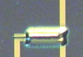
12 Connecting Stacked Dies (Replace Wire Bond or TSV) Interconnects: 25micron line width 10 microns thick Cross section for die interconnects. Insert shows close up of contact area.
13 Printed Interconnect Advantages Features Interconnects as small as 10μm at <30μm Pitch. Full Range of High Conductivity Materials. High Aspect Ratio for Low Resistivity. Supports Non-Planar and 3D Surfaces. Cost & Functional Advantages. Higher Frequencies* with Better Reliability than WireBond. Much Better Time-to-Market and Cost Structure vs. TSV. Reduced Form Factors vs. Package on Package. 3D Stacked Die Working with Leading Smart Phone Players for Multi-Chip Packages (Processor/Memory Chip Sets) *Supports HF without antenna effect. Enables Multi-Chip Packages that combine Processor with Memory, etc.
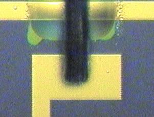
14 Touch Screen-Bridge/Jumper Circuit Pre-Patterned ITO 5mm Step 1: Print Insulator 30 microns wide Step 2: Print Nano-Silver 10 microns wide


15 Bridge Jumper on ITO REFLECTION Insulator Ag TRANSMISSION Step 1: Print Insulator 30 microns wide


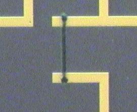
16 All-Printed OE Circuit 8 NAND Gates, 3 Inverters 2m m NAND Gate Inverter Crossover *Optomec Inc. collaboration with Dan Frisbie Group UMN


17 Printed Sensor Networks for Structural t Health Monitoring i Ag Strain Gauge on Al CuNi Strain Gauge COURTESY: Ag Strain Gauge on CFC


18 Printed Sensor Networks Simulation of Sensor Networks for Structural Health Monitoring Pt Strain Gauge FEA Combination with 3D MID Substrates Smart systems.
19 Printed Temperature Sensor Ag and Ni sensor structure


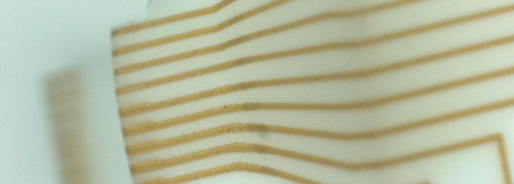


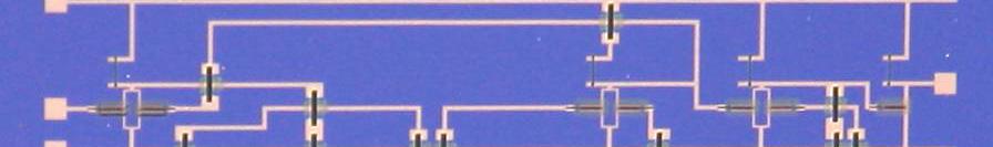
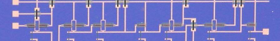
20 Example of Current 2 1/2D printing. Ceramic MID with Gold Ink ca 5mm ca. Interconnects ca. 100microns wide


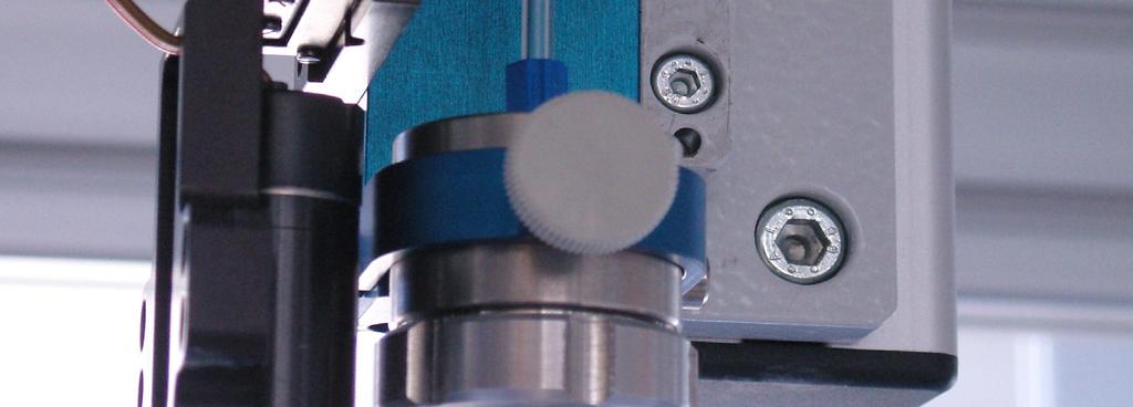
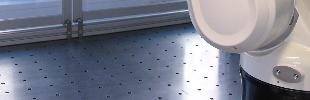

21 6-Axis 6 Axis Aerosol Jet Printer Test Part Part Gripper Nozzle Shutter Installed a 6-Axis Aerosol Jet printer which extends process capabilities to true, large area, 3D printing. Build volume: c. 850 x 1200 x 1000mm (x-y-z)


22 6-Axis Aerosol Jet Printer. AJ-6X System installed at the Electronics Lab of FAPS (Institute for Manufacturing Automation & Producton Systems), University Erlangen-Nuremberg. FAPS Lab has extensive expertise in electronic systems and MIDs. Aim for Synergistic Effect in 3D Electronics.
23 Summary Aerosol Jet Process Capability Non-contact, conformal deposition Scalability: Ultra fine printed fine features to wide area High Utility Wide range of materials compatibility Wide range of applications Scalability for volume manufacture New 6-Axis Printer opens the way for novel 3D Printed MIDs over large areas.
24 Thank You! Neotech Services MTP - Dr. Martin Hedges Tel: info@neotechservices.com
Fully Printed Conformal Antenna and Sensors on 3D Plastic, Ceramic, and Metallic Substrates. Mike O Reilly
 Fully Printed Conformal Antenna and Sensors on 3D Plastic, Ceramic, and Metallic Substrates Mike O Reilly imaps NE 2016 Antenna and sensor printing via Aerosol Jet Optomec has developed high volume 3D
Printed and Hybrid Integration
 Printed and Hybrid Integration Neil Chilton PhD Technical Director, Printed Electronics Limited, UK Neil.Chilton@PrintedElectronics.com Printed Electronics Limited (PEL) General Overview PEL was founded
Aerosol Jet technology opportunities
 Aerosol Jet technology opportunities Jiří Navrátil 1. Introduction history and formation 2. Aerosol Jet system 2.1 System components 2.2 Inks and substrates 3. Application of Aerosol Jet technology 4.
Printed Electronics. Applications
 Printed Electronics Research Through University-Industry Partnerships Outline Background on Printed Electronics (PE) Corporate Partnerships Raytheon UMass Lowell Research Institute (RURI) Printed Electronics
Flexible Hybrid Electronics Fabricated with High-Performance COTS ICs using RTI CircuitFilm TM Technology
 Flexible Hybrid Electronics Fabricated with High-Performance COTS ICs using RTI CircuitFilm TM Technology Scott Goodwin 1, Erik Vick 2 and Dorota Temple 2 1 Micross Advanced Interconnect Technology Micross
SiP packaging technology of intelligent sensor module. Tony li
 SiP packaging technology of intelligent sensor module Tony li 2016.9 Contents What we can do with sensors Sensor market trend Challenges of sensor packaging SiP technology to overcome challenges Overview
AEROSOL JET PRINTING SYSTEM FOR HIGH SPEED, NON-CONTACT FRONT SIDE METALLIZATION OF SILICON SOLAR CELLS
 AEROSOL JET PRINTING SYSTEM FOR HIGH SPEED, NON-CONTACT FRONT SIDE METALLIZATION OF SILICON SOLAR CELLS Bruce H. King and Stephen M. Barnes Optomec, Inc. 3911 Singer NE, Albuquerque, NM 87109, US Phone
Passive Direct Print Sensors
 Passive Wireless Sensor Technology Workshop June 6-7, 2012 Hyatt Regency, La Jolla, CA Passive Direct Print Sensors Mike Newton mnewton@nscrypt.com nscrypt Inc. Orlando, Florida University of Texas at
EMERGING SUBSTRATE TECHNOLOGIES FOR PACKAGING
 EMERGING SUBSTRATE TECHNOLOGIES FOR PACKAGING Henry H. Utsunomiya Interconnection Technologies, Inc. Suwa City, Nagano Prefecture, Japan henryutsunomiya@mac.com ABSTRACT This presentation will outline
B. Flip-Chip Technology
 B. Flip-Chip Technology B1. Level 1. Introduction to Flip-Chip techniques B1.1 Why flip-chip? In the development of packaging of electronics the aim is to lower cost, increase the packaging density, improve
MEMS in ECE at CMU. Gary K. Fedder
 MEMS in ECE at CMU Gary K. Fedder Department of Electrical and Computer Engineering and The Robotics Institute Carnegie Mellon University Pittsburgh, PA 15213-3890 fedder@ece.cmu.edu http://www.ece.cmu.edu/~mems
New wafer level stacking technologies and their applications
 New wafer level stacking technologies and their applications WDoD a new 3D PLUS technology Timothee Dargnies 3D PLUS USA Santa Clara, CA 1 Table of Contents Review of existing wafer level assembly processes
Printing versus coating technology Which way Printed Electronics with solution coating will go?
 Printing versus coating technology Which way Printed Electronics with solution coating will go? Frank Schäfer, Andrea Glawe, Dr. Daniel Eggerath, KROENERT GmbH& Co KG, Schuetzenstrasse 105, 22761 Hamburg
ACTIVE IMPLANTS. Glass Encapsulation
 ACTIVE IMPLANTS Glass Encapsulation OUTLINE Smart Implants Overview Cylindrical Glass Encapsulation CGE Planar Glass Encapsulation PGE Platform for Innovative Implantable Devices 5/7/2013 Glass Encapsulation
Figure 7 Dynamic range expansion of Shack- Hartmann sensor using a spatial-light modulator
 Figure 4 Advantage of having smaller focal spot on CCD with super-fine pixels: Larger focal point compromises the sensitivity, spatial resolution, and accuracy. Figure 1 Typical microlens array for Shack-Hartmann
Inkjet Filling of TSVs with Silver Nanoparticle Ink. Behnam Khorramdel, Matti Mäntysalo Tampere University of Technology ESTC 2014 Finland, Helsinki
 Inkjet Filling of TSVs with Silver Nanoparticle Ink Behnam Khorramdel, Matti Mäntysalo Tampere University of Technology ESTC 2014 Finland, Helsinki Outline Motivation for this study Inkjet in MEMS fabrication
!"#$"%&' ()#*+,-+.&/0(
#*+,-+.&/0(") !"#$"%&' ()#*+,-+.&/0( Multi Chip Modules (MCM) or Multi chip packaging Industry s first MCM from IBM. Generally MCMs are horizontal or two-dimensional modules. Defined as a single unit containing two
!"#$"%&' ()#*+,-+.&/0( Multi Chip Modules (MCM) or Multi chip packaging Industry s first MCM from IBM. Generally MCMs are horizontal or two-dimensional modules. Defined as a single unit containing two
AEROSOL JET PRINTING OF CONDUCTIVE EPOXY FOR 3D PACKAGING
 AEROSOL JET PRINTING OF CONDUCTIVE EPOXY FOR 3D PACKAGING Michael J. Renn, Ph.D., and Kurt K. Christenson, Ph.D. Optomec, Inc. St. Paul, MN, USA mrenn@optomec.com and kchristenson@optomec.com Donald Giroux
Fraunhofer IZM - ASSID
 FRAUNHOFER-INSTITUT FÜR Zuverlässigkeit und Mikrointegration IZM Fraunhofer IZM - ASSID All Silicon System Integration Dresden Heterogeneous 3D Wafer Level System Integration 3D system integration is one
Signal Integrity Modeling and Measurement of TSV in 3D IC
 Signal Integrity Modeling and Measurement of TSV in 3D IC Joungho Kim KAIST joungho@ee.kaist.ac.kr 1 Contents 1) Introduction 2) 2.5D/3D Architectures with TSV and Interposer 3) Signal integrity, Channel
The Future of Packaging ~ Advanced System Integration
 The Future of Packaging ~ Advanced System Integration Enabling a Microelectronic World R. Huemoeller SVP, Adv. Product / Platform Develop June 2013 Product Segments End Market % Share Summary 2 New Product
Microfabrication technologies for highly-laminated thick metallic cores and 3-D integrated windings
 Microfabrication technologies for highly-laminated thick metallic cores and 3-D integrated windings Florian Herrault Georgia Institute of Technology Atlanta, GA florian@gatech.edu http://mems.gatech.edu/msma
450mm and Moore s Law Advanced Packaging Challenges and the Impact of 3D
 450mm and Moore s Law Advanced Packaging Challenges and the Impact of 3D Doug Anberg VP, Technical Marketing Ultratech SOKUDO Lithography Breakfast Forum July 10, 2013 Agenda Next Generation Technology
Lecture 0: Introduction
 Lecture 0: Introduction Introduction Integrated circuits: many transistors on one chip. Very Large Scale Integration (VLSI): bucketloads! Complementary Metal Oxide Semiconductor Fast, cheap, low power
3D and Aerosol Printed Conductor Dielectric Full- 3D RF Metamaterials
 3D and Aerosol Printed Conductor Dielectric Full- 3D RF Metamaterials June 22, 2017 Jimmy Hester, Evan Nguyen, Jesse Tice, and Vesna Radisic Approved for Public Release: NG17-1180, 6/2/17 Outline Introduction
National Centre for Flexible Electronics
 National Centre for Flexible Electronics Tripartite Partnership Government FlexE Centre - A platform for a meaningful interaction between industry and academia. An interdisciplinary team that advances
shaping global nanofuture ULTRA-PRECISE PRINTING OF NANOMATERIALS
 shaping global nanofuture ULTRA-PRECISE PRINTING OF NANOMATERIALS WHO ARE WE? XTPL S.A. is a company operating in the nanotechnology segment. The interdisciplinary team of XTPL develops on a global scale
Disruptive Developments for Advanced Die Attach to Tackle the Challenges of Heterogeneous Integration
 Disruptive Developments for Advanced Die Attach to Tackle the Challenges of Heterogeneous Integration Hugo Pristauz & Andreas Mayr, Besi Austria presented by: Stefan Behler, Besi Switzerland ECTC 2018
Innovations Push Package-on-Package Into New Markets. Flynn Carson. STATS ChipPAC Inc Kato Rd Fremont, CA 94538
 Innovations Push Package-on-Package Into New Markets by Flynn Carson STATS ChipPAC Inc. 47400 Kato Rd Fremont, CA 94538 Copyright 2010. Reprinted from Semiconductor International, April 2010. By choosing
Processes for Flexible Electronic Systems
 Processes for Flexible Electronic Systems Michael Feil Fraunhofer Institut feil@izm-m.fraunhofer.de Outline Introduction Single sheet versus reel-to-reel (R2R) Substrate materials R2R printing processes
CMP for More Than Moore
 2009 Levitronix Conference on CMP Gerfried Zwicker Fraunhofer Institute for Silicon Technology ISIT Itzehoe, Germany gerfried.zwicker@isit.fraunhofer.de Contents Moore s Law and More Than Moore Comparison:
Assembly/Packagng RF-PCB. Thick Film. Thin Film. Screening/Test. Design Manual
 Thick Film Thin Film RF-PCB Assembly/Packagng Screening/Test Design Manual RHe Design Manual The following rules are effective for the draft of circuit boards and hybrid assemblies. The instructions are
Thin Film Resistor Integration into Flex-Boards
 Thin Film Resistor Integration into Flex-Boards 7 rd International Workshop Flexible Electronic Systems November 29, 2006, Munich by Dr. Hans Burkard Hightec H MC AG, Lenzburg, Switzerland 1 Content HiCoFlex:
Yole Developpement. Developpement-v2585/ Publisher Sample
 Yole Developpement http://www.marketresearch.com/yole- Developpement-v2585/ Publisher Sample Phone: 800.298.5699 (US) or +1.240.747.3093 or +1.240.747.3093 (Int'l) Hours: Monday - Thursday: 5:30am - 6:30pm
OPTIMIZING AEROSOL JET PRINTING OF SILVER INTERCONNECTS ON POLYIMIDE FILM FOR EMBEDDED ELECTRONICS APPLICATIONS
 8th International DAAAM Baltic Conference "INDUSTRIAL ENGINEERING" 19-21 April 2012, Tallinn, Estonia OPTIMIZING AEROSOL JET PRINTING OF SILVER INTERCONNECTS ON POLYIMIDE FILM FOR EMBEDDED ELECTRONICS
Brief Introduction of Sigurd IC package Assembly
 Brief Introduction of Sigurd IC package Assembly Content Package Development Trend Product Brief Sawing type QFN Representative MEMS Product LGA Light Sensor Proximity Sensor High Yield Capability Low
3D ICs: Recent Advances in the Industry
 3D ICs: Recent Advances in the Industry Suresh Ramalingam Senior Director, Advanced Packaging Outline 3D IC Background 3D IC Technology Development Summary Acknowledgements Stacked Silicon Interconnect
Advances in X-Ray Technology for Semicon Applications Keith Bryant and Thorsten Rother
 Advances in X-Ray Technology for Semicon Applications Keith Bryant and Thorsten Rother X-Ray Champions, Telspec, Yxlon International Agenda The x-ray tube, the heart of the system Advances in digital detectors
Electroless Bumping for 300mm Wafers
 Electroless Bumping for 300mm Wafers T. Oppert Internepcon 2006 Tokyo Big Sight, Japan Outline Short Company Profile Electroless Ni/Au Under Bump Metallization UBM for Copper Devices Solder Bumping: Stencil
Low Temperature Integration of Thin Films and Devices for Flexible and Stretchable Electronics
 Low Temperature Integration of Thin Films and Devices for Flexible and Stretchable Electronics Pooran Joshi, Stephen Killough, and Teja Kuruganti Oak Ridge National Laboratory FIIW 2015 Displays and PV
MICROFLEX Project: MEMS on New Emerging Smart Textiles/Flexibles
 MICROFLEX Project: MEMS on New Emerging Smart Textiles/Flexibles S Beeby, M J Tudor, R Torah, K Yang, Y Wei Dr Steve Beeby ESD Research Group Smart Fabrics 2011 5 th April 2011 Overview Introduce the MicroFlex
3D Printing for Electronics Manufacturing
 3D Printing for Electronics Manufacturing IEEE CPMT Webinar Mike O Reilly Aerosol Jet Product Manager 3D Printing for Electronics Adding Value to Conventional Manufacturing Scalable for production not
Herzlich willkommen. Druckbare Sensoren für Food Packaging ICT-Agri-Food Symposium. Sören Fricke Section Head Large Area & Flexible Systems
 Herzlich willkommen Druckbare Sensoren für Food Packaging ICT-Agri-Food Symposium Sören Fricke Section Head Large Area & Flexible Systems Agroscope Tänikon, 05.09.2017 Motivation Printed Sensors can be
The 3D silicon leader. March 2012
 The 3D silicon leader March 2012 IPDiA overview Company located in Caen, Normandy, France Dedicated to manufacturing of integrated passive devices Employing 100 people and operating own wafer fab Strong
Printed Electronics and Additive Microelectronic Packaging For RF/Microwave Applications
 Printed Electronics and Additive Microelectronic Packaging For RF/Microwave Applications Prof. Craig Armiento University of Massachusetts Lowell Raytheon UMass Lowell Research Institute (RURI) Printed
Oki 2BM6143 Microcontroller Unit Extracted from Casio GW2500 Watch 0.25 µm CMOS Process
 Oki 2BM6143 Microcontroller Unit Extracted from Casio GW2500 Watch 0.25 µm CMOS Process Custom Process Review with TEM Analysis For comments, questions, or more information about this report, or for any
420 Intro to VLSI Design
 Dept of Electrical and Computer Engineering 420 Intro to VLSI Design Lecture 0: Course Introduction and Overview Valencia M. Joyner Spring 2005 Getting Started Syllabus About the Instructor Labs, Problem
Silicon Photonics Technology Platform To Advance The Development Of Optical Interconnects
 Silicon Photonics Technology Platform To Advance The Development Of Optical Interconnects By Mieke Van Bavel, science editor, imec, Belgium; Joris Van Campenhout, imec, Belgium; Wim Bogaerts, imec s associated
Printable, Novel CNT Inks with V2V Technology
 Printable, Novel CNT Inks with V2V Technology William J. Hurley, Jr., PhD Chasm Technologies, Inc. Canton, MA June 23, 2010 New England Nanomanufacturing Summit 1 Outline CHASM Overview Alliance with SWeNT
Challenges in Imaging, Sensors, and Signal Processing
 Challenges in Imaging, Sensors, and Signal Processing Raymond Balcerak MTO Technology Symposium March 5-7, 2007 1 Report Documentation Page Form Approved OMB No. 0704-0188 Public reporting burden for the
License to Speed: Extreme Bandwidth Packaging
 License to Speed: Extreme Bandwidth Packaging Sean S. Cahill VP, Technology BridgeWave Communications Santa Clara, California, USA BridgeWave Communications Specializing in 60-90 GHz Providing a wireless
Sematech 3D Interconnect Metrology. 3D Magnetic Field Imaging Applied to a 2-Die Through-Silicon-Via Device
 Sematech 3D Interconnect Metrology 3D Magnetic Field Imaging Applied to a 2-Die Through-Silicon-Via Device Antonio Orozco R&D Manager/Scientist Neocera, LLC Fred Wellstood Professor Center for Nanophysics
Hermetic Packaging Solutions using Borosilicate Glass Thin Films. Lithoglas Hermetic Packaging Solutions using Borosilicate Glass Thin Films
 Hermetic Packaging Solutions using Borosilicate Glass Thin Films 1 Company Profile Company founded in 2006 ISO 9001:2008 qualified since 2011 Headquarters and Production in Dresden, Germany Production
Advanced Packaging - Pulsed-laser Heating for Flip Chip Assembly
 Page 1 of 5 Pulsed-laser Heating for Flip Chip Assembly A stress-free alternative By Thorsten Teutsch, Ph.D., Pac Tech USA, Elke Zakel, Ph.D., and Ghassem Azdasht, Pac Tech GmbH As flip chip applications
ENGAT00000 to ENGAT00010
 Wideband Fixed Attenuator Family, DIE, DC to 50 GHz ENGAT00000 / 00001 / 00002 / 00003 / 00004 / 00005 / 00006 / 00007 / 00008 / 00009 / 00010 Typical Applications ENGAT00000 to ENGAT00010 Features Space
Aptina MT9P111 5 Megapixel, 1/4 Inch Optical Format, System-on-Chip (SoC) CMOS Image Sensor
 CMOS Image Sensor") Aptina MT9P111 5 Megapixel, 1/4 Inch Optical Format, System-on-Chip (SoC) CMOS Image Sensor Imager Process Review For comments, questions, or more information about this report, or for any additional technical
Aptina MT9P111 5 Megapixel, 1/4 Inch Optical Format, System-on-Chip (SoC) CMOS Image Sensor Imager Process Review For comments, questions, or more information about this report, or for any additional technical
Integration of 3D detector systems
 Integration of 3D detector systems Piet De Moor Introduction Evolution in radiation detection/imaging: single pixel linear array 2D array increase in resolution = decrease in pitch (down to few um) = thanks
Using new international patented production technologies for polymer mems and high-integrated systems
 Using new international patented production technologies for polymer mems and high-integrated systems Micromechanics, MEMS, Plastic Lab-on-a-chip Production Service, Packaging and R&D Advanced Micro- and
Aerosol Jet Printing of Structured Films. Denis Cormier Rochester Institute of Technology
 Aerosol Jet Printing of Structured Films Denis Cormier Rochester Institute of Technology cormier@mail.rit.edu Metal additive manufacturing of engineered titanium lattice structures Local control over strength,
BMC s heritage deformable mirror technology that uses hysteresis free electrostatic
 Optical Modulator Technical Whitepaper MEMS Optical Modulator Technology Overview The BMC MEMS Optical Modulator, shown in Figure 1, was designed for use in free space optical communication systems. The
IMAGE SENSOR EVOLUTION AND ENABLING 3D TECHNOLOGIES
 Fig. 5: Scanning Electron Microscopy images (TOP view, 3D view, Zoome including all metal levels of the BSI imager structure. (dashed line shows bonding IMAGE SENSOR EVOLUTION AND ENABLING 3D TECHNOLOGIES
3D Integration Using Wafer-Level Packaging
 3D Integration Using Wafer-Level Packaging July 21, 2008 Patty Chang-Chien MMIC Array Receivers & Spectrographs Workshop Pasadena, CA Agenda Wafer-Level Packaging Technology Overview IRAD development on
Drivetrain for Vehicles 2018
 Drivetrain for Vehicles 2018 presentation of an innovation RoBoC = Roll Bond Core ADVANTAGES OFFER RoBoC - Keep the stator housing battery housing power unit housing junction box and other similar applications
Transistor was first invented by William.B.Shockley, Walter Brattain and John Bardeen of Bell Labratories. In 1961, first IC was introduced.
 Unit 1 Basic MOS Technology Transistor was first invented by William.B.Shockley, Walter Brattain and John Bardeen of Bell Labratories. In 1961, first IC was introduced. Levels of Integration:- i) SSI:-
Micro-sensors - what happens when you make "classical" devices "small": MEMS devices and integrated bolometric IR detectors
 Micro-sensors - what happens when you make "classical" devices "small": MEMS devices and integrated bolometric IR detectors Dean P. Neikirk 1 MURI bio-ir sensors kick-off 6/16/98 Where are the targets
POSSUM TM Die Design as a Low Cost 3D Packaging Alternative
 POSSUM TM Die Design as a Low Cost 3D Packaging Alternative The trend toward 3D system integration in a small form factor has accelerated even more with the introduction of smartphones and tablets. Integration
Lecture: Integration of silicon photonics with electronics. Prepared by Jean-Marc FEDELI CEA-LETI
 Lecture: Integration of silicon photonics with electronics Prepared by Jean-Marc FEDELI CEA-LETI Context The goal is to give optical functionalities to electronics integrated circuit (EIC) The objectives
Chapter 7 Introduction to 3D Integration Technology using TSV
 Chapter 7 Introduction to 3D Integration Technology using TSV Jin-Fu Li Department of Electrical Engineering National Central University Jungli, Taiwan Outline Why 3D Integration An Exemplary TSV Process
Recent Developments in Multifunctional Integration. Stephan Guttowski, Head of Technology Park»Heterointegration«, Fraunhofer FMD
 Recent Developments in Multifunctional Integration Stephan Guttowski, Head of Technology Park»Heterointegration«, Fraunhofer FMD Founding Participants 2 One-Stop-Shop for developments from wafer technologies
Compression Molding. Solutions for 3D TSV and other advanced packages as well as cost savings for standard package applications
 Compression Molding Solutions for 3D TSV and other advanced packages as well as cost savings for standard package applications 1. Company Introduction 2. Package Development Trend 3. Compression FFT Molding
The 3D Silicon Leader
 The 3D Silicon Leader 3D Silicon IPD for smaller and more reliable Implantable Medical Devices ATW on Advanced Packaging for Wireless Medical Devices Mohamed Mehdi Jatlaoui, Sébastien Leruez, Olivier Gaborieau,
Through-Silicon-Via Inductor: Is it Real or Just A Fantasy?
 Through-Silicon-Via Inductor: Is it Real or Just A Fantasy? Umamaheswara Rao Tida 1 Cheng Zhuo 2 Yiyu Shi 1 1 ECE Department, Missouri University of Science and Technology 2 Intel Research, Hillsboro Outline
Using Sonnet EM Analysis with Cadence Virtuoso in RFIC Design. Sonnet Application Note: SAN-201B July 2011
 Using Sonnet EM Analysis with Cadence Virtuoso in RFIC Design Sonnet Application Note: SAN-201B July 2011 Description of Sonnet Suites Professional Sonnet Suites Professional is an industry leading full-wave
Digital Design and System Implementation. Overview of Physical Implementations
 Digital Design and System Implementation Overview of Physical Implementations CMOS devices CMOS transistor circuit functional behavior Basic logic gates Transmission gates Tri-state buffers Flip-flops
A passive circuit based RF optimization methodology for wireless sensor network nodes. Article (peer-reviewed)
") Title Author(s) Editor(s) A passive circuit based RF optimization methodology for wireless sensor network nodes Zheng, Liqiang; Mathewson, Alan; O'Flynn, Brendan; Hayes, Michael; Ó Mathúna, S. Cian Wu,
Title Author(s) Editor(s) A passive circuit based RF optimization methodology for wireless sensor network nodes Zheng, Liqiang; Mathewson, Alan; O'Flynn, Brendan; Hayes, Michael; Ó Mathúna, S. Cian Wu,
TAIPRO Engineering. Speaker: M. Saint-Mard Managing director. TAIlored microsystem improving your PROduct
 TAIPRO Engineering MEMS packaging is crucial for system performance and reliability Speaker: M. Saint-Mard Managing director TAIPRO ENGINEERING SA Michel Saint-Mard Administrateur délégué m.saintmard@taipro.be
Signal Integrity Design of TSV-Based 3D IC
 Signal Integrity Design of TSV-Based 3D IC October 24, 21 Joungho Kim at KAIST joungho@ee.kaist.ac.kr http://tera.kaist.ac.kr 1 Contents 1) Driving Forces of TSV based 3D IC 2) Signal Integrity Issues
EE4800 CMOS Digital IC Design & Analysis. Lecture 1 Introduction Zhuo Feng
 EE4800 CMOS Digital IC Design & Analysis Lecture 1 Introduction Zhuo Feng 1.1 Prof. Zhuo Feng Office: EERC 730 Phone: 487-3116 Email: zhuofeng@mtu.edu Class Website http://www.ece.mtu.edu/~zhuofeng/ee4800fall2010.html
Application-Based Opportunities for Reused Fab Lines
 Application-Based Opportunities for Reused Fab Lines Semicon China, March 17 th 2010 Keith Best Simax Lithography S I M A X A L L I A N C E P A R T N E R S Outline Market: Exciting More than Moore applications
Biorelevant Multi- Material Additive Manufacturing at Nottingham. Ricky Wildman. Faculty of Engineering and School of Pharmacy
 Biorelevant Multi- Material Additive Manufacturing at Nottingham Ricky Wildman Faculty of Engineering and School of Pharmacy Contents 3D Printing at Nottingham: EPSRC Centre for Innovative Manufacturing
3D PLUS technology and offer
 3D PLUS technology and offer By Dr Pascal Couderc, 3D PLUS 408, Rue Hélène Boucher 78532 BUC France Phone: + 33 1 30 83 26 50 Email : www.3d-plus.com TM P.COUDERC 3D PLUS technology and offer 1 Outline
Plan Optik AG. Plan Optik AG PRODUCT CATALOGUE
 Plan Optik AG Plan Optik AG PRODUCT CATALOGUE 2 In order to service the high demand of wafers more quickly, Plan Optik provides off the shelf products in sizes from 2 up to 300mm diameter. Therefore Plan
Glenn G. Daves. Director, Packaging Solutions Development Freescale Semiconductor, Inc.
 Glenn G. Daves Director, Packaging Solutions Development Freescale Semiconductor, Inc. Freescale, the Freescale logo, AltiVec, C-5, CodeTEST, CodeWarrior, ColdFire, C-Ware, t he Energy Efficient Solutions
Smart Devices of 2025
 Smart Devices of 2025 Challenges for Packaging of Future Device Technologies Steve Riches/Kevin Cannon Tribus-D Ltd CW Workshop 27 March 2018 E:mail: info@tribus-d.uk M: 07804 980 954 Assembly Technology
Intel's 65 nm Logic Technology Demonstrated on 0.57 µm 2 SRAM Cells
 Intel's 65 nm Logic Technology Demonstrated on 0.57 µm 2 SRAM Cells Mark Bohr Intel Senior Fellow Director of Process Architecture & Integration Intel 1 What are We Announcing? Intel has fabricated fully-functional
Accelerating Scale Up of Large Area Electronics
 Accelerating Scale Up of Large Area Electronics Duncan Lindsay Business Development Director, CPI 2015 Centre for Process Innovation Limited. All Rights Reserved. Who are CPI? CPI is a UK technology innovation
3D TSV Micro Cu Column Chip-to-Substrate/Chip Assmbly/Packaging Technology
 3D TSV Micro Cu Column Chip-to-Substrate/Chip Assmbly/Packaging Technology by Seung Wook Yoon, *K. T. Kang, W. K. Choi, * H. T. Lee, Andy C. B. Yong and Pandi C. Marimuthu STATS ChipPAC LTD, 5 Yishun Street
High Power Density Power Management IC Module with On-Chip Inductors
 Laboratory for Power Management and Integrated SMPS High Power Density Power Management IC Module with On-Chip Inductors S M Ahsanuzzaman (Ahsan) Aleksandar Prodić David A. Johns Zoran Pavlović Ningning
Micron MT9T Megapixel, ¼ Optical Format, 1.75 µm Pixel Size System-on-Chip (SOC) CMOS Image Sensor
 CMOS Image Sensor") Micron MT9T111 3.1 Megapixel, ¼ Optical Format, 1.75 µm Pixel Size System-on-Chip (SOC) CMOS Image Sensor Imager Process Review with Optional TEM Analysis of SRAM For comments, questions, or more information
Micron MT9T111 3.1 Megapixel, ¼ Optical Format, 1.75 µm Pixel Size System-on-Chip (SOC) CMOS Image Sensor Imager Process Review with Optional TEM Analysis of SRAM For comments, questions, or more information
NTU RECIPIENTS OF NRF S PROOF OF CONCEPT SCHEME GRANTS. 1. A Semantics-Based and Service-Oriented Framework for the Virtualisation of Sensor Networks
 Reg. No. 200604393R FACT SHEET For immediate release Total: 7 pages including this page Singapore, 21 August 2009 NTU RECIPIENTS OF NRF S PROOF OF CONCEPT SCHEME GRANTS 1. A Semantics-Based and Service-Oriented
Novel piezoresistive e-nose sensor array cell
 4M2007 Conference on Multi-Material Micro Manufacture 3-5 October 2007 Borovets Bulgaria Novel piezoresistive e-nose sensor array cell V.Stavrov a, P.Vitanov b, E.Tomerov a, E.Goranova b, G.Stavreva a
InvenSense IDG-300 Dual-Axis Angular Rate Gyroscope Sensor
 InvenSense IDG-300 Dual-Axis Angular Rate Gyroscope Sensor MEMS Process Review For comments, questions, or more information about this report, or for any additional technical needs concerning semiconductor
Advanced High-Density Interconnection Technology
 Advanced High-Density Interconnection Technology Osamu Nakao 1 This report introduces Fujikura s all-polyimide IVH (interstitial Via Hole)-multi-layer circuit boards and device-embedding technology. Employing
Integrated diodes. The forward voltage drop only slightly depends on the forward current. ELEKTRONIKOS ĮTAISAI
 1 Integrated diodes pn junctions of transistor structures can be used as integrated diodes. The choice of the junction is limited by the considerations of switching speed and breakdown voltage. The forward
Industrial technology Innovation for success Customized solutions for industrial applications
 Industrial technology Innovation for success Customized solutions for industrial applications Innovation for success Challenges in the development and production of industrial applications Technological
Chapter 11 Testing, Assembly, and Packaging
 Chapter 11 Testing, Assembly, and Packaging Professor Paul K. Chu Testing The finished wafer is put on a holder and aligned for testing under a microscope Each chip on the wafer is inspected by a multiple-point
PRINTED ELECTRONICS 3
 PRINTED ELECTRONICS 3 4 INKTEC PRINTED ELECTRONICS 5 6 INKTEC PRINTED ELECTRONICS 7 InkTec Leads New Paradigm in Printed Electronic Materials Applications OTFT, Memory Cell, Display, RFID and so on Product
Just where it s needed
 Seite/Page: 1 Just where it s needed Continuing miniaturisation of many products requires a method of dispensing very small amounts of liquids Inkjet technology is capable of applying adhesives and many
New Wave SiP solution for Power
 New Wave SiP solution for Power Vincent Lin Corporate R&D ASE Group APEC March 7 th, 2018 in San Antonio, Texas. 0 Outline Challenges Facing Human Society Energy, Environment and Traffic Autonomous Driving
End-of-line Standard Substrates For the Characterization of organic
 FRAUNHOFER INSTITUTe FoR Photonic Microsystems IPMS End-of-line Standard Substrates For the Characterization of organic semiconductor Materials Over the last few years, organic electronics have become