FLEXIBLE HYBRID ELECTRONICS FOR ADDITIVE MANUFACTURING
|
|
|
- Simon Burns
- 5 years ago
- Views:
Transcription
1 FLEXIBLE HYBRID ELECTRONICS FOR ADDITIVE MANUFACTURING JASON MARSH NEXTFLEX CTO JUNE


2 WHAT IS NEXTFLEX? 6/13/2017 PAGE 1


3 PART OF A NETWORK OF MANUFACTURING INSTITUTES Across the Manufacturing USA institutes, the Federal government has committed over $850 million, which has been matched by more than $1.8 billion in non-federal investment. - White House Fact Sheet, December 21, /13/2017 2


4 ESTABLISHMENT OF THE NNMI Rep Tom Reed R NY-23 Sen Sherrod Brown D Ohio Rep Joe Kennedy D MA-4 Sen Roy Blunt R Missouri Passed House Sept 15, CoSponsors (51D, 49R) Passed Senate w/ 2015 Appropriations Dec 11, CoSponsors (10D, 7R, 1I) 6/13/2017 PAGE 3


5 PUBLIC PRIVATE PARTNERSHIP Established 28 August 2015 Lead Hub Location Proposal Contributors Federal Funding Committed Matching Government Agencies Engaged FlexTech Alliance San Jose, California 145+ in 27 states $75 million over 5 years $96 million 17 DOD & OGAs 6/13/2017 PAGE 4
6 Tier 1 MEMBERSHIP Corporate * Academic / Non-Profit Tier 2 * * Tier 3 * * * * * Founding Member Observer Honorary 6/13/2017 5


7 FHE ECOSYSTEM Equipment Contract Manufacturing Industrial/Aerospace Materials Research Device/Component Manufacturing Medical/Wearable Devices Semiconductor Process Technology Industry Standards Economic Development 6/13/2017 6

8 APPLICATION FOCUS 6/13/2017 7
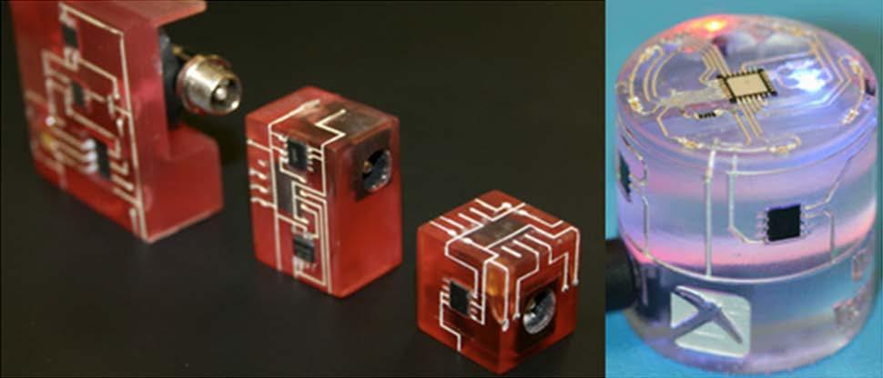
9 WHAT ARE FLEXIBLE HYBRID ELECTRONICS? 6/13/2017 PAGE 8


10 WHY FHE? Flexible Stretchable Conformable Transparent Biocompatible Lightweight Cost Effective 6/13/2017 PAGE 9


11 CREATING AN INDUSTRY 6/13/


12 FHE INTEGRATION 6/13/
13 WHAT IS SO COMPELLING ABOUT ADDITIVE MANUFACTURING? 6/13/2017 PAGE 12


14 ADDITIVE ADVANTAGES Low Waste Inventory Alternatives Ability to Manufacture Features Impossible with Subtractive Methods Topics Digital Process Flow In Situ Process Metrology and Adjustment Cost Effective for High Mix Low Volume Turner s Cube vs. 6/13/2017 PAGE 13


15 FUNCTIONAL MASS CUSTOMIZATION Additive methods lend themselves to digital process flow This means high mix low volume can be achieved cost effectively


16 3D Printing Functional Systems SIMPLE CO-DEPOSITED ELECTRONICS 6/13/2017 PAGE 15


17 RIGID & PLANAR PCB PRINTERS 6/13/2017 PAGE 16 16
18 FHE APPLICATIONS 6/13/2017 PAGE 17


19 PC 1.0: Die Integration to Stretchable Substrates TEXTILE INTEGRATED ICs 6/13/2017 PAGE 18


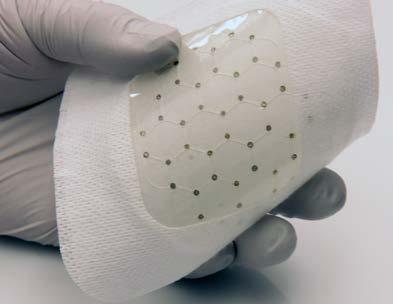
20 OXYGEN MANAGEMENT FOR WOUNDS 6/13/2017 PAGE 19


 110 100 90 80 70 60 50 40")
 -Working")

21 ORAL BIOCHEMISTRY Overall Objective(s) & Duration: Deliver flexible mouth guard senor label with wireless charging and readout Develop semi-automated flexhybrid manufacturing method Duration 16 months I normalized (%) PB-H2O2-Buffer PB-BSA-H2O2-Buffer t (min) -Working electrode(s): Prussian Blue (PB)/Carbon (C) -Counter electrode: PB/C -Reference electrode: Ag/AgCl 6/13/2017 PAGE 20


22 WIRELESS ECG Data Measured by GE at 10GHz Sample Type Dk Df Fused Silica Corning XG Glass Upliex 125SSDB Kapton E Kapton H Kapton HN Ultem Ultem Mylar Flex-Only Modules ECG Interface A/D In order to determine nominal RF properties of the base substrate materials GE utilized its 10GHz NIST provided Re- Entrant Cavity (optimized for thin film (1 to 5 mil) testing) Flex-Stretch Zones Pwr Mgmt Batt 6/13/2017 PAGE 21


23 FHE CYLINDRICAL X-BAND Objective Demonstrate FHE x-band array Benefits Flexible and conformal enables manufacture of single array to cover 360 Lower cost thru installation of single array, reduced maintenance costs with no moving parts, and manufacture on flex Improved performance over dish antenna with faster scan rate Approach Leverage team s key technologies: SI2 s printed phased array UML s printed electronics components Raytheon s low-cost T/R modules 6/13/2017 PAGE 22 22


24 SOFT ROBOTICS 6/13/2017 PAGE 23
25 MANUFACTURING FHE 6/13/2017 PAGE 24


26 FHE BUILDING BLOCKS Strain Gage Printed Battery Printed Antenna Die Placement Trace Print CMOS Radio Integrated Si Die Stretch Conductor Integration & Lamination Antenna Print Skin Contact Die on Stretch Die Thinning 6/13/2017 PAGE 25
27 FHE BUILDING BLOCKS Strain Gage Printed Battery Sensor Printed Antenna Processor Die Placement Trace Print Memory CMOS Radio Integrated Si Die Power Stretch Conductor Transceiver Integration & Lamination Antenna Print Application Specific Package Skin Contact Die on Stretch Die Thinning 6/13/2017 PAGE 26


28 FLEX ARDUINO PROJECT 6/13/2017 PAGE 27

![thick Si die Probability of survival [%] 99 90 80 70 60 50 40 30 20 10 5 3](/docs-images/89/98844054/images/29-1.jpg "2 The thinner the die, the smaller the bend radius is: 1 0.9 1 1.")
![5 2 Min bend radius [mm] 3 4 5 Thickness 35μm 25μm 15μm 6 7 however, the](/docs-images/89/98844054/images/29-3.jpg "flex substrate also matters: 12mm ROC Here is why the FHE dies need to be")
29 ULTRATHIN DIE The semiconductor die must be thinner than 50 μm to be flexible 25µm thick ultra-thin silicon die: 25 μm thick Si die 250 μm thick Si die Probability of survival [%] The thinner the die, the smaller the bend radius is: Min bend radius [mm] Thickness 35μm 25μm 15μm 6 7 however, the flex substrate also matters: 12mm ROC Here is why the FHE dies need to be thin: 6/13/2017 PAGE 28
 Adhesive bonding vs.")


 CMOS at the")
30 THE IMPORTANCE OF NEUTRAL PLANE Standalone die CoF (Chip on Flex) Adhesive bonding vs. soldering position of neutral plane σσ xxmax = pppp rr mmmmmm pp = tt dddddd 2 pp = tt ssssss bb, where bb = nn ii=1 EE ii tt ii ii jj=1 tt dddddd tt jj tt ii 2 nn ii=1 EE ii tt ii bb is always less than 2, can be negative Bonding methods affect the neutral plane position CiF (Chip in Flex) CMOS at the neutral plane 6/13/2017 PAGE 29

 Wirebonding: thickness,")


31 IC ASSEMBLY TECHNIQUES: FACE-UP OR FACE-DOWN? Face-up Face-down (adhesive bonding) Wirebonding: thickness, bonding force Anthony Leonardo, HHMI Janelia Farm Research Campus Uniqarta, Inc Isoplanar/direct write: reliability, curing, step American Semiconductor Flat Panel Display Materials - Trends and Forecasts 2009 Edition Adhesive flip-chip bonding is a mature technology 6/13/2017 PAGE 30


32 INTEGRATION OF SILICON ICA Conductive Adhesive Solder ACF/ACP Thermo-Compression TLPS Materials Direct Print 6/13/2017 PAGE 31


33 PRINTING METHODS Aerosol Jet Digital Extrusion Screen Rotogravure 6/13/2017 PAGE 32
34 PRINT METHODS Printing Method Contact Dynamic Dry film Resolution viscosity η thickness range limits DoD Ink jet No 1-20 cp µm 20/50 µm Aerosol jet No cp µm 10/50 µm Digital dispensing No 1-1M cp µm 20/50 µm Screen (PTF inks) Yes 1K-300K cp 5-15 µm 20/75 µm Flexographic (nano) Yes cp µm 5/25 µm Gravure Yes cp µm 20/50 µm Offset Gravure (pad) Yes cp µm 5/30 µm Offset Lithographic Yes 40k - 100k cp µm 10/50 µm Letterpress Yes 50K - 150K cp µm 10/25 µm Viscosity impacts aspect ratio for printed traces 6/13/2017 PAGE 33


35 CONDUCTOR PERFORMANCE (BY CLASS) 6/13/2017 PAGE 34


36 FHE PROCESS TOOLS FOR DEVICE INTEGRATION Conductor Printing & Curing Interconnect and Antenna Printing Component Placement Die Attachment 6/13/
37 DIGITAL PROCESS FLOW 6/13/2017 PAGE 36


38 DESIGN FLOW Product Definition/ Schematic Netlist Design/Layout/ Analysis Layout (Gerber File),BOM Manufacturing/Test Courtesy: American Semiconductor Arduino is registered trademark of Arduino 6/13/2017 PAGE 37
39 DESIGN DATA FILES Illustrator has not z-axis data Gerber has no part data Gerber Parts List/BOM NetList 6/13/2017 PAGE 38


40 PRINTED CIRCUIT ELEMENTS Resistor Diode Transistor Capacitor Source IMEC/HPE Source: Stratasys Source: PolyIC 6/13/ Source: Heraeus Source: Wiley Printed and organicelectronics 6/13/

41 DESIGN RULE CHECK 40 6/13/2017 PAGE 40 40

42 LAYOUT AND SCHEMATIC CAPTURE 6/13/2017 PAGE 41 41

43 DRC FOR PRINTED COMPONENTS 42 6/13/2017 PAGE 42 42
ring resonators Spiral")


44 RF TEST OF PRINT VS BULK COPPER Element Types on RF Test Frame Microstriplines Grounded coplanar line Filters (BPF)ring resonators Spiral inductors Fabrication: Duplicate Designs 1.Copper plate one version 2.Print Design element overlapping with launches Green =plated, Blue = printed S-parameters of coplanar waveguide printed and copper lines with HFSS simulations. Again, mode conversion is evident at the higher frequencies. 6/13/2017 PAGE 43
45 MRL AND TRL Definitional Material Solution Analysis Technology Development & Commercial Merit Engineering & Manufacturing Development MRL 1 Mfg feasibility assessed MRL 2 Mfg concepts defined MRL 3 Proof of Mfg concept MRL 4 Breadboard & manufacturing processes in a laboratory environment MRL 5 Breadboard & component manufacturing in a relevant environment MRL 6 Prototype, system & subsystem in production relevant environment MRL 7 Prototype, system & subsystem in operations and production environment MRL 8 Pilot line capability demonstrated; Ready to begin lowrate initial production MRL 9 Low-rate production demonstrated; capability in place to begin fullrate production 6/13/2017 PAGE 44


 Textile Wearables Lab Conf Break Room")
46 NEXTFLEX TECHNOLOGY HUB Lunch Room Conf Conf Conf Board Room Conf Lobby Seminar, Training and Workforce Development Design Lab Screen Exp Printing and Additive Processing Area (class 10,000 Clean Room) Materials Cubicles Product Display Materials Registry Library Test and Measurement Lab (class 10,000 Clean Room) Die Integration and Assembly Area (class 10,000 Clean Room) Textile Wearables Lab Conf Break Room 6/13/2017 PAGE 45

47 THANK YOU JASON MARSH CTO 6/13/2017 PAGE 46
Flexible Hybrid Electronics The Tipping Point To Drive Printed Electronics Market Growth
 Flexible Hybrid Electronics The Tipping Point To Drive Printed Electronics Market Growth November 7, 2016 Jason Marsh Director of Technology America s Flexible Hybrid Electronics Manufacturing Institute
Flexible Hybrid Electronics (FHE) Overview
 Overview") Flexible Hybrid Electronics (FHE) Overview in cooperation with NextFlex Manufacturing Institute Date: 12 March 2018 By: John Kornitsky CMTC-FHE Practice Lead @ NextFlex Mfg USA Institute Imagine... If
Flexible Hybrid Electronics (FHE) Overview in cooperation with NextFlex Manufacturing Institute Date: 12 March 2018 By: John Kornitsky CMTC-FHE Practice Lead @ NextFlex Mfg USA Institute Imagine... If
Flexible, Stretchable and Conformable Hybrid Electronics: Substrates and process considerations for building intelligent devices
 Flexible, Stretchable and Conformable Hybrid Electronics: Substrates and process considerations for building intelligent devices October 26, 2016 Jason Marsh Director of Technology America s Flexible Hybrid
Flexible Hybrid Electronics Fabricated with High-Performance COTS ICs using RTI CircuitFilm TM Technology
 Flexible Hybrid Electronics Fabricated with High-Performance COTS ICs using RTI CircuitFilm TM Technology Scott Goodwin 1, Erik Vick 2 and Dorota Temple 2 1 Micross Advanced Interconnect Technology Micross
NextFlex: Enabling a Domestic Manufacturing Ecosystem for Flexible Hybrid Electronics (Extended Abstract)
") NextFlex: Enabling a Domestic Manufacturing Ecosystem for Flexible Hybrid Electronics (Extended Abstract) Benjamin J. Leever*, Eric W. Forsythe + *Air Force Research Laboratory, 2179 12th St., B652/R122,
NextFlex: Enabling a Domestic Manufacturing Ecosystem for Flexible Hybrid Electronics (Extended Abstract) Benjamin J. Leever*, Eric W. Forsythe + *Air Force Research Laboratory, 2179 12th St., B652/R122,
Processes for Flexible Electronic Systems
 Processes for Flexible Electronic Systems Michael Feil Fraunhofer Institut feil@izm-m.fraunhofer.de Outline Introduction Single sheet versus reel-to-reel (R2R) Substrate materials R2R printing processes
Printed Electronics. Applications
 Printed Electronics Research Through University-Industry Partnerships Outline Background on Printed Electronics (PE) Corporate Partnerships Raytheon UMass Lowell Research Institute (RURI) Printed Electronics
MID Manufacturing Process.
 3D Aerosol Jet Printing An Emerging MID Manufacturing Process. Dr. Martin Hedges Neotech Services MTP, Nuremberg, Germany info@neotechservices.com Aerosol Jet Printing Aerosol Jet Process Overview Current
Printed Electronics and Additive Microelectronic Packaging For RF/Microwave Applications
 Printed Electronics and Additive Microelectronic Packaging For RF/Microwave Applications Prof. Craig Armiento University of Massachusetts Lowell Raytheon UMass Lowell Research Institute (RURI) Printed
Printed and Hybrid Integration
 Printed and Hybrid Integration Neil Chilton PhD Technical Director, Printed Electronics Limited, UK Neil.Chilton@PrintedElectronics.com Printed Electronics Limited (PEL) General Overview PEL was founded
Thin Film Resistor Integration into Flex-Boards
 Thin Film Resistor Integration into Flex-Boards 7 rd International Workshop Flexible Electronic Systems November 29, 2006, Munich by Dr. Hans Burkard Hightec H MC AG, Lenzburg, Switzerland 1 Content HiCoFlex:
NEXTFLEX WEBINAR PROJECT CALL 3.0
 NEXTFLEX WEBINAR PROJECT CALL 3.0 OVERVIEW and Q & A JUNE 8 2017 Agenda 2017FLEX Additional Resources NextFlex Background Process, Schedule, Themes PC 3.0 Topics Manufacturing Thrust Area (MTA) Topics
Application Bulletin 240
 Application Bulletin 240 Design Consideration CUSTOM CAPABILITIES Standard PC board fabrication flexibility allows for various component orientations, mounting features, and interconnect schemes. The starting
Integrated Photonics using the POET Optical InterposerTM Platform
 Integrated Photonics using the POET Optical InterposerTM Platform Dr. Suresh Venkatesan CIOE Conference Shenzhen, China Sept. 5, 2018 POET Technologies Inc. TSXV: PUBLIC POET PTK.V Technologies Inc. PUBLIC
NextFlex THE FLEXIBLE FUTURE OF ELECTRONICS. imaps New England 43rd Symposium & Expo May 03, 2016
 NextFlex THE FLEXIBLE FUTURE OF ELECTRONICS imaps New England 43rd Symposium & Expo May 03, 2016 America s Flexible Hybrid Electronics Manufacturing Institute Building a National Network of Institutes
!"#$"%&' ()#*+,-+.&/0(
#*+,-+.&/0(") !"#$"%&' ()#*+,-+.&/0( Multi Chip Modules (MCM) or Multi chip packaging Industry s first MCM from IBM. Generally MCMs are horizontal or two-dimensional modules. Defined as a single unit containing two
!"#$"%&' ()#*+,-+.&/0( Multi Chip Modules (MCM) or Multi chip packaging Industry s first MCM from IBM. Generally MCMs are horizontal or two-dimensional modules. Defined as a single unit containing two
NextFlex. Flexible Hybrid Electronics Manufacturing
 SPECIAL SECTION ADVANCED MANUFACTURING NextFlex Flexible Hybrid Electronics Manufacturing Eric Forsythe, Ph.D. n Benjamin J. Leever, Ph.D. N extflex, America s Flexible Hybrid Electronics Manufacturing
Accelerating Scale Up of Large Area Electronics
 Accelerating Scale Up of Large Area Electronics Duncan Lindsay Business Development Director, CPI 2015 Centre for Process Innovation Limited. All Rights Reserved. Who are CPI? CPI is a UK technology innovation
B. Flip-Chip Technology
 B. Flip-Chip Technology B1. Level 1. Introduction to Flip-Chip techniques B1.1 Why flip-chip? In the development of packaging of electronics the aim is to lower cost, increase the packaging density, improve
Lecture: Integration of silicon photonics with electronics. Prepared by Jean-Marc FEDELI CEA-LETI
 Lecture: Integration of silicon photonics with electronics Prepared by Jean-Marc FEDELI CEA-LETI Context The goal is to give optical functionalities to electronics integrated circuit (EIC) The objectives
RF circuit fabrication rules
 RF circuit fabrication rules Content: Single layer (ref. page 4) No vias (ref. page 4) With riveted vias (ref. pages 4,5,6) With plated vias (ref. pages 4, 5,7,8,9,10,11) Component assembly (ref. pages
University of Texas at Austin, Austin, TX ABSTRACT
 Phase Shifter using Carbon Nanotube Thin-Film Transistor for Flexible Phased-Array Antenna Daniel Pham 1, Harish Subbaraman 2, Maggie Yihong Chen 3, Xiaochuan Xu 1, and Ray T. Chen 1 1 Microelectronics
CMP for More Than Moore
 2009 Levitronix Conference on CMP Gerfried Zwicker Fraunhofer Institute for Silicon Technology ISIT Itzehoe, Germany gerfried.zwicker@isit.fraunhofer.de Contents Moore s Law and More Than Moore Comparison:
Novel Packaging Approaches for Miniature Antennas
 Novel Packaging Approaches for Miniature Antennas Will McKinzie, Greg Mendolia, and John Dutton Etenna Corporation 6100-C Frost Place, Laurel, MD 20707 wmckinzie@etenna.com, gmendolia@etenna.com, and jdutton@etenna.com
Flexible Glass Applications & Process Scaling
 Flexible Glass Applications & Process Scaling Sean Garner, Sue Lewis, Gary Merz, Alex Cuno, Ilia Nikulin October 16, 2017 Outline Flexible Glass Applications Process Scaling Summary 2 Flexible Glass Enables
MEMS in ECE at CMU. Gary K. Fedder
 MEMS in ECE at CMU Gary K. Fedder Department of Electrical and Computer Engineering and The Robotics Institute Carnegie Mellon University Pittsburgh, PA 15213-3890 fedder@ece.cmu.edu http://www.ece.cmu.edu/~mems
Georgia Tech. Greetings from. 3D Modeling and Process Design Kits for Flexible Hybrid Electronics (FHE) Challenges and Opportunities
 Challenges and Opportunities") Greetings from Georgia Tech 3D Modeling and Process Design Kits for Flexible Hybrid Electronics (FHE) Challenges and Opportunities Madhavan Swaminathan* and Sebastian Mueller John Pippin Chair in Electromagnetics
Greetings from Georgia Tech 3D Modeling and Process Design Kits for Flexible Hybrid Electronics (FHE) Challenges and Opportunities Madhavan Swaminathan* and Sebastian Mueller John Pippin Chair in Electromagnetics
shaping global nanofuture ULTRA-PRECISE PRINTING OF NANOMATERIALS
 shaping global nanofuture ULTRA-PRECISE PRINTING OF NANOMATERIALS WHO ARE WE? XTPL S.A. is a company operating in the nanotechnology segment. The interdisciplinary team of XTPL develops on a global scale
Z-Wrap-110 Loss 31 July 01
 Z-Wrap-11 Loss 31 July 1 Z-Axis J. Sortor TEST METHOD: To accurately measure complex impedance, it is required that the network analyzer be calibrated up to the phase plane of the unit under test (UUT).
1. Exceeding these limits may cause permanent damage.
 Silicon PIN Diode s Features Switch & Attenuator Die Extensive Selection of I-Region Lengths Hermetic Glass Passivated CERMACHIP Oxide Passivated Planar s Voltage Ratings to 3000V Faster Switching Speed
PAGE 1/6 ISSUE Jul SERIES Micro-SPDT PART NUMBER R516 XXX 10X R 516 _ 1 0 _
 PAGE 1/6 ISSUE Jul-24-2017 SERIES Micro-SPDT PART NUMBER R516 XXX 10X R516 series: the RAMSES concept merges with the SLIM LINE technology, breaking up the frequency limits of SMT switches : - FULL SMT
GLOBAL MARKETS, TECHNOLOGIES AND MATERIALS FOR THIN AND ULTRATHIN FILMS
 GLOBAL MARKETS, TECHNOLOGIES AND MATERIALS FOR THIN AND ULTRATHIN FILMS SMC057C August Margareth Gagliardi Project Analyst ISBN: 1-62296-338-5 BCC Research 49 Walnut Park, Building 2 Wellesley, MA 02481
ON-CHIP TECHNOLOGY INDEPENDENT 3-D MOD- ELS FOR MILLIMETER-WAVE TRANSMISSION LINES WITH BEND AND GAP DISCONTINUITY
 Progress In Electromagnetics Research B, Vol. 22, 171 185, 2010 ON-CHIP TECHNOLOGY INDEPENDENT 3-D MOD- ELS FOR MILLIMETER-WAVE TRANSMISSION LINES WITH BEND AND GAP DISCONTINUITY G. A. Wang, W. Woods,
Herzlich willkommen. Druckbare Sensoren für Food Packaging ICT-Agri-Food Symposium. Sören Fricke Section Head Large Area & Flexible Systems
 Herzlich willkommen Druckbare Sensoren für Food Packaging ICT-Agri-Food Symposium Sören Fricke Section Head Large Area & Flexible Systems Agroscope Tänikon, 05.09.2017 Motivation Printed Sensors can be
Chapter 2. Literature Review
 Chapter 2 Literature Review 2.1 Development of Electronic Packaging Electronic Packaging is to assemble an integrated circuit device with specific function and to connect with other electronic devices.
Advanced Packaging - Pulsed-laser Heating for Flip Chip Assembly
 Page 1 of 5 Pulsed-laser Heating for Flip Chip Assembly A stress-free alternative By Thorsten Teutsch, Ph.D., Pac Tech USA, Elke Zakel, Ph.D., and Ghassem Azdasht, Pac Tech GmbH As flip chip applications
Ultra-thin, highly flexible RF cables and interconnections
 Ultra-thin, highly flexible RF cables and interconnections Hans Burkard, Hightec MC AG, Lenzburg, Switzerland Urs Brunner, Hightec MC AG, Lenzburg, Switzerland Karl Kurz, Hightec MC AG, Lenzburg, Switzerland
Accelerating Collective Innovation: Investing in the Innovation Landscape
 PCB Executive Forum Accelerating Collective Innovation: Investing in the Innovation Landscape How a Major Player Uses Internal Venture Program to Accelerate Small Players with Big Ideas Dr. Joan K. Vrtis
National Centre for Flexible Electronics
 National Centre for Flexible Electronics Tripartite Partnership Government FlexE Centre - A platform for a meaningful interaction between industry and academia. An interdisciplinary team that advances
PAGE 1/6 ISSUE SERIES Micro-SPDT PART NUMBER R516 XXX 10X. (All dimensions are in mm [inches]) R 516 _ 1 0 _
![PAGE 1/6 ISSUE SERIES Micro-SPDT PART NUMBER R516 XXX 10X. (All dimensions are in mm [inches]) R 516 _ 1 0 _](/thumbs/96/127769340.jpg "PAGE 1/6 ISSUE SERIES Micro-SPDT PART NUMBER R516 XXX 10X. (All dimensions are in mm [inches]) R 516 _ 1 0 _") PAGE 1/6 ISSUE 15-10-18 SERIES Micro-SPDT PART NUMBER R516 XXX 10X R516 series: the RAMSES concept merges with the SLIM LINE technology, breaking up the frequency limits of SMT switches : - FULL SMT TECHNOLOGY
PAGE 1/6 ISSUE 15-10-18 SERIES Micro-SPDT PART NUMBER R516 XXX 10X R516 series: the RAMSES concept merges with the SLIM LINE technology, breaking up the frequency limits of SMT switches : - FULL SMT TECHNOLOGY
Specifications subject to change Packaging
 VCSEL Standard Product Packaging Options All standard products are represented in the table below. The Part Number for a standard product is determined by replacing the x in the column Generic Part Number
Low Temperature Integration of Thin Films and Devices for Flexible and Stretchable Electronics
 Low Temperature Integration of Thin Films and Devices for Flexible and Stretchable Electronics Pooran Joshi, Stephen Killough, and Teja Kuruganti Oak Ridge National Laboratory FIIW 2015 Displays and PV
David B. Miller Vice President & General Manager September 28, 2005
 Electronic Technologies Business Overview David B. Miller Vice President & General Manager September 28, 2005 Forward Looking Statement During the course of this meeting we may make forward-looking statements.
Integrated diodes. The forward voltage drop only slightly depends on the forward current. ELEKTRONIKOS ĮTAISAI
 1 Integrated diodes pn junctions of transistor structures can be used as integrated diodes. The choice of the junction is limited by the considerations of switching speed and breakdown voltage. The forward
Optimal design methodology for RF SiP - from project inception to volume manufacturing
 Optimal design methodology for RF SiP - from project inception to volume manufacturing Chris Barratt Insight SiP 905 rue Albert Einstein Valbonne France 06560 Outline RF SiP Technologies Design Methodology
Manufacturing Development of a New Electroplated Magnetic Alloy Enabling Commercialization of PwrSoC Products
 Manufacturing Development of a New Electroplated Magnetic Alloy Enabling Commercialization of PwrSoC Products Trifon Liakopoulos, Amrit Panda, Matt Wilkowski and Ashraf Lotfi PowerSoC 2012 CONTENTS Definitions
Ultra-Thin, Highly Flexible Cables and Interconnections for Low and High Frequencies
 Ultra-Thin, Highly Flexible Cables and Interconnections for Low and High Frequencies Hans Burkard a, Tobias Lamprecht b, Thomas Morf b, Bert Jan Offrein b, Josef Link a a Hightec MC AG, Fabrikstrasse,
Hot Topics and Cool Ideas in Scaled CMOS Analog Design
 Engineering Insights 2006 Hot Topics and Cool Ideas in Scaled CMOS Analog Design C. Patrick Yue ECE, UCSB October 27, 2006 Slide 1 Our Research Focus High-speed analog and RF circuits Device modeling,
ENERGY SCIENCES INC. EB COATING DEVELOPMENTS FOR GRAPHIC ARTS
 ENERGY SCIENCES INC. EB COATING DEVELOPMENTS FOR GRAPHIC ARTS WHAT IS EB? INNOVATIVE METHOD OF IMMEDIATELY DRYING INKS COATINGS ADHESIVES WITHOUT HEAT OR LIGHT. HOW DOES AN E-BEAM WORK? Ø FILAMENTS EMIT
insert link to the published version of your paper
 Citation Niels Van Thienen, Wouter Steyaert, Yang Zhang, Patrick Reynaert, (215), On-chip and In-package Antennas for mm-wave CMOS Circuits Proceedings of the 9th European Conference on Antennas and Propagation
INSIGHT SiP. RF System in Package, design methodology and practical examples of highly integrated systems
 INSIGHT SiP RF System in Package, design methodology and practical examples of highly integrated systems Chris Barratt Insight SiP Sophia Antipolis France 1 RF SiP Technologies PRD Design Methodology Initial
Flexible Near Field Communication Sensor Labels Built on a Printed Dopant Polysilicon TFT Platform
 Flexible Near Field Communication Sensor Labels Built on a Printed Dopant Polysilicon TFT Platform Soumya Krishnamoorthy, Ashish Shukla, Mao Takashima, Joey Li, Patricia Beck, Atul Wokhlu, Aditi Chandra
SHELLCASE-TYPE WAFER-LEVEL PACKAGING SOLUTIONS: RF CHARACTERIZATION AND MODELING
 SHELLCASE-TYPE WAFER-LEVEL PACKAGING SOLUTIONS: RF CHARACTERIZATION AND MODELING M Bartek 1, S M Sinaga 1, G Zilber 2, D Teomin 2, A Polyakov 1, J N Burghartz 1 1 Delft University of Technology, Lab of
High Efficient Heat Dissipation on Printed Circuit Boards. Markus Wille, R&D Manager, Schoeller Electronics Systems GmbH
 High Efficient Heat Dissipation on Printed Circuit Boards Markus Wille, R&D Manager, Schoeller Electronics Systems GmbH m.wille@se-pcb.de Introduction 2 Heat Flux: Q x y Q z The substrate (insulation)
Passive Direct Print Sensors
 Passive Wireless Sensor Technology Workshop June 6-7, 2012 Hyatt Regency, La Jolla, CA Passive Direct Print Sensors Mike Newton mnewton@nscrypt.com nscrypt Inc. Orlando, Florida University of Texas at
Modeling, Design, and Demonstration of 2.5D Glass Interposers for 16-Channel 28 Gbps Signaling Applications
 Modeling, Design, and Demonstration of 2.5D Glass Interposers for 16-Channel 28 Gbps Signaling Applications Brett Sawyer, Bruce C. Chou, Saumya Gandhi, Jack Mateosky, Venky Sundaram, and Rao Tummala 3D
Application Note 5011
 MGA-62563 High Performance GaAs MMIC Amplifier Application Note 511 Application Information The MGA-62563 is a high performance GaAs MMIC amplifier fabricated with Avago Technologies E-pHEMT process and
Trends in RF/Microwave & High Speed Digital and their effect on PCB Technology Requirements
 Trends in RF/Microwave & High Speed Digital and their effect on PCB Technology Requirements Jim Francey Technical Service Manager The need for speed is satisfied by the delivery of high-speed broadband
Moving from R&D to Manufacture
 Moving from R&D to Manufacture NSF I/UCRC Annual Meeting January 9, 2014 Clara Asmail Senior Technical Advisor NIST MEP Agenda Overview of NIST MEP program Technology Acceleration and MEP s role Sampling
High efficient heat dissipation on printed circuit boards
 High efficient heat dissipation on printed circuit boards Figure 1: Heat flux in a PCB Markus Wille Schoeller Electronics Systems GmbH www.schoeller-electronics.com Abstract This paper describes various
EMERGING SUBSTRATE TECHNOLOGIES FOR PACKAGING
 EMERGING SUBSTRATE TECHNOLOGIES FOR PACKAGING Henry H. Utsunomiya Interconnection Technologies, Inc. Suwa City, Nagano Prefecture, Japan henryutsunomiya@mac.com ABSTRACT This presentation will outline
RIT. Printing. Project Goals. Printing Radio Frequency Identification (RFID) Tag Antennas Using Inks Containing Metal Nanoparticles
 Tag Antennas Using Inks Containing Metal Nanoparticles") Printing Radio Frequency Identification (RFID) Tag Antennas Using Inks Containing Metal Nanoparticles Bruce E. Kahn Rochester Institute of Technology bkahn@mail.rit.edu http://www.rit.edu/~bekpph/ RIT
Printing Radio Frequency Identification (RFID) Tag Antennas Using Inks Containing Metal Nanoparticles Bruce E. Kahn Rochester Institute of Technology bkahn@mail.rit.edu http://www.rit.edu/~bekpph/ RIT
LSI ON GLASS SUBSTRATES
 LSI ON GLASS SUBSTRATES OUTLINE Introduction: Why System on Glass? MOSFET Technology Low-Temperature Poly-Si TFT Technology System-on-Glass Technology Issues Conclusion System on Glass CPU SRAM DRAM EEPROM
Weii 2.4 GHz Ceramic Antenna Part no: SRCW004 ceriiant Product Specification
 Weii 2.4 GHz Ceramic Antenna Part no: SRCW004 ceriiant Product Specification 1. Features: 2.4GHz applications Bluetooth, WiFi, Zigbee, ISM. Ultra small ceramic chip solution. High Efficiency. SMD mounted.
Printed Electronics: success stories and future commercial applications
 Printed Electronics: success stories and future commercial applications Dr Guillaume Chansin @gchansin June 2017 Helping you profit from emerging technologies Advantages of printed electronics Mass production
Technology Overview. Blind Micro-vias. Embedded Resistors. Chip-on-flex. Multi-Tier Boards. RF Product. Multi-chip Modules. Embedded Capacitance
 Blind Micro-vias Embedded Resistors Multi-Tier Boards Chip-on-flex RF Product Multi-chip Modules Embedded Capacitance Technology Overview Fine-line Technology Agenda Corporate Overview Company Profile
Through Glass Via (TGV) Technology for RF Applications
 Technology for RF Applications") Through Glass Via (TGV) Technology for RF Applications C. H. Yun 1, S. Kuramochi 2, and A. B. Shorey 3 1 Qualcomm Technologies, Inc. 5775 Morehouse Dr., San Diego, California 92121, USA Ph: +1-858-651-5449,
Through Glass Via (TGV) Technology for RF Applications C. H. Yun 1, S. Kuramochi 2, and A. B. Shorey 3 1 Qualcomm Technologies, Inc. 5775 Morehouse Dr., San Diego, California 92121, USA Ph: +1-858-651-5449,
Hermetic Packaging Solutions using Borosilicate Glass Thin Films. Lithoglas Hermetic Packaging Solutions using Borosilicate Glass Thin Films
 Hermetic Packaging Solutions using Borosilicate Glass Thin Films 1 Company Profile Company founded in 2006 ISO 9001:2008 qualified since 2011 Headquarters and Production in Dresden, Germany Production
Application Note 5012
 MGA-61563 High Performance GaAs MMIC Amplifier Application Note 5012 Application Information The MGA-61563 is a high performance GaAs MMIC amplifier fabricated with Avago Technologies E-pHEMT process and
PERFORMANCE OF PRINTABLE ANTENNAS WITH DIFFERENT CONDUCTOR THICKNESS
 Progress In Electromagnetics Research Letters, Vol. 13, 59 65, 2010 PERFORMANCE OF PRINTABLE ANTENNAS WITH DIFFERENT CONDUCTOR THICKNESS A. K. Sowpati Department of Electronics & Computer Engineering Indian
Heterogeneous integration of autonomous smart films based on electrochromic transistors
 of autonomous smart films NEWSLETTER #5 www.smartwww.smart-ec.eu Objectives SMART-EC has finalized last August 2014; it aimed at the development of self-powered electrochromic (EC) display device with
Advanced High-Density Interconnection Technology
 Advanced High-Density Interconnection Technology Osamu Nakao 1 This report introduces Fujikura s all-polyimide IVH (interstitial Via Hole)-multi-layer circuit boards and device-embedding technology. Employing
The Future for Printed Electronics
 The Future for Printed Electronics Jon Helliwell National Centre for Printable Electronics 24 October, 2013 Copyright CPI 2013. All rights reserved What is Printed Electronics? Organic and printed electronics
Session 4: Mixed Signal RF
 Sophia Antipolis October 5 th & 6 th 2005 Session 4: Mixed Signal RF Technology, Design and Manufacture of RF SiP Chris Barratt, Michel Beghin, Insight SiP Insight SiP Summary Introduction Definition of
SiP packaging technology of intelligent sensor module. Tony li
 SiP packaging technology of intelligent sensor module Tony li 2016.9 Contents What we can do with sensors Sensor market trend Challenges of sensor packaging SiP technology to overcome challenges Overview
MGA GHz 3 V, 17 dbm Amplifier. Data Sheet. Features. Description. Applications. Surface Mount Package. Simplified Schematic
 MGA-853.1 GHz 3 V, 17 dbm Amplifier Data Sheet Description Avago s MGA-853 is an economical, easy-to-use GaAs MMIC amplifier that offers excellent power and low noise figure for applications from.1 to
Electronic-Photonic ICs for Low Cost and Scalable Datacenter Solutions
 Electronic-Photonic ICs for Low Cost and Scalable Datacenter Solutions Christoph Theiss, Director Packaging Christoph.Theiss@sicoya.com 1 SEMICON Europe 2016, October 27 2016 Sicoya Overview Spin-off from
Application Note 5026
 Surface Laminar Circuit (SLC) Ball Grid Array (BGA) Eutectic Surface Mount Assembly Application Note 5026 Introduction This document outlines the design and assembly guidelines for surface laminar circuitry
MICROFLEX Project: MEMS on New Emerging Smart Textiles/Flexibles
 MICROFLEX Project: MEMS on New Emerging Smart Textiles/Flexibles S Beeby, M J Tudor, R Torah, K Yang, Y Wei Dr Steve Beeby ESD Research Group Smart Fabrics 2011 5 th April 2011 Overview Introduce the MicroFlex
EU Research project proposals (call for Finnish companies)
") EU Research project proposals (call for Finnish companies) 11th EEMELI Workshop 29 th August 2012 Jukka Hast Research Professor VTT Technical Research Centre of Finland 04/10/2012 2 General ICT theme work
EU Research project proposals (call for Finnish companies) 11th EEMELI Workshop 29 th August 2012 Jukka Hast Research Professor VTT Technical Research Centre of Finland 04/10/2012 2 General ICT theme work
Analysis of Wet Coating Thickness Effect on Transparent Conductive Electrode Performance using Silver Nanowire
 Analysis of Wet Coating Thickness Effect on Transparent Conductive Electrode Performance using Silver Nanowire 2017. 04. 25 Seung-Hyun Lee, PhD Senior Researcher Dept. Printed Electronics Korea Institute
TCLAD: TOOLS FOR AN OPTIMAL DESIGN
 TCLAD: TOOLS FOR AN OPTIMAL DESIGN THINGS TO CONSIDER WHEN DESIGNING CIRCUITS Many factors come into play in circuit design with respect to etching, surface finishing and mechanical fabrication processes;
45nm Foundry CMOS with Mask-Lite Reduced Mask Costs
 This work is sponsored by the Air Force Research Laboratory (AFRL/RVSE) TPOC: Mr. Kenneth Hebert 45nm Foundry CMOS with Mask-Lite Reduced Mask Costs 25 October 2011 www.americansemi.com 2011 American Semiconductor,
New fabrication and packaging technologies for CMOS pixel sensors: closing gap between hybrid and monolithic
 New fabrication and packaging technologies for CMOS pixel sensors: closing gap between hybrid and monolithic Outline Short history of MAPS development at IPHC Results from TowerJazz CIS test sensor Ultra-thin
Operation of Microwave Precision Fixed Attenuator Dice up to 40 GHz
 Operation of Microwave Precision Fixed Attenuator Dice up to 40 GHz (AN-70-019) I. INTRODUCTION Mini-Circuits YAT-D-series MMIC attenuator dice (RoHS compliant) are fixed value, absorptive attenuators
Integration of Optoelectronic and RF Devices for Applications in Optical Interconnect and Wireless Communication
 Integration of Optoelectronic and RF Devices for Applications in Optical Interconnect and Wireless Communication Zhaoran (Rena) Huang Assistant Professor Department of Electrical, Computer and System Engineering
ISSCC 2006 / SESSION 10 / mm-wave AND BEYOND / 10.1
 10.1 A 77GHz 4-Element Phased Array Receiver with On-Chip Dipole Antennas in Silicon A. Babakhani, X. Guan, A. Komijani, A. Natarajan, A. Hajimiri California Institute of Technology, Pasadena, CA Achieving
Data Sheet. ACFF-1024 ISM Bandpass Filter ( MHz) Description. Features. Specifications. Functional Block Diagram.
 Description. Features. Specifications. Functional Block Diagram.") ACFF-124 ISM Bandpass Filter (241 2482 MHz) Data Sheet Description The Avago ACFF-124 is a miniaturized Bandpass Filter designed for use in the 2.4 GHz Industrial, Scientific and Medical (ISM) band. The
ACFF-124 ISM Bandpass Filter (241 2482 MHz) Data Sheet Description The Avago ACFF-124 is a miniaturized Bandpass Filter designed for use in the 2.4 GHz Industrial, Scientific and Medical (ISM) band. The
Thermal Cycling and Fatigue
 Thermal Cycling and Fatigue Gil Sharon Introduction The majority of electronic failures are thermo-mechanically related by thermally induced stresses and strains. The excessive difference in coefficients
Si Nano-Photonics Innovate Next Generation Network Systems and LSI Technologies
 Si Nano-Photonics Innovate Next Generation Network Systems and LSI Technologies NISHI Kenichi, URINO Yutaka, OHASHI Keishi Abstract Si nanophotonics controls light by employing a nano-scale structural
Fully Printed Conformal Antenna and Sensors on 3D Plastic, Ceramic, and Metallic Substrates. Mike O Reilly
 Fully Printed Conformal Antenna and Sensors on 3D Plastic, Ceramic, and Metallic Substrates Mike O Reilly imaps NE 2016 Antenna and sensor printing via Aerosol Jet Optomec has developed high volume 3D
TD-DEV V Technical Specification
 High-Efficiency MODULE Carrier Board TD-DEV-500-12V Technical Specification POWER SUPPLY TECHNOLOGY FEATURES Low profile 1U, 500W power supply High efficiency power supply Fully integrated with CPU control
Newsletter 3 June 2013
 Newsletter 3 June 2013 Introduction Contents of this issue Welcome to the third issue of the PASTA Newsletter! PASTA is a EC funded project within FP7. It s the PASTA project s ambition to bring both worlds,
Characterization of Printed Circuit Board Material & Manufacturing Technology for High Frequency
 As originally published in the IPC APEX EXPO Conference Proceedings. Characterization of Printed Circuit Board Material & Manufacturing Technology for High Frequency AT&S Leoben, Austria Oliver Huber 1,
87x. MGA GHz 3 V Low Current GaAs MMIC LNA. Data Sheet
 MGA-876 GHz V Low Current GaAs MMIC LNA Data Sheet Description Avago s MGA-876 is an economical, easy-to-use GaAs MMIC amplifier that offers low noise and excellent gain for applications from to GHz. Packaged
Hardware Design Considerations for MKW41Z/31Z/21Z BLE and IEEE Device
 NXP Semiconductors Document Number: AN5377 Application Note Rev. 2, Hardware Design Considerations for MKW41Z/31Z/21Z BLE and IEEE 802.15.4 Device 1. Introduction This application note describes Printed
Design of an Integrated OLED Driver for a Modular Large-Area Lighting System
 Design of an Integrated OLED Driver for a Modular Large-Area Lighting System JAN DOUTRELOIGNE, ANN MONTÉ, JINDRICH WINDELS Center for Microsystems Technology (CMST) Ghent University IMEC Technologiepark
User s Guide to. Centre for Materials for Electronics Technology Panchawati, Off Pashan Road, Pune September Version 2.
 User s Guide to Centre for Materials for Electronics Technology Panchawati, Off Pashan Road, Pune 411008 September 2013 Version 2.1 Contents 1 Designing of LTCC Structures and Design Rules... 01 1.1 Guidelines
End-of-line Standard Substrates For the Characterization of organic
 FRAUNHOFER INSTITUTe FoR Photonic Microsystems IPMS End-of-line Standard Substrates For the Characterization of organic semiconductor Materials Over the last few years, organic electronics have become
Manufacture and Performance of a Z-interconnect HDI Circuit Card Abstract Introduction
 Manufacture and Performance of a Z-interconnect HDI Circuit Card Michael Rowlands, Rabindra Das, John Lauffer, Voya Markovich EI (Endicott Interconnect Technologies) 1093 Clark Street, Endicott, NY 13760