Analysis of Wet Coating Thickness Effect on Transparent Conductive Electrode Performance using Silver Nanowire
|
|
|
- Loreen Lang
- 6 years ago
- Views:
Transcription


1 Analysis of Wet Coating Thickness Effect on Transparent Conductive Electrode Performance using Silver Nanowire Seung-Hyun Lee, PhD Senior Researcher Dept. Printed Electronics Korea Institute of Machinery and Materials, 171 Jang-Dong, Yuseong-Gu, Daejeon, , KOREA R2R Printed Electro-Mechanical System 1/29


2 Development Trends in Electronics Low-cost Ubiquitous Large area Flexibility Tomorrow Future Today Rigid flat display RFID Smart card E-paper Digital signage Disposable electronics Wearable electronics Deformable batteries Deformable display


3 Development Trends in Electronics : IoT, Wearable, Flexible era. Common characteristics IoT Smartpackage market Size Large -> Large area patterning Demand High -> Mass production Precision medium -> Several or tens of micron Price cheap -> Cheap process Flexibility -> Plastic or paper substrate Solar cell Solar cell market Roll printing system, Gravure printing, flexo printing, InkJet printing, screen printingmicro contact printing, pad printing, R2R printing system Flexible diaply Display market


4 Paradigm Shift in Manufacturing Process Photolithography Complex process Long production time High cost equipment Large material consumption Rigid substrates VS Printing process No vacuum deposition / No photolithography Simple process Applicable to various substrates Lower fabrication costs Mass production (R2R)
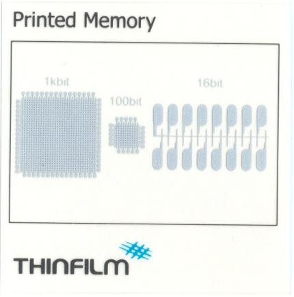
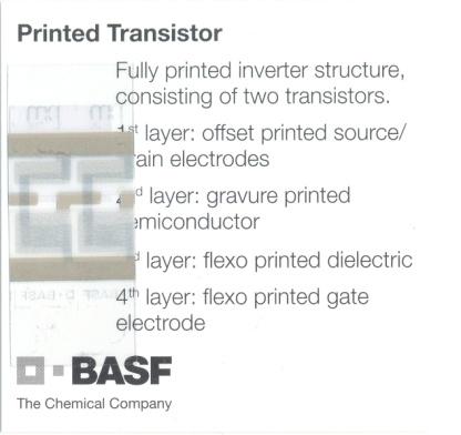
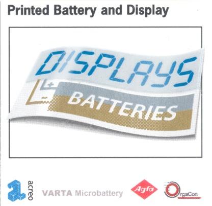
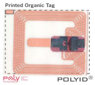
5 Applications of Printed Electronics Printed Memory Printed Transistor Printed Battery and Display Applications 활용분야 Printed Antenna Printed Solar Cell Printed RFID Tag Touch Screen <Ref :Oe-A>

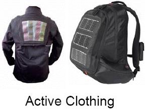

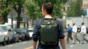
6 Applications of Printed Electronics Flexible Display Printed Solar Cell Portable Solar Cell RFID Tag Printed RFID Antenna
7 Dept. Printed KIMM History Personnel Topics Applications : abundant experiences over ten years in media printing processes and equipments : 35 full-time researchers related to printing technologies : mainly focused on printing processes and equipments (R2R gravure, Reverse-offset, Inkjet, ESD, Screen, Slot-die Coating, Micro-gravure Coating) : major research and development activities are oriented to industrial applications such as RFID tag, Solar cell(opv, CIGS), Touch screen panel, Supercapacitor, OLED, and Flexible display Materials Equipment Processin g & Analysis Functional electronic devices - Synthesis of NPs - E-ink (paste) formulation - Fine tuning for ink printability - Etc. - Reverse (offset) - (R2R) Gravure (offset) - (R2R) Slot-die coating - (R2R) Imprinting - Spin / Bar coating - Screen printing - Etc. - (R2R) IPL - (R2R) UV/NIR/MIR - (R2R) Plasma treatment - Multi-measurement system - UV-VIS spectroscopy - Solar simulator - Probe station - Etc. Development of large area & low cost electronics OPV / OLED / TFT / RFID / Sensors / Supercapacitor / Etc.


8 Dept. Printed KIMM Development of Roll-to-roll Printing Process & System Multi R2R Printing System (Gravure, Gravure-offset, Flexo Printing) Applications Touch screen panel, Color filter for LCD, E-paper, RFID, Solar cell, Flexible display etc. Low price & mass production of electronic devices. 96bit RFID antenna pattern with Ag nano ink


9 Dept. Printed KIMM Development of Roll-to-roll Coating Process & System R2R Slot-die Coating & Screen Printing System for OPV & TSP R2R Slot-die Coating System For Thin Film Supercapacitor Organic Solar Cells (Slot-die Coating & Screen Printing) Thin Film Supercapacitor


10 Dept. Printed KIMM Development of Roll-to-roll Imprinting Process & System R2R UV Imprinting System for Optical Film R2R Thermal Imprinting System for TCE


11 Dept. Printed KIMM MOU with PARC MOU with HP MOU with MGUP MOU with RISO MOU with Kent Univ.

12 Trend in TCE in Various Electronics

13 Trend in TCE in Various Electronics 13

14 Trend in TCE in Various Electronics


15 Trend in TCE in Various Electronics As is OLED Display Solar cell Based on glass (rigid) substrate / expensive material & process / To-be Deformable lightings Deformable displays Flexible, large area solar cells Wearable electronics Deformable battery + Multi-function (Integration)
 Brittle, Low Flexibility Market Needs Low Resistance : <30 Ω/sq High")

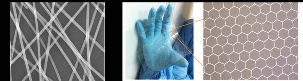
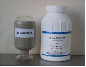
16 Trend in TCE in Various Electronics Problem of ITO High Resistance (>150 Ω/sq) Low Transparency (<87%) High Cost : Sputtering (>$80/ m2 ) Brittle, Low Flexibility Market Needs Low Resistance : <30 Ω/sq High Transparency : >89% Low Cost : R2R Wet Coating High Flexibility Need for New Flexible Transparent Conductive Electrode : High Performance AgNW TCE by R2R Coating ClearOhm TM Silver Nanowire Ref: Cambrios Website 23 LG V325 All-in-One PC
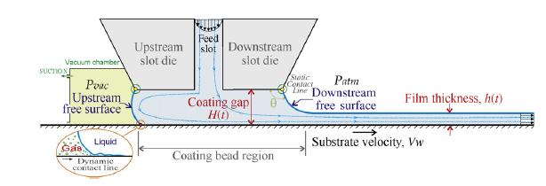
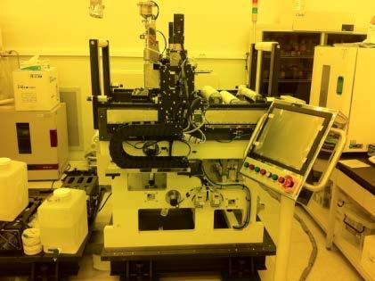
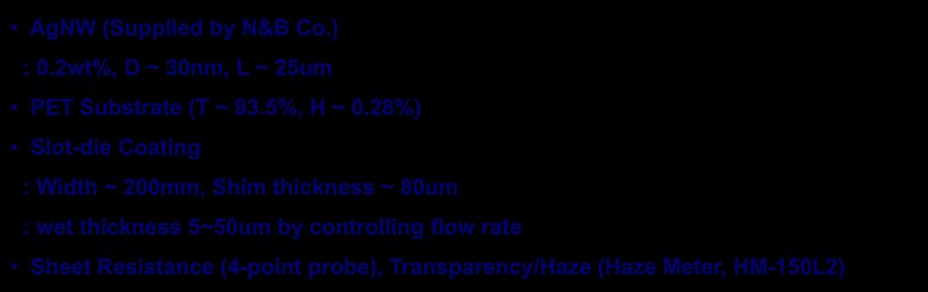
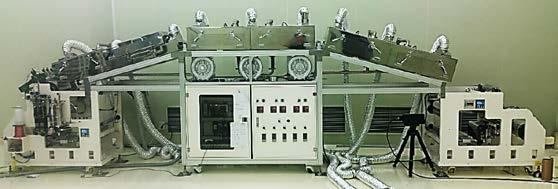
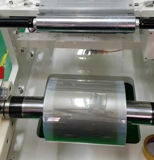
17 Experimental Details Ink Supply Wet film Substrate moving Schematic of Slot-die Coating Process Slot-die Coating System
 353 248 183 156 121 101 89.1 83.7 62.8 57.4 50.1 44.1 35.9 28.4 19.0 13.2 10.")

18 Experimental Results wet thickness , tw (um) Sheet Resistance, Rs (Ω/ ) Transparency, T (%) Haze, H (%) * Measured Transparency & Haze including substrate
 T Ag (%) 100 99 98 97 96 95 94 93 92 91 90 Rs (Ω/ ) 400.00 350.00 300.00 250.00 200.00 150.00 100.00 50")
19 Experimental Results T (%) Rs vs T Rs (Ω/ ) T Ag (%) Rs (Ω/ ) Rs (Ω/ ) H vs Rs H (%) T Ag is calculated transparency based on PET film (without PET)
20 Experimental Results T (%) 1-T Ag t w (um) t w (um) H Ag H(%) t w (um) t w (um)
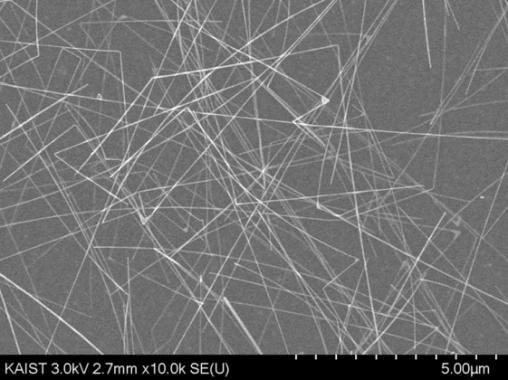
21 Experimental Results Rs (Ω/ ) Log(Rs) (Ω/ ) = 3600 wet R s t t w (um) 전도도 - 두께 Log(t w) (um) σ DC = 1 R s t film 1 R s t wet t 0.53 w Conductivity is not constatnt with film thickness : Transition (Network => Bulk) S. De et al. ACS Nano, 2009
22 Conclusions Pre-metered slot-die coating can easily control wet thickness of AgNW conductive film by changing web speed and flow rate Very high performance TCE were fabricated by using AgNW with high aspect ratio AgNW (T ~ 92%, Rs ~ 120Ω/, H < 1%) In range of Rs <10Ω/, conductivity is not constant due to percolation effect (σ DC ~ t 0.53 ) By controlling wet thickness of AgNW film, we can easily control and estimate the TCE performance such as sheet resistance, transparency and haze


23 Seung-Hyun Lee, PhD Senior Researcher Korea Institute of Machinery and Materials, 171 Jang-Dong, Yuseong-Gu, Daejeon, KOREA
National Centre for Flexible Electronics
 National Centre for Flexible Electronics Tripartite Partnership Government FlexE Centre - A platform for a meaningful interaction between industry and academia. An interdisciplinary team that advances
PRINTED ELECTRONICS 3
 PRINTED ELECTRONICS 3 4 INKTEC PRINTED ELECTRONICS 5 6 INKTEC PRINTED ELECTRONICS 7 InkTec Leads New Paradigm in Printed Electronic Materials Applications OTFT, Memory Cell, Display, RFID and so on Product
Printing versus coating technology Which way Printed Electronics with solution coating will go?
 Printing versus coating technology Which way Printed Electronics with solution coating will go? Frank Schäfer, Andrea Glawe, Dr. Daniel Eggerath, KROENERT GmbH& Co KG, Schuetzenstrasse 105, 22761 Hamburg
Reverse-offset Printing Process and Equipment for Fine Patterning and Precision Overlay
 Reverse-offset Printing Process and Equipment for Fine Patterning and Precision Overlay Dongwoo Kang (Ph.D) June 22, 2017 (Monterey) Korea Institute of Machinery & Materials (KIMM) Demand on FPE What is
The Future for Printed Electronics
 The Future for Printed Electronics Jon Helliwell National Centre for Printable Electronics 24 October, 2013 Copyright CPI 2013. All rights reserved What is Printed Electronics? Organic and printed electronics
Printable, Novel CNT Inks with V2V Technology
 Printable, Novel CNT Inks with V2V Technology William J. Hurley, Jr., PhD Chasm Technologies, Inc. Canton, MA June 23, 2010 New England Nanomanufacturing Summit 1 Outline CHASM Overview Alliance with SWeNT
GLOBAL MARKETS, TECHNOLOGIES AND MATERIALS FOR THIN AND ULTRATHIN FILMS
 GLOBAL MARKETS, TECHNOLOGIES AND MATERIALS FOR THIN AND ULTRATHIN FILMS SMC057C August Margareth Gagliardi Project Analyst ISBN: 1-62296-338-5 BCC Research 49 Walnut Park, Building 2 Wellesley, MA 02481
Optimization of Reverse Offset Roll to Plate (RO-R2P) Through Contact Angle
 Through Contact Angle") Optimization of Reverse Offset Roll to Plate (RO-R2P) Through Contact Angle Ji-Hyun Hwang, Kayna Lee Mendoza, Kyungdeok Jang, Seyeon Hwang, Namsoo Kim * Department of Metallurgy and Materials Engineering,
Optimization of Reverse Offset Roll to Plate (RO-R2P) Through Contact Angle Ji-Hyun Hwang, Kayna Lee Mendoza, Kyungdeok Jang, Seyeon Hwang, Namsoo Kim * Department of Metallurgy and Materials Engineering,
Flexible Glass Applications & Process Scaling
 Flexible Glass Applications & Process Scaling Sean Garner, Sue Lewis, Gary Merz, Alex Cuno, Ilia Nikulin October 16, 2017 Outline Flexible Glass Applications Process Scaling Summary 2 Flexible Glass Enables
Processes for Flexible Electronic Systems
 Processes for Flexible Electronic Systems Michael Feil Fraunhofer Institut feil@izm-m.fraunhofer.de Outline Introduction Single sheet versus reel-to-reel (R2R) Substrate materials R2R printing processes
Accelerating Scale Up of Large Area Electronics
 Accelerating Scale Up of Large Area Electronics Duncan Lindsay Business Development Director, CPI 2015 Centre for Process Innovation Limited. All Rights Reserved. Who are CPI? CPI is a UK technology innovation
Plastic Electronics Market Development. by Mr. Ed van den Kieboom Executive Board Member Plastic Electronics Foundation
 Plastic Electronics Market Development by Mr. Ed van den Kieboom Executive Board Member Plastic Electronics Foundation Plastic Electronics Foundation Established April 2005 Private non profit organization
ORGANIC ELECTRONICS: PHOTOLITHOGRAPHY OR PRINTING. Giles Lloyd Flex Europe Conference, 25th October 2016
 ORGANIC ELECTRONICS: PHOTOLITHOGRAPHY OR PRINTING Giles Lloyd Flex Europe Conference, 25th October 2016 Organic Electronics: Photoligthography or Printing? Lithography Printing Enabling flexible TFT sheet-fed
Supplementary Information
 Supplementary Information Wireless thin film transistor based on micro magnetic induction coupling antenna Byoung Ok Jun 1, Gwang Jun Lee 1, Jong Gu Kang 1,2, Seung Uk Kim 1, Ji Woong Choi 1, Seung Nam
AGC Glass Technology Solution to Highly Functional Display Needs
 AGC Glass Technology Solution to Highly Functional Display Needs Takahiro IKEZAKI Vice President Electronics Glass General Division, AGC Electronics, Asahi Glass Co., Ltd. June 5, 2012 -Contents- AGC Strengths
Low Temperature Integration of Thin Films and Devices for Flexible and Stretchable Electronics
 Low Temperature Integration of Thin Films and Devices for Flexible and Stretchable Electronics Pooran Joshi, Stephen Killough, and Teja Kuruganti Oak Ridge National Laboratory FIIW 2015 Displays and PV
Large Area, Flexible Electronics TWG. Chair: Dan Gamota, Jabil
 Large Area, Flexible Electronics TWG Chair: Dan Gamota, Jabil Large Area Flexible Electronics Roadmap History 09/2005 inemi Stakeholders identify Flexible Electronics as Future Growth Market and authorize
Context Development Details Anticipated Effects
 Dec 27, 2017 Tanaka Precious Metals/Tanaka Holdings Co., Ltd Japan Science and Technology Agency (JST). A Bendable Touch Panel Achieved with Silver Nano Ink Printing Technology (A Result of NexTEP: Joint
Single Layer Color Cholesteric Liquid Crystal Display
 Single Layer Color Cholesteric Liquid Crystal Display Frank Shiu jwshiu@itri.org.tw Tel:886-35915562 Display Technology Center Industrial Technology Research Institute Taiwan, R.O.C. 1 Outline Applications
Flexible glass substrates for roll-to-roll manufacturing
 Science & Technology Flexible glass substrates for roll-to-roll manufacturing Corning - S. Garner, G. Merz, J. Tosch, C. Chang, D. Marshall, X. Li, J. Matusick, J. Lin, C. Kuo, S. Lewis, C. Kang ITRI -
Printed Electronics - Quo Vadis? What is Printed Electronics et Quo Vadis?
 Printed Electronics - Quo Vadis? Emil J.W. List Institute of Solid State Physics Graz University of Technology NanoTecCenter Weiz Forschungsgesellschaft mbh Agenda Introduction Motivation What is Printed
Printed Electronics: success stories and future commercial applications
 Printed Electronics: success stories and future commercial applications Dr Guillaume Chansin @gchansin June 2017 Helping you profit from emerging technologies Advantages of printed electronics Mass production
Yamagata University Organic Thin Film Device Consortium
 Innovation Center for Organic Electronics Greeting Participating Companies (Jan. 2016) Yamagata University Organic Thin Film Device Consortium [*] has developed Flexible Substrates with Alternative Electrode
Henkel solutions enabling printed electronics. Dr. Crystal Yang
 Henkel solutions enabling printed electronics Dr. Crystal Yang Agenda 1. Introduction Henkel 2. Trends in Printed Electronics 3. Novel materials enabling Printed Electronics New high speed printable silver
 Organic and flexible Electronics in Saxony www.invest-in-saxony.com WElCOME Organic electronics are based on the discovery that specific organic materials possess semiconducting properties. Functional
Micro-PackS, Technology Platform. Security Characterization Lab Opening
 September, 30 th 2008 Micro-PackS, Technology Platform Security Characterization Lab Opening Members : Micro-PackS in SCS cluster From Silicium to innovative & commucating device R&D structure, gathering
shaping global nanofuture ULTRA-PRECISE PRINTING OF NANOMATERIALS
 shaping global nanofuture ULTRA-PRECISE PRINTING OF NANOMATERIALS WHO ARE WE? XTPL S.A. is a company operating in the nanotechnology segment. The interdisciplinary team of XTPL develops on a global scale
Photo-patternable and Transparent Films Using Cellulose Nanofibers for Stretchable, Origami Electronics
 Supplementary information for Photo-patternable and Transparent Films Using Cellulose Nanofibers for Stretchable, Origami Electronics Sangyoon Ji 1, 4, Byung Gwan Hyun 1, 4, Kukjoo Kim 1, 4, Sang Yun Lee
Здра вствуйте, това рищи!
 Manufacturing of Smart Objects by Printing Technologies Здра вствуйте, това рищи! Moscow / RUS, June 05, 2013 Reinhard R. Baumann Chemnitz University of Technology Chair of Digital Printing Fraunhofer
Flexible Electronics: Revolutionary Products and Career Opportunities for Creative Engineers
 Flexible Electronics: Revolutionary Products and Career Opportunities for Creative Engineers TAPPI - PIMA Student Summit 2011 Michael Ciesinski President January 15, 2011 Microelectronics changed the world
PILOT LINE FOR LARGE-AREA PRINTING OF ELECTRONIC AND PHOTONIC DEVICES. Simon Perraud, Ph.D. Vice president for European affairs
 PILOT LINE FOR LARGE-AREA PRINTING OF ELECTRONIC AND PHOTONIC DEVICES Simon Perraud, Ph.D. Vice president for European affairs ABOUT LITEN Liten is the research institute of CEA devoted to clean energy
Supplementary Information. Highly conductive and flexible color filter electrode using multilayer film
 Supplementary Information Highly conductive and flexible color filter electrode using multilayer film structure Jun Hee Han 1, Dong-Young Kim 1, Dohong Kim 1, and Kyung Cheol Choi 1,* 1 School of Electrical
Printable Electronics
 Printable Electronics Printable Electronics The Centre for Process Innovation From innovation to commercialisation The Centre for Process Innovation From innovation to commercialisation The High Value
2007-Novel structures of a MEMS-based pressure sensor
 C-(No.16 font) put by office 2007-Novel structures of a MEMS-based pressure sensor Chang-Sin Park(*1), Young-Soo Choi(*1), Dong-Weon Lee (*2) and Bo-Seon Kang(*2) (1*) Department of Mechanical Engineering,
High Performance Silver Nanowire based Transparent Electrodes Reinforced by Conductive Polymer Adhesive
 High Performance Silver Nanowire based Transparent Electrodes Reinforced by Conductive Polymer Adhesive Qisen Xie, Cheng Yang*, Zhexu Zhang, Ruobing Zhang Division of Energy and Environment, Graduate School
Supporting Information. A Tough and High-Performance Transparent Electrode from a. Scalable Transfer-Free Method
 Supporting Information A Tough and High-Performance Transparent Electrode from a Scalable Transfer-Free Method Tianda He, Aozhen Xie, Darrell H. Reneker and Yu Zhu * Department of Polymer Science, College
Heterogeneous integration of autonomous smart films based on electrochromic transistors
 of autonomous smart films NEWSLETTER #5 www.smartwww.smart-ec.eu Objectives SMART-EC has finalized last August 2014; it aimed at the development of self-powered electrochromic (EC) display device with
RIT. Printing. Project Goals. Printing Radio Frequency Identification (RFID) Tag Antennas Using Inks Containing Metal Nanoparticles
 Tag Antennas Using Inks Containing Metal Nanoparticles") Printing Radio Frequency Identification (RFID) Tag Antennas Using Inks Containing Metal Nanoparticles Bruce E. Kahn Rochester Institute of Technology bkahn@mail.rit.edu http://www.rit.edu/~bekpph/ RIT
Printing Radio Frequency Identification (RFID) Tag Antennas Using Inks Containing Metal Nanoparticles Bruce E. Kahn Rochester Institute of Technology bkahn@mail.rit.edu http://www.rit.edu/~bekpph/ RIT
Bayer MaterialScience Functional Films: Printed Polymer Electronics
 Bayer MaterialScience Functional Films: Printed Polymer Electronics Dr. Karsten Dierksen Bayer MaterialScience Head of Functional Films Printed Electronics & Functional Materials D-51368 Leverkusen, Tel.
Printing Beyond Color. Printed Smart Objects on Advanced Paper Substrates. Reinhard R. Baumann
 Printing Beyond Color Printed Smart Objects on Advanced Paper Substrates June 17, 2009 member of Reinhard R. Baumann member of Chemnitz University of Technology Institute for Print and Media Technology
Goals. Printable Electronics at R I T. Printing Methods. How do you print circuits?
 Goals at R T Design and print test patterns and antennas for applications Determine printing process capabilities for printing devices Study physical and electrical properties of printed features Fabricate
Flexible Hybrid Electronics Fabricated with High-Performance COTS ICs using RTI CircuitFilm TM Technology
 Flexible Hybrid Electronics Fabricated with High-Performance COTS ICs using RTI CircuitFilm TM Technology Scott Goodwin 1, Erik Vick 2 and Dorota Temple 2 1 Micross Advanced Interconnect Technology Micross
Saxony the Organic Electronics State
 Saxony the Organic Electronics State Page 1 Agenda 1. History 2. The situation today: a major cluster in Europe 3. Saxony a dynamic place to be 4. OES at your service 5. Why to join Page 2 Downtown Dresden
Additional information Indium-free, highly transparent, flexible Cu2O/Cu/Cu2O mesh electrodes for flexible touch screen panels
 Additional information Indium-free, highly transparent, flexible Cu2O/Cu/Cu2O mesh electrodes for flexible touch screen panels By Don-Ju Kim 1, Hyo-Joong Kim 1, Ki-Won Seo 1, Ki-Hyun Kim 2, Tae-Wong Kim
Pattern Coating by Slot-Die SCOTT A. ZWIERLEIN FRONTIER INDUSTRIAL TECHNOLOGY, INC. AIMCAL FALL TECHNICAL CONFERENCE 2013
 Pattern Coating by Slot-Die SCOTT A. ZWIERLEIN FRONTIER INDUSTRIAL TECHNOLOGY, INC. AIMCAL FALL TECHNICAL CONFERENCE 2013 Program: Slot-Die Coating Overview Industries for slot-die coating Stripe coating
Nanoimprint lithography with a focused laser beam for the fabrication of micro-/nano-hybrid patterns
 Supplementary Material (ESI) for Lab on a Chip This journal is The Royal Society of Chemistry 20XX Nanoimprint lithography with a focused laser beam for the fabrication of micro-/nano-hybrid patterns Hyungjun
All-Glass Gray Scale PhotoMasks Enable New Technologies. Che-Kuang (Chuck) Wu Canyon Materials, Inc.
 Wu Canyon Materials, Inc.") All-Glass Gray Scale PhotoMasks Enable New Technologies Che-Kuang (Chuck) Wu Canyon Materials, Inc. 1 Overview All-Glass Gray Scale Photomask technologies include: HEBS-glasses and LDW-glasses HEBS-glass
All-Glass Gray Scale PhotoMasks Enable New Technologies Che-Kuang (Chuck) Wu Canyon Materials, Inc. 1 Overview All-Glass Gray Scale Photomask technologies include: HEBS-glasses and LDW-glasses HEBS-glass
High throughput ultra-long (20cm) nanowire fabrication using a. wafer-scale nanograting template
 nanowire fabrication using a. wafer-scale nanograting template") Supporting Information High throughput ultra-long (20cm) nanowire fabrication using a wafer-scale nanograting template Jeongho Yeon 1, Young Jae Lee 2, Dong Eun Yoo 3, Kyoung Jong Yoo 2, Jin Su Kim 2,
Supporting Information High throughput ultra-long (20cm) nanowire fabrication using a wafer-scale nanograting template Jeongho Yeon 1, Young Jae Lee 2, Dong Eun Yoo 3, Kyoung Jong Yoo 2, Jin Su Kim 2,
OVERVIEW OF PLASTIC SUBSTRATES FOR PRINTED ELECTRONICS
 OVERVIEW OF PLASTIC SUBSTRATES FOR PRINTED ELECTRONICS Robert Rus:n Sr. Applica+on and Market Development Manager Special thanks to: Karl Rakos Bill MacDonald Melinex polyester film Mylar polyester film
Herzlich willkommen. Druckbare Sensoren für Food Packaging ICT-Agri-Food Symposium. Sören Fricke Section Head Large Area & Flexible Systems
 Herzlich willkommen Druckbare Sensoren für Food Packaging ICT-Agri-Food Symposium Sören Fricke Section Head Large Area & Flexible Systems Agroscope Tänikon, 05.09.2017 Motivation Printed Sensors can be
Ubiquitous Displays and Sensors Activating Surfaces with Flexible Electronics. Dean Baker, Director FlexEnable. APAC Innovation Summit 2016, Hong Kong
 Ubiquitous Displays and Sensors Activating Surfaces with Flexible Electronics Dean Baker, Director FlexEnable, Hong Kong Activating surfaces with flexible displays and sensors Flexible Plastic Displays
Supporting Information
 Supporting Information Highly Stretchable and Transparent Supercapacitor by Ag-Au Core Shell Nanowire Network with High Electrochemical Stability Habeom Lee 1, Sukjoon Hong 2, Jinhwan Lee 1, Young Duk
The Coating Machinery Experts
 The Coating Machinery Experts The Coating Machinery Experts Coating and printing processes for the surface functionalization newest developments in coating and lamination for specialty films and flexible
Flexible 2-Layer Paper Printed Circuit Board Fabricated by Inkjet Printing for 3-D Origami Electronics
 INTERNATIONAL JOURNAL OF PRECISION ENGINEERING AND MANUFACTURING-GREEN TECHNOLOGY Vol. 5, No. 3, pp. 421-426 JULY 2018 / 421 REGULAR PAPER DOI: 10.1007/s40684-018-0045-2 ISSN 2288-6206 (Print) / 2198-0810
UV-LED PRINTER SIMPLE & PERFECT
 UV-LED PRINTER SIMPLE & PERFECT JETRIX ULTRA HIGH SPEED UV LED PRINTER - 3.2m wide flatbed with ultra high printing speed and UV LED curing system InkTec s JETRIX production printer has a 3.2 x 2m wide
Session 9.1 SID2010 May 25 th, Sep Lyu Jae Jin. Samsung Electronics
 Session 9.1 SID2010 May 25 th, 2010 Sep. 18. 2010 Lyu Jae Jin Samsung Electronics Contents 2 Application of LCDs Projection Type: LCD Projector, Projection TV Direct View Type: Smart-Phone, I-Pad, N-PC,
Silver nanowire transparent electrodes. for device applications
 Silver nanowire transparent electrodes for device applications by Hadi Hosseinzadeh Khaligh A thesis presented to the University of Waterloo in fulfillment of the thesis requirement for the degree of Doctor
Effect of Corona Treatment on Spreading Behavior of UV Ink over Inkjet Printed Silver Nano-Particle Layer
 Effect of Corona Treatment on Spreading Behavior of UV Ink over Inkjet Printed Silver Nano-Particle Layer Khushbeen Department of Printing Technology GJUS&T, Hisar, Haryana, India Email- khushveen12@gmail.com
The Department of Advanced Materials Engineering. Materials and Processes in Polymeric Microelectronics
 The Department of Advanced Materials Engineering Materials and Processes in Polymeric Microelectronics 1 Outline Materials and Processes in Polymeric Microelectronics Polymeric Microelectronics Process
EMERGING INKJET PRINTING TECHNOLOGIES, APPLICATIONS AND GLOBAL MARKETS
 EMERGING INKJET PRINTING TECHNOLOGIES, APPLICATIONS AND GLOBAL MARKETS AVM091B November 2014 Andrew McWilliams Project Analyst ISBN: 1-56965-999-0 BCC Research 49 Walnut Park, Building 2 Wellesley, MA
Supplementary Figures
 Supplementary Figures Supplementary Figure 1 The diameter and length of AgNWs. (a) SEM image and (b) AFM image of AgNWs coated on a SiO2/Si wafer at 500 rpm for 30 sec. The diameter and length of the AgNWs
Introduction. Internet of things. Smart New World
 1 Introduction Internet of things Smart New World Source : iamwire IoT has evolved multiple technologies including sensors, embedded systems, communication, real-time analytics or machine learning. For
Contents. Contents. Preface... xi. PART A: OVERVIEW 1 Introduction... 1
 Contents Preface... xi PART A: OVERVIEW 1 Introduction... 1 1.1 Scope...1 1.2 Innovation and Patents...1 1.3 Prediction of Trends...1 1.4 Innovators...2 1.5 Comments on Presentation...3 1.5.1 Subject Classification...3
EU Research project proposals (call for Finnish companies)
") EU Research project proposals (call for Finnish companies) 11th EEMELI Workshop 29 th August 2012 Jukka Hast Research Professor VTT Technical Research Centre of Finland 04/10/2012 2 General ICT theme work
EU Research project proposals (call for Finnish companies) 11th EEMELI Workshop 29 th August 2012 Jukka Hast Research Professor VTT Technical Research Centre of Finland 04/10/2012 2 General ICT theme work
MoS 2 nanosheet phototransistors with thicknessmodulated
 Supporting Information MoS 2 nanosheet phototransistors with thicknessmodulated optical energy gap Hee Sung Lee, Sung-Wook Min, Youn-Gyung Chang, Park Min Kyu, Taewook Nam, # Hyungjun Kim, # Jae Hoon Kim,
3M Contrast Enhancement Film. The. Clear. Advantage. High purity, optical-grade adhesive films for joining transparent materials
 3M Contrast Enhancement Film The Clear Advantage High purity, optical-grade adhesive films for joining transparent materials 3 3M Contrast Enhancement Film Engineered to speed assembly, improve display
Making a Material Difference
 Making a Material Difference Founded as a QinetiQ corporate investment in January 2002 Spun out in 2007 Locations: Rochester, NYS, USA (HQ and Production) Farnborough and Malvern, UK (R&D, Production and
Digital Magnetics Support document
 Digital Magnetics Support document Digital Magnetics Change your graphics quickly. 01 / 02 Introduction DM 03 / 04 Support Ferro & Magnetic Base About DM 05 / 06 Support Flexible Ferrous films Digital
SUPPLEMENTARY INFORMATION
 A transparent bending-insensitive pressure sensor Sungwon Lee 1,2, Amir Reuveny 1,2, Jonathan Reeder 1#, Sunghoon Lee 1,2, Hanbit Jin 1,2, Qihan Liu 5, Tomoyuki Yokota 1,2, Tsuyoshi Sekitani 1,2,3, Takashi
LITE /LAB /SCAN /INLINE:
 Metis Metis LITE /LAB /SCAN/ INLINE Metis LITE /LAB /SCAN /INLINE: Spectral Offline and Inline Measuring System, using Integrating Sphere, for coatings on foils/web and on large size glasses To ensure
MID Manufacturing Process.
 3D Aerosol Jet Printing An Emerging MID Manufacturing Process. Dr. Martin Hedges Neotech Services MTP, Nuremberg, Germany info@neotechservices.com Aerosol Jet Printing Aerosol Jet Process Overview Current
ML² Multi Layer Micro Lab
 Deliverable 4.5 ML² Multi Layer Micro Lab D4.5 - Report on product range for UV curing lacquers, validated for ML² devices 1. Introduction... 2 2. UV embossing lacquer chemistry... 2 2.1. The main components
Advancing Consumer Packaging Through Printable Electronics
 IPST Executive Conference, Atlanta, GA March 9-10, 2011 Advancing Consumer Packaging Through Printable Electronics Bernard Kippelen Professor, School of Electrical and Computer Engineering Director, Center
Recent developments in PEDOT/PSS - Formulations and Ink for Printable Electrodes
 Recent developments in PEDOT/PSS - Formulations and Ink for Printable Electrodes Bavo Muys Application Manager ORGACON Electronic Materials T: +32-3-4442166 F: +32-3-4447662 M: +32-494-560 480 Bavo.muyst@agfa.com
Solution-Processed Metal Nanowire Mesh Transparent Electrodes
 Letter Subscriber access provided by STANFORD UNIV GREEN LIBR Solution-Processed Metal Nanowire Mesh Transparent Electrodes Jung-Yong Lee, Stephen T. Connor, Yi Cui, and Peter Peumans Nano Lett., 2008,
Obducat NIL 6. Nanoimprinting with NRF s NIL 6
 Obducat NIL 6 Substrates: pieces to 6 inch, hard or soft Thermal cure with PMMA, MR I 7010 etc Alignment to about 3 microns Temperature to 300 HC Pressure 15 to 80 bars Resolution < 50 nm possible Up to
Challenges and Requirements for Flexible Displays and Microelectronics
 Challenges and Requirements for Flexible Displays and Microelectronics Paul Wickboldt The Center for Advanced Microelectronics Manufacturing (CAMM), Binghamton Univ. AIMCAL Presentation October 25, 2006
Selection. Performance. Support.
 POLYester FILMS > Selection.. Support. PET AND PEN FILMS > For more than a decade, Tekra has proudly represented the DuPont Teijin Films brands of innovative PET and PEN film products. Tekra combines in-depth
Applications of Maskless Lithography for the Production of Large Area Substrates Using the SF-100 ELITE. Jay Sasserath, PhD
 Applications of Maskless Lithography for the Production of Large Area Substrates Using the SF-100 ELITE Executive Summary Jay Sasserath, PhD Intelligent Micro Patterning LLC St. Petersburg, Florida Processing
A process for, and optical performance of, a low cost Wire Grid Polarizer
 1.0 Introduction A process for, and optical performance of, a low cost Wire Grid Polarizer M.P.C.Watts, M. Little, E. Egan, A. Hochbaum, Chad Jones, S. Stephansen Agoura Technology Low angle shadowed deposition
Display Materials and Components Report - Glass Slimming 2013
 Display Materials and Components Report - Glass Slimming 2013 May 2013 Doo.Kim@ihs.com www.displaybank.com 1/130 No material contained in this report may be reproduced in whole or in part without the express
Photolithography Technology and Application
 Photolithography Technology and Application Jeff Tsai Director, Graduate Institute of Electro-Optical Engineering Tatung University Art or Science? Lind width = 100 to 5 micron meter!! Resolution = ~ 3
A Low-Ripple Poly-Si TFT Charge Pump for Driver-Integrated LCD Panel
 606 EEE Transactions on Consumer Electronics, ol. 51, No. 2, MAY 2005 A Low-Ripple Poly-Si TFT Charge Pump for Driver-ntegrated LCD Panel Changsik Yoo, Member, EEE and Kyun-Lyeol Lee Abstract A low-ripple
Holst Centre Wireless Autonomous Sensor Technologies & Flexible Electronics
 February 10, 2011 Holst Centre Wireless Autonomous Sensor Technologies & Flexible Electronics Presentation overview -General overview -Research focus < 4 Holst Centre: a solid partner in research Independent,
Wafer-level Vacuum Packaged X and Y axis Gyroscope Using the Extended SBM Process for Ubiquitous Robot applications
 Proceedings of the 17th World Congress The International Federation of Automatic Control Wafer-level Vacuum Packaged X and Y axis Gyroscope Using the Extended SBM Process for Ubiquitous Robot applications
University of Texas at Austin, Austin, TX ABSTRACT
 Phase Shifter using Carbon Nanotube Thin-Film Transistor for Flexible Phased-Array Antenna Daniel Pham 1, Harish Subbaraman 2, Maggie Yihong Chen 3, Xiaochuan Xu 1, and Ray T. Chen 1 1 Microelectronics
Development of a Thin Double-sided Sensor Film EXCLEAR for Touch Panels via Silver Halide Photographic Technology
 Development of a Thin Double-sided Sensor Film EXCLEAR for Touch Panels via Silver Halide Photographic Technology Akira ICHIKI* Yuichi SHIRASAKI* Tadashi ITO** Tadahiro SORORI*** and Tadahiro KEGASAWA****
Microprobe-enabled Terahertz sensing applications
 Microprobe-enabled Terahertz sensing applications World of Photonics, Laser 2015, Munich Protemics GmbH Aachen, Germany Terahertz microprobing technology: Taking advantage of Terahertz range benefits without
Printed and Hybrid Integration
 Printed and Hybrid Integration Neil Chilton PhD Technical Director, Printed Electronics Limited, UK Neil.Chilton@PrintedElectronics.com Printed Electronics Limited (PEL) General Overview PEL was founded
The fabrication of color-tunable organic light-emitting diode displays via
 Supporting information for The fabrication of color-tunable organic light-emitting diode displays via solution processing Fei Guo 1,2, Andre Karl 1, Qifan Xue 3, Kai Cheong Tam 4, Karen Forberich 1 and
Supporting Information for. Thin, Lightweight, Foldable Thermochromic Displays on Paper
 Supporting Information for Thin, Lightweight, Foldable Thermochromic Displays on Paper Adam C. Siegel, Scott T. Phillips, Benjamin Wiley, and George M. Whitesides Department of Chemistry and Chemical Biology,
AC : EXPERIMENTAL MODULES INTRODUCING MICRO- FABRICATION UTILIZING A MULTIDISCIPLINARY APPROACH
 AC 2011-1595: EXPERIMENTAL MODULES INTRODUCING MICRO- FABRICATION UTILIZING A MULTIDISCIPLINARY APPROACH Shawn Wagoner, Binghamton University Director, Nanofabrication Labatory at Binghamton University,
LSI ON GLASS SUBSTRATES
 LSI ON GLASS SUBSTRATES OUTLINE Introduction: Why System on Glass? MOSFET Technology Low-Temperature Poly-Si TFT Technology System-on-Glass Technology Issues Conclusion System on Glass CPU SRAM DRAM EEPROM
(12) Patent Application Publication (10) Pub. No.: US 2006/ A1
 Patent Application Publication (10) Pub. No.: US 2006/ A1") (19) United States US 2006O1993 13A1 (12) Patent Application Publication (10) Pub. No.: US 2006/01993 13 A1 Harting et al. (43) Pub. Date: Sep. 7, 2006 (54) THIN FILM SEMICONDUCTOR DEVICE AND METHOD OF
(19) United States US 2006O1993 13A1 (12) Patent Application Publication (10) Pub. No.: US 2006/01993 13 A1 Harting et al. (43) Pub. Date: Sep. 7, 2006 (54) THIN FILM SEMICONDUCTOR DEVICE AND METHOD OF
High Performance Thin Film Optical Coatings Technical Reference Document 09/13. Coatings Capabilities. Heat Control - Hot Mirror Filters
 Heat Control - Hot Mirror Filters A hot mirror is in essence a thin film coating applied to substrates in an effort to reflect infra-red radiation either as a means to harness the reflected wavelengths
Printing Processes and their Potential for RFID Printing
 Printing Processes and their Potential for RFID Printing Anne Blayo and Bernard Pineaux, EFPG 1 - Printing processes - A.Blayo and B. Pineaux - soc -EUSAI - 12th October 2005, Grenoble Outline General
Technology (KAIST), 291 Daehak-ro, Yuseong-gu, Daejeon, 34141, Republic of Korea
, 291 Daehak-ro, Yuseong-gu, Daejeon, 34141, Republic of Korea") MRS Advances 2017 Materials Research Society DOI: 10.1557/adv.2017. 305 Lead-free BaTiO 3 Nanowire Arrays-based Piezoelectric Energy Harvester Changyeon Baek, 1 Hyeonbin Park, 2 Jong Hyuk Yun 1, Do Kyung
MRS Advances 2017 Materials Research Society DOI: 10.1557/adv.2017. 305 Lead-free BaTiO 3 Nanowire Arrays-based Piezoelectric Energy Harvester Changyeon Baek, 1 Hyeonbin Park, 2 Jong Hyuk Yun 1, Do Kyung
Cylinder engraving traditional technology with future potential
 Cylinder engraving traditional technology with future potential Dr.Ernst-Rudolf Weidlich GRT GmbH&Co.KG ERA Conference Dortmund 30.10.2012 1 Roto Gravure Packaging : Tradition Market concentrations (mergers,
Electrohydrodynamic Direct-Writing for Flexible Electronic Manufacturing
 Electrohydrodynamic Direct-Writing for Flexible Electronic Manufacturing Zhouping Yin YongAn Huang Yongqing Duan Haitao Zhang Electrohydrodynamic Direct-Writing for Flexible Electronic Manufacturing 123
SILICON NANOWIRE HYBRID PHOTOVOLTAICS
 SILICON NANOWIRE HYBRID PHOTOVOLTAICS Erik C. Garnett, Craig Peters, Mark Brongersma, Yi Cui and Mike McGehee Stanford Univeristy, Department of Materials Science, Stanford, CA, USA ABSTRACT Silicon nanowire