Accelerating Scale Up of Large Area Electronics
|
|
|
- Vincent Austin Atkinson
- 5 years ago
- Views:
Transcription

1
2 Accelerating Scale Up of Large Area Electronics Duncan Lindsay Business Development Director, CPI 2015 Centre for Process Innovation Limited. All Rights Reserved.


3 Who are CPI? CPI is a UK technology innovation centre. Part of the UK High Value Manufacturing Catapult. National Printable Electronics Centre Industrial Biotechnology & Biorefining National Formulation Centre National Biologics Manufacturing Centre We use applied knowledge in science and engineering combined with state of the art facilities to enable our clients to develop, prove, prototype and scale-up the next generation of products and processes.
4 CPI is A world-class open-access asset-based, independent innovation centre with an integrated technology and business development capability that supports the development of the UK process industry and UK manufacturing

5 UK National Printable Electronics Centre


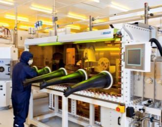
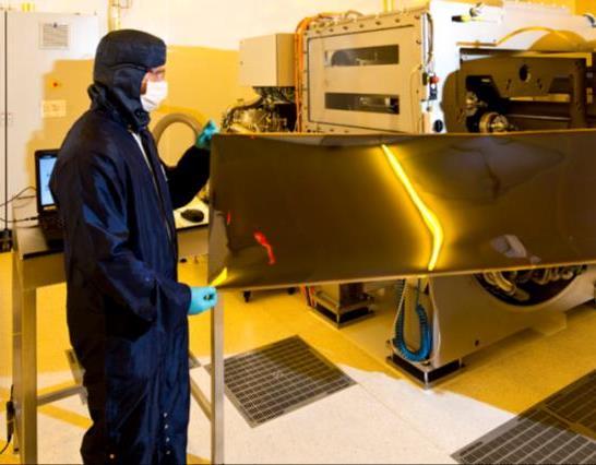
6 Printable Electronics at CPI World class, open-access capability in the scale-up and commercialisation of printable electronic applications 1500m 2 of clean room facilities


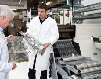
7 Organic Large Area Electronics Optoelectronics Materials Barrier Encapsulation Integrated Smart Systems

 to GEN2")
8 Optoelectronics Extensive capability to support the development and production of Solid State Lighting and PV technologies Product and process scale-up from proof of concept (100mm) to GEN2 (370 x 470mm)


9 Materials Development and prototyping for OTFT Material Studies: flexible substrates, dielectrics, photoresists and organic semiconductors Contract Development of OSC formulations and OTFT


10 Barrier Encapsulation Roll to Roll Atomic Layer Deposition (ALD) Batch Atomic Layer Deposition A range of other sputtering and vacuum coating technologies


11 Integrated Smart Systems Functional items produced by the integration of conventional electronic components with devices prepared by large area printing processes. Printing of antennae, M2M communications devices, and sensors.

12 Applications of Large Area Organic Electronics Photovoltaics and Solid State Lighting Thin film Transistors and Flexible Display Sensors and Biosensors Energy Storage Hybrid Devices Wearable Devices Internet of Things Machine to Machine communication

13 Case Studies

14 Organic Thin Film Transistors CPI is working with UK SMEs for the application of organic semiconductor materials to Organic Thin Film Transistor Arrays. CPI maintains a world class facility for the development and pilot production of OTFTs on flexible polymer substrates

15 PolyPhotonix Established in 2009, PolyPhotonix is a materials science and biophotonic research and development company. Grown from 1 employee to >25


16 Cohda Design Cohda s Crypsis Lighting offers wireless ultra-bright LEDs that can be repositioned and dimmed within a transparent glass panel using an external magnetic control puck
17 PragmatIC PragmatIC has unique patented technologies to manufacture flexible integrated circuits on ultra-thin plastic delivering low-cost intelligent electronics
18 PragmatIC thin, flexible, transparent, robust, disposable


19 Sapient Sensors The creation of a low cost, single use diagnostic sensor for use in a handheld device providing Point of Contact customised screening for a range of diseases, initially Bovine Tuberculosis, without requirement for pathology laboratory support.


20 Integrated Smart Systems (Hybrid approach) Functional items produced by the integration of electronic components with circuits prepared by traditional printing processes +


21 Integrated Smart Systems at CPI Combination of traditional print and conventional electronics equipment Print industry recognised equipment Non cleanroom location Nilpeter roll to roll printing press Litho UV / Conventional Screen UV and WB Flexo UV / Solvent / WB Gravure Solvent Heraeus NIR drying Europlacer Lineo Pick and Place Electronic component attach Conductive adhesive dispense
22 Hybrid approach Printed Power Printed battery (Enfucell, Blue Spark) Thin film solar cell NFC power source Display Electrochromic (Ynvisible) E ink displays OLED (CPI) Memory/Logic Printed logic (PragmatIC Printing) Printed memory (Thin Film ) Printed transistors Circuit Printed conductive tracks Printed dielectrics Light OLED (CPI) Electroluminescence Sensing Mechanical - Electrochemical - Bio-sensor Conventional Power Conventional batteries Mains NFC power source Display LCD Electronic Components Si Chip Resistors Transistors Circuit PCB Flexible PCB Light LED Edge lit LED Sensing Silicon MEMS
23 PROJECT SCOPE Supply Chain Opportunity for Printed Electronics applying highly automated integration techniques to eventually meet target costs of <1c/NFC tag. bringing the technology supply-chain together with integrators, convertors and end users. And providing the means for end-users to find, qualify and engage partners to develop their product concepts, to prove feasibility and market appeal for products. enabling pilot-scale commercial deployment and subsequent transfer to volume production. providing a sustainable platform to develop increasingly advanced functionality for NFC enabled products, whilst also delivering recyclability of products not possible with conventional electronics.

24 PROJECT SCOPE Supply Chain Opportunity for Printed Electronics

25 Technology readiness perspective

26 Photonic Sintering
27 Roll to Roll High Speed Integration SCOPE Project will invest in new technology in 2016
28 Thank you... For more information visit
29
Printable Electronics
 Printable Electronics Printable Electronics The Centre for Process Innovation From innovation to commercialisation The Centre for Process Innovation From innovation to commercialisation The High Value
The Future for Printed Electronics
 The Future for Printed Electronics Jon Helliwell National Centre for Printable Electronics 24 October, 2013 Copyright CPI 2013. All rights reserved What is Printed Electronics? Organic and printed electronics
The Centre for Process Innovation
 The Centre for Process Innovation The Centre for Process Innovation From innovation to commercialisation The future inspired... The High Value Manufacturing Catapult is a partnership between industry and
National Centre for Flexible Electronics
 National Centre for Flexible Electronics Tripartite Partnership Government FlexE Centre - A platform for a meaningful interaction between industry and academia. An interdisciplinary team that advances
Innovation Integrator
 Innovation Integrator Innovation Integrator The Centre for Process Innovation Making successful innovation happen The Centre for Process Innovation From innovation to commercialisation The High Value Manufacturing
The go-to place for advanced manufacturing technologies in the UK
 The go-to place for advanced manufacturing technologies in the UK Introduction Bob Gilbert Chair HVM Catapult The High Value Manufacturing Catapult works with government, academia and industry partners
Printing Beyond Color. Printed Smart Objects on Advanced Paper Substrates. Reinhard R. Baumann
 Printing Beyond Color Printed Smart Objects on Advanced Paper Substrates June 17, 2009 member of Reinhard R. Baumann member of Chemnitz University of Technology Institute for Print and Media Technology
EU Research project proposals (call for Finnish companies)
") EU Research project proposals (call for Finnish companies) 11th EEMELI Workshop 29 th August 2012 Jukka Hast Research Professor VTT Technical Research Centre of Finland 04/10/2012 2 General ICT theme work
EU Research project proposals (call for Finnish companies) 11th EEMELI Workshop 29 th August 2012 Jukka Hast Research Professor VTT Technical Research Centre of Finland 04/10/2012 2 General ICT theme work
ORGANIC ELECTRONICS: PHOTOLITHOGRAPHY OR PRINTING. Giles Lloyd Flex Europe Conference, 25th October 2016
 ORGANIC ELECTRONICS: PHOTOLITHOGRAPHY OR PRINTING Giles Lloyd Flex Europe Conference, 25th October 2016 Organic Electronics: Photoligthography or Printing? Lithography Printing Enabling flexible TFT sheet-fed
Analysis of Wet Coating Thickness Effect on Transparent Conductive Electrode Performance using Silver Nanowire
 Analysis of Wet Coating Thickness Effect on Transparent Conductive Electrode Performance using Silver Nanowire 2017. 04. 25 Seung-Hyun Lee, PhD Senior Researcher Dept. Printed Electronics Korea Institute
Printed and Hybrid Integration
 Printed and Hybrid Integration Neil Chilton PhD Technical Director, Printed Electronics Limited, UK Neil.Chilton@PrintedElectronics.com Printed Electronics Limited (PEL) General Overview PEL was founded
 Organic and flexible Electronics in Saxony www.invest-in-saxony.com WElCOME Organic electronics are based on the discovery that specific organic materials possess semiconducting properties. Functional
Flexible Electronics: Revolutionary Products and Career Opportunities for Creative Engineers
 Flexible Electronics: Revolutionary Products and Career Opportunities for Creative Engineers TAPPI - PIMA Student Summit 2011 Michael Ciesinski President January 15, 2011 Microelectronics changed the world
Printed Electronics - Quo Vadis? What is Printed Electronics et Quo Vadis?
 Printed Electronics - Quo Vadis? Emil J.W. List Institute of Solid State Physics Graz University of Technology NanoTecCenter Weiz Forschungsgesellschaft mbh Agenda Introduction Motivation What is Printed
PILOT LINE FOR LARGE-AREA PRINTING OF ELECTRONIC AND PHOTONIC DEVICES. Simon Perraud, Ph.D. Vice president for European affairs
 PILOT LINE FOR LARGE-AREA PRINTING OF ELECTRONIC AND PHOTONIC DEVICES Simon Perraud, Ph.D. Vice president for European affairs ABOUT LITEN Liten is the research institute of CEA devoted to clean energy
Horizon 2020 and Photonics
 Brussels, 13 December 2013 Horizon 2020 and Photonics Thomas Skordas Head of the Photonics Unit, DG CONNECT European Commission Thomas.Skordas@ec.europa.eu Horizon 2020 Horizon 2020 Budget: 78.6 B (in
shaping global nanofuture ULTRA-PRECISE PRINTING OF NANOMATERIALS
 shaping global nanofuture ULTRA-PRECISE PRINTING OF NANOMATERIALS WHO ARE WE? XTPL S.A. is a company operating in the nanotechnology segment. The interdisciplinary team of XTPL develops on a global scale
Large Area, Flexible Electronics TWG. Chair: Dan Gamota, Jabil
 Large Area, Flexible Electronics TWG Chair: Dan Gamota, Jabil Large Area Flexible Electronics Roadmap History 09/2005 inemi Stakeholders identify Flexible Electronics as Future Growth Market and authorize
EU's contribution to research and innovation in Electronics
 EU's contribution to research and innovation in Electronics Henri.RAJBENBACH@ec.europa.eu Nikolaos.KYRLOGLOU@ec.europa.eu European Commission DG CONNECT (not legally binding presentation) SEMICON Europa-Flex
High Value Manufacturing Catapult
 High Value Manufacturing Catapult Dr Daniel Thompson Senior Technology Officer @ National Composites Centre HVM Catapult Presentation 11 February 2016 UK Manufacturing the Facts The global manufacturing
Здра вствуйте, това рищи!
 Manufacturing of Smart Objects by Printing Technologies Здра вствуйте, това рищи! Moscow / RUS, June 05, 2013 Reinhard R. Baumann Chemnitz University of Technology Chair of Digital Printing Fraunhofer
Heterogeneous integration of autonomous smart films based on electrochromic transistors
 of autonomous smart films NEWSLETTER #5 www.smartwww.smart-ec.eu Objectives SMART-EC has finalized last August 2014; it aimed at the development of self-powered electrochromic (EC) display device with
Low Temperature Integration of Thin Films and Devices for Flexible and Stretchable Electronics
 Low Temperature Integration of Thin Films and Devices for Flexible and Stretchable Electronics Pooran Joshi, Stephen Killough, and Teja Kuruganti Oak Ridge National Laboratory FIIW 2015 Displays and PV
Advancing Consumer Packaging Through Printable Electronics
 IPST Executive Conference, Atlanta, GA March 9-10, 2011 Advancing Consumer Packaging Through Printable Electronics Bernard Kippelen Professor, School of Electrical and Computer Engineering Director, Center
Printed Electronics. Applications
 Printed Electronics Research Through University-Industry Partnerships Outline Background on Printed Electronics (PE) Corporate Partnerships Raytheon UMass Lowell Research Institute (RURI) Printed Electronics
Flexible Hybrid Electronics Fabricated with High-Performance COTS ICs using RTI CircuitFilm TM Technology
 Flexible Hybrid Electronics Fabricated with High-Performance COTS ICs using RTI CircuitFilm TM Technology Scott Goodwin 1, Erik Vick 2 and Dorota Temple 2 1 Micross Advanced Interconnect Technology Micross
Ubiquitous Displays and Sensors Activating Surfaces with Flexible Electronics. Dean Baker, Director FlexEnable. APAC Innovation Summit 2016, Hong Kong
 Ubiquitous Displays and Sensors Activating Surfaces with Flexible Electronics Dean Baker, Director FlexEnable, Hong Kong Activating surfaces with flexible displays and sensors Flexible Plastic Displays
PRINTED ELECTRONICS 3
 PRINTED ELECTRONICS 3 4 INKTEC PRINTED ELECTRONICS 5 6 INKTEC PRINTED ELECTRONICS 7 InkTec Leads New Paradigm in Printed Electronic Materials Applications OTFT, Memory Cell, Display, RFID and so on Product
Hermetic Packaging Solutions using Borosilicate Glass Thin Films. Lithoglas Hermetic Packaging Solutions using Borosilicate Glass Thin Films
 Hermetic Packaging Solutions using Borosilicate Glass Thin Films 1 Company Profile Company founded in 2006 ISO 9001:2008 qualified since 2011 Headquarters and Production in Dresden, Germany Production
Funding New Innovations
 Funding New Innovations Dr Belinda Clarke Lead Technologist, Biosciences (Synthetic Biology) email: belinda.clarke@tsb.gov.uk twitter: @Belinda_Clarke What is the problem we are addressing? Business investment
Processes for Flexible Electronic Systems
 Processes for Flexible Electronic Systems Michael Feil Fraunhofer Institut feil@izm-m.fraunhofer.de Outline Introduction Single sheet versus reel-to-reel (R2R) Substrate materials R2R printing processes
GLOBAL MARKETS, TECHNOLOGIES AND MATERIALS FOR THIN AND ULTRATHIN FILMS
 GLOBAL MARKETS, TECHNOLOGIES AND MATERIALS FOR THIN AND ULTRATHIN FILMS SMC057C August Margareth Gagliardi Project Analyst ISBN: 1-62296-338-5 BCC Research 49 Walnut Park, Building 2 Wellesley, MA 02481
Printable, Novel CNT Inks with V2V Technology
 Printable, Novel CNT Inks with V2V Technology William J. Hurley, Jr., PhD Chasm Technologies, Inc. Canton, MA June 23, 2010 New England Nanomanufacturing Summit 1 Outline CHASM Overview Alliance with SWeNT
Accelerating Growth and Cost Reduction in the PV Industry
 Accelerating Growth and Cost Reduction in the PV Industry PV Technology Roadmaps and Industry Standards An Association s Approach Bettina Weiss / SEMI PV Group July 29, 2009 SEMI : The Global Association
THIS IS INNOVATION Compound Semiconductors
 THIS IS INNOVATION Compound Semiconductors E N A B L I N G This is a quiet industrial revolution, nudging forward the capabilities of the electronics which hide inside nearly every modern day device and
Open Innovation to Manage Risks in Technology The Business of Breakthroughs
 Open Innovation to Manage Risks in Technology The Business of Breakthroughs Janos Veres, Program Manager 2016 PARC, All rights reserved. PARC Legacy: A Storied History of Inventing the Future 1970 1973
ICT 29 : Development of novel materials and systems for OLED lighting
 ICT 29 : Development of novel materials and systems for OLED lighting Martyn Chamberlain Photonics Unit DG CONNECT - European Commission 14 February 2014 Photonics PPP: Overview of Calls 2014-15 (28 M
For personal use only
 Pooled Development Fund funding Australian SME owned projects in technology and resources. Specialty focus on backing projects with large scale upside potential. Maintain significant control over direction
Henkel solutions enabling printed electronics. Dr. Crystal Yang
 Henkel solutions enabling printed electronics Dr. Crystal Yang Agenda 1. Introduction Henkel 2. Trends in Printed Electronics 3. Novel materials enabling Printed Electronics New high speed printable silver
Printed Electronics Product Types & Markets. Vince Cahill, VCE Solutions
 Printed Electronics Product Types & Markets Vince Cahill, VCE Solutions Printed Electronic Product Types Printed circuits boards Printed logic / memory Printed batteries Membrane switches Photovoltaics
EMERGING INKJET PRINTING TECHNOLOGIES, APPLICATIONS AND GLOBAL MARKETS
 EMERGING INKJET PRINTING TECHNOLOGIES, APPLICATIONS AND GLOBAL MARKETS AVM091B November 2014 Andrew McWilliams Project Analyst ISBN: 1-56965-999-0 BCC Research 49 Walnut Park, Building 2 Wellesley, MA
DuPont Reflections on Photovoltaics
 DuPont Reflections on Photovoltaics Steven C. Freilich Technology Director E. I. du Pont de Nemours and Co. CTO Electronics and Communication April 23, 2009 The Vision of DuPont 2 To be the world s most
ICT Micro- and nanoelectronics technologies
 EPoSS Proposers' Day, 2 Feb 2017, Brussels ICT 31-2017 Micro- and nanoelectronics technologies Eric Fribourg-Blanc, Henri Rajbenbach, Andreas Lymberis European Commission DG CONNECT (Communications Networks,
UVISEL. Spectroscopic Phase Modulated Ellipsometer. The Ideal Tool for Thin Film and Material Characterization
 UVISEL Spectroscopic Phase Modulated Ellipsometer The Ideal Tool for Thin Film and Material Characterization High Precision Research Spectroscopic Ellipsometer The UVISEL ellipsometer offers the best combination
For personal use only
 For personal use only 7 JUNE 2017 ASX MEDIA RELEASE Nanocube Memory Ink Development Progress Strategic Elements Ltd (ASX : SOR) is pleased to provide an update on the Nanocube Memory ink invented by the
OLAE in Horizon 2020 LEIT ICT WP DG CONNECT - European Commission
 OLAE in Horizon 2020 LEIT ICT WP 2014-15 DG CONNECT - European Commission 11 December 2013 Horizon 2020, Industrial Leadership (LEIT) Priority An Overview of Calls related to OLAE LEIT ICT 3 2014 Advanced
Energy & Space. International Presentations
 Energy & Space International Presentations 2012-2013 Advanced Electronics 3D Printed Circuit Boards 3D Printed Circuit Boards for Solder-Free Printable Electronics 4x4 Vehicles Arduino WiFi Android Controllers
In 1984, a cell phone in the U.S. cost $3,995 and
 In 1984, a cell phone in the U.S. cost $3,995 and weighed 2 pounds. Today s 8GB smartphones cost $199 and weigh as little as 4.6 oz. Technology Commercialization Applied Materials is one of the most important
Workshop on Enabling Technologies in CSF for EU Research and Innovation Funding
 Workshop on Enabling Technologies in CSF for EU Research and Innovation Funding Rapporteur Professor Costas Kiparissides, Department of Chemical Engineering, Aristotle University of Thessaloniki Brussels,
GSM OPTICAL MONITORING FOR HIGH PRECISION THIN FILM DEPOSITION
 OPTICAL MONITORING FOR HIGH PRECISION THIN FILM DEPOSITION OPTICAL MONITORING TECHNOLOGIES ENABLING OUR NEW WORLD! - ACHIEVING MORE DEMANDING THIN FILM SPECIFICATIONS - DRIVING DOWN UNIT COSTS THE GSM1101
WP Topic LEIT ICT 3 Advanced TOLAE technologies
 Brussels, 14 February 2014 Information and Networking Day WP 2014-15 Topic LEIT ICT 3 Advanced TOLAE technologies Philippe Reynaert and Andreas Lymberis Project Officer, Unit A1 and A4, DG CONNECT European
Figure 1 - IMSE (courtesy of TaktoTek)
") Screen Printing the Third Industrial Revolution Since its infancy hundreds of years ago, until widespread adoption in the mid/late 20 th century, screen printing has been used primarily to create media
Screen Printing the Third Industrial Revolution Since its infancy hundreds of years ago, until widespread adoption in the mid/late 20 th century, screen printing has been used primarily to create media
Passive Direct Print Sensors
 Passive Wireless Sensor Technology Workshop June 6-7, 2012 Hyatt Regency, La Jolla, CA Passive Direct Print Sensors Mike Newton mnewton@nscrypt.com nscrypt Inc. Orlando, Florida University of Texas at
Specialization in Microelectronics. Wang Qijie Nanyang Assistant Professor in EEE March 8, 2013
 Specialization in Microelectronics Wang Qijie Nanyang Assistant Professor in EEE qjwang@ntu.edu.sg March 8, 2013 Electronic Engineering Option Microelectronics What is it about? Study of semiconductor
Holst Centre Wireless Autonomous Sensor Technologies & Flexible Electronics
 February 10, 2011 Holst Centre Wireless Autonomous Sensor Technologies & Flexible Electronics Presentation overview -General overview -Research focus < 4 Holst Centre: a solid partner in research Independent,
Feature-level Compensation & Control
 Feature-level Compensation & Control 2 Sensors and Control Nathan Cheung, Kameshwar Poolla, Costas Spanos Workshop 11/19/2003 3 Metrology, Control, and Integration Nathan Cheung, UCB SOI Wafers Multi wavelength
End-of-line Standard Substrates For the Characterization of organic
 FRAUNHOFER INSTITUTe FoR Photonic Microsystems IPMS End-of-line Standard Substrates For the Characterization of organic semiconductor Materials Over the last few years, organic electronics have become
Large area cost-efficient electronics integration. Flexible Substrate Polytronische Systeme
 Large area cost-efficient electronics integration. Flexible Substrate Polytronische Systeme Institut Zuverlässigkeit und Mikrointegration Institutsteil München Karlheinz Bock for Hansastr. 27d, D-80686
Complementary Organic Semiconductor and Metal Integrated Circuits
 Complementary Organic Semiconductor and Metal Integrated Circuits COSMIC will generate an organic CMOS technology platform from design to manufacturing level. COSMIC will produce highly complex lead applications
MID Manufacturing Process.
 3D Aerosol Jet Printing An Emerging MID Manufacturing Process. Dr. Martin Hedges Neotech Services MTP, Nuremberg, Germany info@neotechservices.com Aerosol Jet Printing Aerosol Jet Process Overview Current
Printed Electronics: success stories and future commercial applications
 Printed Electronics: success stories and future commercial applications Dr Guillaume Chansin @gchansin June 2017 Helping you profit from emerging technologies Advantages of printed electronics Mass production
SCREEN PRINTING ELECTRONICS
 I am sure that people who do not have to write for a living think that we scribes sit with ideas bursting out of our fingertips just waiting for the next opportunity to bore the pants off our readership.
CMOS Digital Integrated Circuits Lec 2 Fabrication of MOSFETs
 CMOS Digital Integrated Circuits Lec 2 Fabrication of MOSFETs 1 CMOS Digital Integrated Circuits 3 rd Edition Categories of Materials Materials can be categorized into three main groups regarding their
CHEMISTRY AND PHARMACEUTICALS PATENT ATTORNEYS TRADE MARK ATTORNEYS
 CHEMISTRY AND PHARMACEUTICALS PATENT ATTORNEYS TRADE MARK ATTORNEYS INDEPENDENT THINKING. COLLECTIVE EXCELLENCE. Your intellectual property assets are of great value to you. To help you to secure, protect
Making a Material Difference
 Making a Material Difference Founded as a QinetiQ corporate investment in January 2002 Spun out in 2007 Locations: Rochester, NYS, USA (HQ and Production) Farnborough and Malvern, UK (R&D, Production and
NextFlex: Enabling a Domestic Manufacturing Ecosystem for Flexible Hybrid Electronics (Extended Abstract)
") NextFlex: Enabling a Domestic Manufacturing Ecosystem for Flexible Hybrid Electronics (Extended Abstract) Benjamin J. Leever*, Eric W. Forsythe + *Air Force Research Laboratory, 2179 12th St., B652/R122,
NextFlex: Enabling a Domestic Manufacturing Ecosystem for Flexible Hybrid Electronics (Extended Abstract) Benjamin J. Leever*, Eric W. Forsythe + *Air Force Research Laboratory, 2179 12th St., B652/R122,
Flexible Glass Applications & Process Scaling
 Flexible Glass Applications & Process Scaling Sean Garner, Sue Lewis, Gary Merz, Alex Cuno, Ilia Nikulin October 16, 2017 Outline Flexible Glass Applications Process Scaling Summary 2 Flexible Glass Enables
NTU RECIPIENTS OF NRF S PROOF OF CONCEPT SCHEME GRANTS. 1. A Semantics-Based and Service-Oriented Framework for the Virtualisation of Sensor Networks
 Reg. No. 200604393R FACT SHEET For immediate release Total: 7 pages including this page Singapore, 21 August 2009 NTU RECIPIENTS OF NRF S PROOF OF CONCEPT SCHEME GRANTS 1. A Semantics-Based and Service-Oriented
Potential Induced degradation
 Potential Induced degradation By: Waaree Energies Limited Abstract The PID defect is affecting all the manufacturers around the world. This defect is byproducts of the aggressive competition in the solar
6-7 October Marina Bay Sands Expo & Convention Centre Peony Ballroom [Level 4]
![6-7 October Marina Bay Sands Expo & Convention Centre Peony Ballroom [Level 4]](/thumbs/80/80853998.jpg "6-7 October Marina Bay Sands Expo & Convention Centre Peony Ballroom [Level 4]") camline http://www.camline.com Booth 22 camline s mission is to provide the highest quality software solutions for factory automation and logistics, helping global manufacturers maintain their competitive
camline http://www.camline.com Booth 22 camline s mission is to provide the highest quality software solutions for factory automation and logistics, helping global manufacturers maintain their competitive
Innovative Vacuum Solutions
 100.131.02 Innovative Vacuum Solutions for Flat Panel Display Vacuum Solutions for DRYVAC SYSTEMS THE LEYBOLD STANDARD for Flat Panel Display With our DRYVAC SYSTEM platform we offer innovative solutions
Compound Semiconductor Center
 Compound Semiconductor Center Compound Semiconductor Centre Building a Technology Cluster in South Wales Dr Wyn Meredith Status October 2015 Formal JV: 50:50 Cardiff University: IQE Academia Public Sector
DOE Project: Resist Characterization
 DOE Project: Resist Characterization GOAL To achieve high resolution and adequate throughput, a photoresist must possess relatively high contrast and sensitivity to exposing radiation. The objective of
Compound Semiconductor Applica2ons Catapult Technology Scotland, 4 th May 2016
 Compound Semiconductor Applica2ons Catapult Technology Scotland, 4 th May 2016 Andy Sellars, MBA, PhD, MSc Lead Technologist, Manufacturing & Materials andy.sellars@innovateuk.gov.uk @andy_g_sellars Delivery
Lightweight, High-Efficiency Solar Cells. Aarohi Vijh. Company
 Lightweight, High-Efficiency Solar Cells arohi Vijh History lta Devices Founded World renowned founders CalTech Professor Harry twater Berkeley Professor Eli Yablonovitch lta sets records Single Junction
Micro-PackS, Technology Platform. Security Characterization Lab Opening
 September, 30 th 2008 Micro-PackS, Technology Platform Security Characterization Lab Opening Members : Micro-PackS in SCS cluster From Silicium to innovative & commucating device R&D structure, gathering
Paper Electronics Paper as Substrate for Printed Electronics and Sensors. Martti Toivakka Åbo Akademi University
 Paper Electronics Paper as Substrate for Printed Electronics and Sensors Martti Toivakka Åbo Akademi University Printed Electronics has Created Hype (and Unreasonable Expectations ) Paper Electronics =
1.1 PHILOSOPHY OF MICRO/NANOFABRICATION
 CHAPTER Introduction 1 C H A P T E R C O N T E N T S 1.1 Philosophy of Micro/Nanofabrication... 1 1.2 The Industry Science Dualism... 5 1.3 Industrial Applications... 8 1.4 Purpose and Organization of
Radial Coupling Method for Orthogonal Concentration within Planar Micro-Optic Solar Collectors
 Radial Coupling Method for Orthogonal Concentration within Planar Micro-Optic Solar Collectors Jason H. Karp, Eric J. Tremblay and Joseph E. Ford Photonics Systems Integration Lab University of California
From vision to growth: Role of research in building world-class excellence in future added value electronics
 From vision to growth: Role of research in building world-class excellence in future added value electronics Antti Vasara, CEO VTT Technical Research Centre of Finland Ltd Contents 1. VTT in short 2. Our
Plastic Electronics Market Development. by Mr. Ed van den Kieboom Executive Board Member Plastic Electronics Foundation
 Plastic Electronics Market Development by Mr. Ed van den Kieboom Executive Board Member Plastic Electronics Foundation Plastic Electronics Foundation Established April 2005 Private non profit organization
M J.A. Woollam Co., Inc. Ellipsometry Solutions
 M-2000 J.A. Woollam Co., Inc. Ellipsometry Solutions Speed Discover the Difference Focused M-2000 The M-2000 line of spectroscopic ellipsometers is engineered to meet the diverse demands of thin film characterization.
Additive & Inkjet Printing Technologies & Applications
 Additive & Inkjet Printing Technologies & Applications Debbie Thorp, Business Development Director Global Inkjet Systems Ltd Silverstone Park - October 2018 GIS Products DFE Atlas User Interface Machine
New Horizons. A new paradigm. of collaborative research
 New Horizons A new paradigm of collaborative research One of the immediate and complex challenges facing industry, business and government in Australia today is a need to increase exports, foreign investment
PRINTED ELECTRONICS TECHNOLOGIES
 PRINTED ELECTRONICS TECHNOLOGIES YEARS OF R&D DRIVEN BY CONTINUOUS INNOVATION HAVE POSITIONNED GGI SOLUTIONS AS A LEADER IN PRINTED ELECTRONICS TECHNOLOGIES 2 As a level 1 member of the Printable Electronics
2020 at the Horizon. Upcoming calls in Electronics. "Competitive Electronics Industry" "Digital Industry" "CONNECT"
 2020 at the Horizon Upcoming calls in Electronics Andreas Lymberis-Henri Rajbenbach Unit A3: Directorate: Directorate General: "Competitive Electronics Industry" "Digital Industry" "CONNECT" Electronic
Projects and Partners Working with Chalcogenide Advanced Manufacturing Partnership (ChAMP)
") Projects and Partners Working with Chalcogenide Advanced Manufacturing Partnership (ChAMP) Dr John Lincoln Industrial Liaison Officer j.lincoln@soton.ac.uk March 2015 ChAMP Aims Establish world leading
Projects and Partners Working with Chalcogenide Advanced Manufacturing Partnership (ChAMP) Dr John Lincoln Industrial Liaison Officer j.lincoln@soton.ac.uk March 2015 ChAMP Aims Establish world leading
Nanotechnology, the infrastructure, and IBM s research projects
 Nanotechnology, the infrastructure, and IBM s research projects Dr. Paul Seidler Coordinator Nanotechnology Center, IBM Research - Zurich Nanotechnology is the understanding and control of matter at dimensions
Issue 2 March Electroluminescent Materials
 Electroluminescent Materials Issue 2 March 2017 Electroluminescent Materials Overview. Product Range. GEM s products are based on a unique curing process that results in the low temperature formation of
MICROFLEX Project: MEMS on New Emerging Smart Textiles/Flexibles
 MICROFLEX Project: MEMS on New Emerging Smart Textiles/Flexibles S Beeby, M J Tudor, R Torah, K Yang, Y Wei Dr Steve Beeby ESD Research Group Smart Fabrics 2011 5 th April 2011 Overview Introduce the MicroFlex
Application Bulletin 240
 Application Bulletin 240 Design Consideration CUSTOM CAPABILITIES Standard PC board fabrication flexibility allows for various component orientations, mounting features, and interconnect schemes. The starting
Our Aspirations Ahead
 Our Aspirations Ahead ~ Pursuing Smart Innovation ~ 1 Introduction For the past decade, under our corporate philosophy Creating a New Communication Culture, and the vision MAGIC, NTT DOCOMO Group has been
Existing and Emerging Opportunities in Printed Electronics For Printers
 Existing and Emerging Opportunities in Printed Electronics For Printers Don Banfield Conductive Compounds, Inc. Hudson, New Hampshire, USA www.conductivecompounds.com Presentation Outline Summary of some
Outstanding performance starts with the selection of your masterbatch partner. Your expert in masterbatches and compounds. sukano.
 Driven by expertise Outstanding performance starts with the selection of your masterbatch partner Your expert in masterbatches and compounds Sukano is a world leader in the development and production of
Put your best ideas forward.
 Improve the way people view your brand. High-performance optical polymers and films for the electronics market Put your best ideas forward. The world is increasingly connected by technology that uses electronic
Surrey Knowledge Transfer Account
 Surrey Knowledge Transfer Account Innovation Powered. Innovation Powered Innovation is vital if the UK is to remain competitive on the world stage. The University of Surrey has a track record of successful
Innovation Partnering
 Innovation Partnering Proof-of-Concept Services Advancing Research and Commercial Possibilities The California Institute for Telecommunications and Information Technology Irvine Prof. Mark Bachman Prof.
For Immediate Release. For More PR Information, Contact: Carlo Chatman, Power PR P (310) F (310)
 F (310)") For Immediate Release For More PR Information, Contact: Carlo Chatman, Power PR P (310) 787-1940 F (310) 787-1970 E-mail: press@powerpr.com Miniaturized Wireless Medical Wearables Tiny RF chip antennas
For Immediate Release For More PR Information, Contact: Carlo Chatman, Power PR P (310) 787-1940 F (310) 787-1970 E-mail: press@powerpr.com Miniaturized Wireless Medical Wearables Tiny RF chip antennas
Flexible Substrates and SCB-Technology
 Flexible Substrates and SCB-Technology Substrate Technology As requirements are increasing, so are electronic systems becoming smaller and smaller and more complex. In its role as innovative forerunner
HipoCIGS: enamelled steel as substrate for thin film solar cells
 HipoCIGS: enamelled steel as substrate for thin film solar cells Lecturer D. Jacobs*, Author S. Efimenko, Co-author C. Schlegel *:PRINCE Belgium bvba, Pathoekeweg 116, 8000 Brugge, Belgium, djacobs@princecorp.com