Passive Direct Print Sensors
|
|
|
- Alisha Dorsey
- 5 years ago
- Views:
Transcription

1 Passive Wireless Sensor Technology Workshop June 6-7, 2012 Hyatt Regency, La Jolla, CA Passive Direct Print Sensors Mike Newton nscrypt Inc. Orlando, Florida University of Texas at El Paso University of South Florida
2 Digital Fabrication Technology Printed Electronics 3D Additive manufacturing Convergent Technologies Direct Print Additive Manufacturing * The third industrial revolution The digitization of manufacturing will transform the way goods are made and change the politics of jobs too


3 Direct Print Equipment Printing heads/pump Smartpump TM Positive displacement pump Mixer Sprayer Vision Processing camera Automatic guidance/alignment Post process inspection Others Laser machining/curing Rotary as 4 th axis Heat option for stage and pump Pic and Place UV Cure
4 Direct Print Equipment Conventional Dispensing: Pros Direct material deposition Low cost & easy setup Relatively flexible on Material choice Cons Slow Lack of accuracy Limited consistency Limited feature size Micro-Dispensing/direct printing: High speed As fast as 500mm/sec. Wide range of material choice: viscosity from 1cps to >1 million cps. Type of materials can be processed but not limited to conductive, dielectric, adhesive, solder, epoxy, encapsulate, hot melt, silicone oil, biological chemicals, live cells and etc. Capability of high resolution and accuracy Pico-liter level column control Line as small as 20um, dot as small as 75um.


5 Direct Print Equipment Standard SmartPump TM


6 Direct Print Process - It is possible to print fine lines with exceptional start/stop. - If there surface is not completely flat, it is possible to accommodate that without scanning. - It is possible to utilize a layering approach to build structures if the material is viscous. - There are number of issues that must be resolved, but one of the biggest issues.. Software.


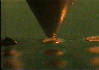
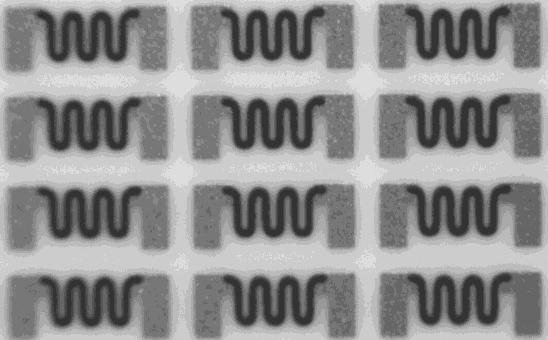
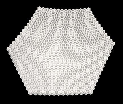
7 Direct Printed Gridline Representative SEM images of direct printed gridline* *X. Chen, K. Church, H. Yang, 35th IEEE PVSC (2010).

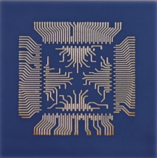
8 Directly Printed Electronics sensors resistors 3D scaffold solar cell solder and via micro lens breakout pattern working device


9 A Hierarchy of System Packaging $ Bare Die Package of Packages $ Packaged Die $ $ Packaged Circuit Board Sub Assembly $ Packaged Chassis Assembly $ Packaged Rack Assembly


10 Volumetric Inefficient Packaging Size, Weight and Power Hardware/Fasteners/Connectors drive SWaP in the wrong direction


11 Shifting the Packaging Paradigm


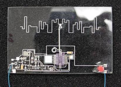
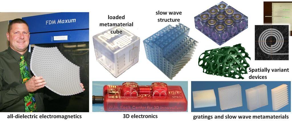
12 Directly Printed Functional Structures UAV wing with strain sensor Magnetometer Vibration sensor Electronic circuits Monolithic dice Loaded metamaterial cube


 Print")
13 Direct Print Material Selection very wide Ceramic loaded UV curable mixture Metal loaded silicone Breakout patterns from 25 micron wide lines to hundreds of microns wide. Robotic and dispense precision for bare die (when performance is needed) Print what you can.place what you can t.


14 Material and Test Structure Mix UV curable material with ceramic powder 25% DSM Somos by volume Viscosity ~ C Density C 75% Ceramic Powder by volume Melting Point 2050 C Specific Gravity Specific Surface Area 13.5 m2/g Avg Particle Size.17 µm Standard structure for mechanical testing Loaded and mixed material can be stored and used in a syringe. This allows for easier storage and reduced waste. From the syringe it is printed directly onto a substrate or a structure.


15 Direct Print Additive Manufacturing DPAM DPAM is being used to build 3D structures: Dog Bones A standard size is being utilized to build a data base for a variety of materials to include loaded and unloaded UV curable polymers. The loading can be carbon micro or nano strings, ceramic, titanium, iron particles that can be micro or nano in size. Diverse loadings create a unique ability to vary and control the material properties and the concept of multiple pens enables heterogeneous properties in a homogeneous build.


16 Print and Post Cure Process DPAM was used to print dog bones and after each layer was printed, UV curing was done. Cure Speed Spot Size Max Irradiance Cure Height 5 mm/s 3 mm 9500 mw/cm2 10 mm Pen Tip 125/175 µm Print Speed 3 mm/s Dispense Gap 100 µm Number of Layers 7 Fill Pitch 100 µm


17 RF microstrip Line Comparison 50 mm microstrip on polymer -3dB at 9.9 GHz Diverse substrates Diverse printable materials Diverse post process parameters DC is easy to get to perform RF is challenging Important to open range of materials to include dielectrics, metals, piezoelectric and more. 50 mm microstrip on LCP -3dB at 14.1 GHz


18 Fabrication PCB Design The data are matched for the PCB design Deviation of 40 MHz between predicted and simulated results with the SLA design. The SLA bandwidth has increased by a factor of 1.8 SLA Design PCB Design SLA Design 18
19 Results S 11 (db) S11 (db) Simulated Measured Frequency (GHz) PCB Design Measured Simulated The data are matched for the PCB design Frequency (GHz) SLA Design Deviation of 40 MHz between predicted and simulated results with the SLA design. The SLA bandwidth has increased by a factor of


20 Direct Print 3D Metamaterials Printed Electromagnetics


21 Direct Print 3D All-Dielectric Antennas Monolithic More options for integration Low observable applications High power capable Extremely low loss Photon detection and collection An option for processes where multimaterials is still difficult. All-dielectric patch antennas

.")
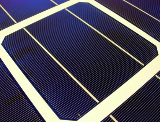
22 Parallel Printing for Solar Industry To meet the solar industry throughput requirement, parallel printing by scaling up the number of nozzles is critical. TM First PV product unit=> Smart Pump PV24 3 Passes at about 300 mm/s => 72 lines 1200 wafer per hour process Performance of these printed cells demonstrate consistently a higher efficiency in performance (0.5% overall improvement). It also demonstrates a reduction in silver use (20%). So what would keep this from dominating front metallization? Speed!!!!!
23 Parallel Printing and Scale-up To meet the manufacturing industry throughput requirement, parallel printing by scaling up the number of nozzles is critical. A new pump that has significant size reduction for this application has been designed

24 Parallel Printing and Scale-up A working multi-nozzle prototype printing head has been assembled and tested. This can be a single material feed or a multi-material feed. multi-nozzle printing head prototype (12 nozzles)


25 Next Generation Ink-Jet Printer will be a Paste Place Printer Gen I => 12 nozzles: either on or off Gen 2 => 12 nozzles: independent control Gen 3 => 24 nozzles: independent, now Gen 4 => 400+ nozzles: Future

26 The Future of Direct Printing
27 Conclusion Printed Electronics will meld with 3D Printing A new 3D printing technique has potential to enhance AM (DPAM) RF 3D has great potential.large obstacle is performance DPAM potential will have obstacles.large obstacle is software To move from Rapid Prototyping to true Rapid Manufacturing..SPEED
28 Passive Wireless Sensor Technology Workshop June 6-7, 2012 Hyatt Regency, La Jolla, CA Passive Direct Print Sensors Mike Newton nscrypt Inc. Orlando, Florida University of Texas at El Paso University of South Florida
3D Printed Electronics for Printed Circuit Structures
 As originally published in the IPC APEX EXPO Proceedings. 3D Printed Electronics for Printed Circuit Structures Samuel LeBlanc, Paul Deffenbaugh, Jacob Denkins, Kenneth Church nscrypt, Inc. Orlando, Florida
3D Printed Electronics for Printed Circuit Structures
 3D Printed Electronics for Printed Circuit Structures Samuel LeBlanc, Paul Deffenbaugh, Jacob Denkins, Kenneth Church nscrypt, Inc. Orlando, Florida Abstract Printed electronics is a familiar term that
Paul Deffenbaugh, Ph.D Senior Scientist nscrypt, Inc. Direct Digital Manufacturing: 3D Printed Electronics Enables Printed Circuit Structures
 Paul Deffenbaugh, Ph.D Senior Scientist nscrypt, Inc. Direct Digital Manufacturing: 3D Printed Electronics Enables Printed Circuit Structures sme.org/smartmfgseries Direct Digital Manufacturing: 3D Printed
Direct-Write Printing of Meshed Patch Antenna on Textile
 Direct-Write Printing of Meshed Patch Antenna on Textile 1 Hasan Shahariar, PhD Candidate 2 Raj Bhakta, PhD Student 3 Dr. Jesse Jur, PI Fiber & Polymer Science, Electrical Engineering Department of Textile
Figure 7 Dynamic range expansion of Shack- Hartmann sensor using a spatial-light modulator
 Figure 4 Advantage of having smaller focal spot on CCD with super-fine pixels: Larger focal point compromises the sensitivity, spatial resolution, and accuracy. Figure 1 Typical microlens array for Shack-Hartmann
Printed and Hybrid Integration
 Printed and Hybrid Integration Neil Chilton PhD Technical Director, Printed Electronics Limited, UK Neil.Chilton@PrintedElectronics.com Printed Electronics Limited (PEL) General Overview PEL was founded
imaps New England 43rd Symposium & Expo May 03, 2016
 Digital Manufacturing and Performance Testing for Application Specific Electronic Packaging (ASEP) imaps New England 43rd Symposium & Expo May 03, 2016 Introduction Why do material choices and tight controls
Visual Imaging in the Electronic Age
 Visual Imaging in the Electronic Age ART 2107, ARCH 3702, CS 1620, ENGRI 1620 3D Printing November 6, 2014 Prof. Donald P. Greenberg dpg5@cornell.edu Types of 3D Printers Selective deposition printers
Processes for Flexible Electronic Systems
 Processes for Flexible Electronic Systems Michael Feil Fraunhofer Institut feil@izm-m.fraunhofer.de Outline Introduction Single sheet versus reel-to-reel (R2R) Substrate materials R2R printing processes
B. Flip-Chip Technology
 B. Flip-Chip Technology B1. Level 1. Introduction to Flip-Chip techniques B1.1 Why flip-chip? In the development of packaging of electronics the aim is to lower cost, increase the packaging density, improve
Fully 3D Printed 2.4 GHz Bluetooth/Wi-Fi Antenna
 Fully 3D Printed 2.4 GHz Bluetooth/Wi-Fi Antenna Paul Deffenbaugh, Kenneth Church The University of Texas El Paso 500 W. University Ave El Paso, TX 79968, US Ph.: 407-275-4720 Email: pdeffenbaugh@miners.utep.edu
Effect of Corona Treatment on Spreading Behavior of UV Ink over Inkjet Printed Silver Nano-Particle Layer
 Effect of Corona Treatment on Spreading Behavior of UV Ink over Inkjet Printed Silver Nano-Particle Layer Khushbeen Department of Printing Technology GJUS&T, Hisar, Haryana, India Email- khushveen12@gmail.com
Fully Printed Conformal Antenna and Sensors on 3D Plastic, Ceramic, and Metallic Substrates. Mike O Reilly
 Fully Printed Conformal Antenna and Sensors on 3D Plastic, Ceramic, and Metallic Substrates Mike O Reilly imaps NE 2016 Antenna and sensor printing via Aerosol Jet Optomec has developed high volume 3D
MID Manufacturing Process.
 3D Aerosol Jet Printing An Emerging MID Manufacturing Process. Dr. Martin Hedges Neotech Services MTP, Nuremberg, Germany info@neotechservices.com Aerosol Jet Printing Aerosol Jet Process Overview Current
Visual Imaging in the Electronic Age
 Visual Imaging in the Electronic Age ART 2107, ARCH 3702, CS 1620, ENGRI 1620 3D Printing October 20, 2015 Prof. Donald P. Greenberg dpg5@cornell.edu Types of 3D Printers Selective deposition printers
3D PRINTED IMPEDANCE ELEMENTS BY MICRO-DISPENSING
 3D PRINTED IMPEDANCE ELEMENTS BY MICRO-DISPENSING UBALDO ROBLES DOMINGUEZ The Department of Electrical and Computer Engineering APPROVED: Raymond C. Rumpf, PhD.,Chair Eric MacDonald, PhD. Peter Kim, PhD.
Electronics Integration in Conformal Substrates Fabricated with Additive Layered Manufacturing Introduction
 Electronics Integration in Conformal Substrates Fabricated with Additive Layered Manufacturing Sylvia Castillo, Dan Muse, Frank Medina, Eric MacDonald and Ryan Wicker The University of Texas at El Paso,
Precise Solder Dispensing In High-Throughput Microdevice Packaging Applications
 Precise Solder Dispensing In High-Throughput Microdevice Packaging Applications A high-precision, highthroughput solder paste dispensing process fills the gap between novel packaging design, traditional
Dispenser printed proximity sensor on fabric for creative smart fabric applications
 Dispenser printed proximity sensor on fabric for creative smart fabric applications Yang Wei, Russel Torah, Yi Li and John Tudor University of Southampton, Southampton, United Kingdom, SO17 3BJ Tel: +44(0)23
AEROSOL JET PRINTING OF CONDUCTIVE EPOXY FOR 3D PACKAGING
 AEROSOL JET PRINTING OF CONDUCTIVE EPOXY FOR 3D PACKAGING Michael J. Renn, Ph.D., and Kurt K. Christenson, Ph.D. Optomec, Inc. St. Paul, MN, USA mrenn@optomec.com and kchristenson@optomec.com Donald Giroux
Midaz Micro-Slab DPSS Lasers:
 Midaz Micro-Slab DPSS Lasers: Higher power & pulse rate for higher speed micromachining Professor Mike Damzen Midaz Laser Ltd 4 June 2008 AILU Meeting Industrial opportunities in laser micro and nano processing
Aerosol Jet technology opportunities
 Aerosol Jet technology opportunities Jiří Navrátil 1. Introduction history and formation 2. Aerosol Jet system 2.1 System components 2.2 Inks and substrates 3. Application of Aerosol Jet technology 4.
Dicing Through Hard and Brittle Materials in the Micro Electronic Industry By Gideon Levinson, Dicing Tools Product Manager
 Dicing Through Hard and Brittle Materials in the Micro Electronic Industry By Gideon Levinson, Dicing Tools Product Manager A high percentage of micro electronics dicing applications require dicing completely
Manufacture and Performance of a Z-interconnect HDI Circuit Card Abstract Introduction
 Manufacture and Performance of a Z-interconnect HDI Circuit Card Michael Rowlands, Rabindra Das, John Lauffer, Voya Markovich EI (Endicott Interconnect Technologies) 1093 Clark Street, Endicott, NY 13760
Energy & Space. International Presentations
 Energy & Space International Presentations 2012-2013 Advanced Electronics 3D Printed Circuit Boards 3D Printed Circuit Boards for Solder-Free Printable Electronics 4x4 Vehicles Arduino WiFi Android Controllers
Radial Coupling Method for Orthogonal Concentration within Planar Micro-Optic Solar Collectors
 Radial Coupling Method for Orthogonal Concentration within Planar Micro-Optic Solar Collectors Jason H. Karp, Eric J. Tremblay and Joseph E. Ford Photonics Systems Integration Lab University of California
Benchmarking of LTCC Circuits up to 40GHz and Comparison with EM Simulation
 CARTS Europe 28 2-23 October Helsinki, Finland Benchmarking of LTCC Circuits up to 4GHz and Comparison with EM Simulation D.E.J. Humphrey, B.Verner, V. Napijalo TDK Electronics Ireland 322 Lake Drive,
Aerosol Jet Printing of Structured Films. Denis Cormier Rochester Institute of Technology
 Aerosol Jet Printing of Structured Films Denis Cormier Rochester Institute of Technology cormier@mail.rit.edu Metal additive manufacturing of engineered titanium lattice structures Local control over strength,
A Miniaturized Multi-Channel TR Module Design Based on Silicon Substrate
 Progress In Electromagnetics Research Letters, Vol. 74, 117 123, 2018 A Miniaturized Multi-Channel TR Module Design Based on Silicon Substrate Jun Zhou 1, 2, *, Jiapeng Yang 1, Donglei Zhao 1, and Dongsheng
Printed Electronics. Applications
 Printed Electronics Research Through University-Industry Partnerships Outline Background on Printed Electronics (PE) Corporate Partnerships Raytheon UMass Lowell Research Institute (RURI) Printed Electronics
Flexible Hybrid Electronics Fabricated with High-Performance COTS ICs using RTI CircuitFilm TM Technology
 Flexible Hybrid Electronics Fabricated with High-Performance COTS ICs using RTI CircuitFilm TM Technology Scott Goodwin 1, Erik Vick 2 and Dorota Temple 2 1 Micross Advanced Interconnect Technology Micross
Novel Packaging Approaches for Miniature Antennas
 Novel Packaging Approaches for Miniature Antennas Will McKinzie, Greg Mendolia, and John Dutton Etenna Corporation 6100-C Frost Place, Laurel, MD 20707 wmckinzie@etenna.com, gmendolia@etenna.com, and jdutton@etenna.com
Printing Processes and their Potential for RFID Printing
 Printing Processes and their Potential for RFID Printing Anne Blayo and Bernard Pineaux, EFPG 1 - Printing processes - A.Blayo and B. Pineaux - soc -EUSAI - 12th October 2005, Grenoble Outline General
AEROSOL JET PRINTING SYSTEM FOR HIGH SPEED, NON-CONTACT FRONT SIDE METALLIZATION OF SILICON SOLAR CELLS
 AEROSOL JET PRINTING SYSTEM FOR HIGH SPEED, NON-CONTACT FRONT SIDE METALLIZATION OF SILICON SOLAR CELLS Bruce H. King and Stephen M. Barnes Optomec, Inc. 3911 Singer NE, Albuquerque, NM 87109, US Phone
Part 5-1: Lithography
 Part 5-1: Lithography Yao-Joe Yang 1 Pattern Transfer (Patterning) Types of lithography systems: Optical X-ray electron beam writer (non-traditional, no masks) Two-dimensional pattern transfer: limited
EMERGING INKJET PRINTING TECHNOLOGIES, APPLICATIONS AND GLOBAL MARKETS
 EMERGING INKJET PRINTING TECHNOLOGIES, APPLICATIONS AND GLOBAL MARKETS AVM091B November 2014 Andrew McWilliams Project Analyst ISBN: 1-56965-999-0 BCC Research 49 Walnut Park, Building 2 Wellesley, MA
Biorelevant Multi- Material Additive Manufacturing at Nottingham. Ricky Wildman. Faculty of Engineering and School of Pharmacy
 Biorelevant Multi- Material Additive Manufacturing at Nottingham Ricky Wildman Faculty of Engineering and School of Pharmacy Contents 3D Printing at Nottingham: EPSRC Centre for Innovative Manufacturing
Direct Digital Manufacturing of Multi-layer Wideband Ku-band Patch Antennas
 University of South Florida Scholar Commons Graduate Theses and Dissertations Graduate School November 2017 Direct Digital Manufacturing of Multi-layer Wideband Ku-band Patch Antennas Merve Kacar University
Printing versus coating technology Which way Printed Electronics with solution coating will go?
 Printing versus coating technology Which way Printed Electronics with solution coating will go? Frank Schäfer, Andrea Glawe, Dr. Daniel Eggerath, KROENERT GmbH& Co KG, Schuetzenstrasse 105, 22761 Hamburg
Just where it s needed
 Seite/Page: 1 Just where it s needed Continuing miniaturisation of many products requires a method of dispensing very small amounts of liquids Inkjet technology is capable of applying adhesives and many
Low Temperature Integration of Thin Films and Devices for Flexible and Stretchable Electronics
 Low Temperature Integration of Thin Films and Devices for Flexible and Stretchable Electronics Pooran Joshi, Stephen Killough, and Teja Kuruganti Oak Ridge National Laboratory FIIW 2015 Displays and PV
Testing of Flexible Metamaterial RF Filters Implemented through Micromachining LCP Substrates. Jonathan Richard Robert Dean Michael Hamilton
 Testing of Flexible Metamaterial RF Filters Implemented through Micromachining LCP Substrates Jonathan Richard Robert Dean Michael Hamilton Metamaterials Definition Metamaterials exhibit interesting properties
PRINTED ELECTRONICS 3
 PRINTED ELECTRONICS 3 4 INKTEC PRINTED ELECTRONICS 5 6 INKTEC PRINTED ELECTRONICS 7 InkTec Leads New Paradigm in Printed Electronic Materials Applications OTFT, Memory Cell, Display, RFID and so on Product
Inkjet resist inks. Krishna Balantrapu
 Inkjet resist inks Krishna Balantrapu OUTLINE Conventional Vs. Inkjet-Cost Savings Inkjet Material Design Inkjet Equipment-Lunaris Future work 2 DOW-R&D DRIVERS FOR NEW PRODUCT DEVELOPMENT Technology Need
Wirelessly powered micro-tracer enabled by miniaturized antenna and microfluidic channel
 Journal of Physics: Conference Series PAPER OPEN ACCESS Wirelessly powered micro-tracer enabled by miniaturized antenna and microfluidic channel To cite this article: G Duan et al 2015 J. Phys.: Conf.
Technical data sheet. Encapsulator B-390 / B-395 Pro
 Encapsulator B-390 / B-395 Pro Technical data sheet Production of functionalized beads and core-shell capsules with narrow size distribution are the key benefits of this system. BUCHI offers the Encapsulator
1.8.3 Haptic-Based CAD 1.9 About this Book 1.10 Exercises References Development of Additive Manufacturing Technology
 Contents 1 Introduction and Basic Principles 1 1.1 What Is Additive Manufacturing? 1 1.2 What Are AM Parts Used for? 3 1.3 The Generic AM Process 4 1.3.1 Step 1: CAD 4 1.3.2 Step 2: Conversion to STL 4
University of Texas at Austin, Austin, TX ABSTRACT
 Phase Shifter using Carbon Nanotube Thin-Film Transistor for Flexible Phased-Array Antenna Daniel Pham 1, Harish Subbaraman 2, Maggie Yihong Chen 3, Xiaochuan Xu 1, and Ray T. Chen 1 1 Microelectronics
Encapsulator B-390 / B-395 Pro Technical data sheet
 Encapsulator B-390 / B-395 Pro Technical data sheet The Encapsulator is the leading device for beads and capsules formation for sensitive materials in lab-scale R&D work. It is possible to encapsulate
3D and Aerosol Printed Conductor Dielectric Full- 3D RF Metamaterials
 3D and Aerosol Printed Conductor Dielectric Full- 3D RF Metamaterials June 22, 2017 Jimmy Hester, Evan Nguyen, Jesse Tice, and Vesna Radisic Approved for Public Release: NG17-1180, 6/2/17 Outline Introduction
High-Throughput Precise Dotting in Electronics Assembly
 Abstract High-Throughput Precise Dotting in Electronics Assembly Hanzhuang Liang, Akira Morita and Brian Chung Nordson ASYMTEK 2765 Loker Avenue West, Carlsbad, CA 92010, USA In Electro-Mechanical Module
SOLDERABLE ANISOTROPIC CONDUCTIVE ADHESIVES FOR 3D PACKAGE APPLICATIONS
 SOLDERABLE ANISOTROPIC CONDUCTIVE ADHESIVES FOR 3D PACKAGE APPLICATIONS ABSTRACT: Dr. Mary Liu and Dr. Wusheng Yin YINCAE Advanced Materials, LLC Albany, NY 3D packaging has recently become very attractive
Additive Manufacturing Module 7
 Additive Manufacturing Module 7 Spring 2015 Wenchao Zhou zhouw@uark.edu (479) 575-7250 The Department of Mechanical Engineering University of Arkansas, Fayetteville 1 planning Orientation Supports Slicing
MICROFLEX Project: MEMS on New Emerging Smart Textiles/Flexibles
 MICROFLEX Project: MEMS on New Emerging Smart Textiles/Flexibles S Beeby, M J Tudor, R Torah, K Yang, Y Wei Dr Steve Beeby ESD Research Group Smart Fabrics 2011 5 th April 2011 Overview Introduce the MicroFlex
Microfluidically Tunable Paper-Based Inkjet-Printed Metamaterial Absorber.
 Forum for Electromagnetic Research Methods and Application Technologies (FERMAT) Microfluidically Tunable Paper-Based Inkjet-Printed Metamaterial Absorber. Kenyu Ling 1, Minyeong Yoo 1, Wenjing Su 2, Kyeongseob
Research Article A Parallel-Strip Balun for Wideband Frequency Doubler
 Microwave Science and Technology Volume 213, Article ID 8929, 4 pages http://dx.doi.org/1.11/213/8929 Research Article A Parallel-Strip Balun for Wideband Frequency Doubler Leung Chiu and Quan Xue Department
Printed Electronics and Additive Microelectronic Packaging For RF/Microwave Applications
 Printed Electronics and Additive Microelectronic Packaging For RF/Microwave Applications Prof. Craig Armiento University of Massachusetts Lowell Raytheon UMass Lowell Research Institute (RURI) Printed
Micro-PackS, Technology Platform. Security Characterization Lab Opening
 September, 30 th 2008 Micro-PackS, Technology Platform Security Characterization Lab Opening Members : Micro-PackS in SCS cluster From Silicium to innovative & commucating device R&D structure, gathering
Active Sensors Unit assembly process for the ATLAS High Granularity Timing Device
 Active Sensors Unit assembly process for the ATLAS High Granularity Timing Device D. Lacour for LPNHE Paris group 1. Introduction: Calice Si-W calorimeter concept 2. Gluing and positioning automated device
Gain Slope issues in Microwave modules?
 Gain Slope issues in Microwave modules? Physical constraints for broadband operation If you are a microwave hardware engineer you most likely have had a few sobering experiences when you test your new
Design Analysis Process
 Prototype Design Analysis Process Rapid Prototyping What is rapid prototyping? A process that generates physical objects directly from geometric data without traditional tools Rapid Prototyping What is
The Use of Inkjet Printing Technology for Fabricating Electronic Circuits The Promise and the Practical
 The Use of Inkjet Printing Technology for Fabricating Electronic Circuits The Promise and the Practical Brian Amos Engineering Manager, Dow Electronic Materials, Marlborough, MA, USA Thomas Sutter Emerging
Integration of Optoelectronic and RF Devices for Applications in Optical Interconnect and Wireless Communication
 Integration of Optoelectronic and RF Devices for Applications in Optical Interconnect and Wireless Communication Zhaoran (Rena) Huang Assistant Professor Department of Electrical, Computer and System Engineering
MASW P. SURMOUNT PIN Diode Switch Element with Thermal Terminal. Features. Description. Ordering Information 2.
 Features Specified Bandwidth: 45MHz 2.5GHz Useable 30MHz to 3.0GHz Low Loss 40dB High C.W. Incident Power, 50W at 500MHz High Input IP3, +66dBm @ 500MHz Unique Thermal Terminal for
Industry trends are boosting Jet Printing. Nico Coenen Global Sales Director Jet Printing
 Industry trends are boosting Jet Printing Nico Coenen Global Sales Director Jet Printing Agenda What is Jet Printing Market Overview Industry Trends Typical Applications 2 What is Jet Printing What is
Technology Behind the Digital Magic
 Technology Behind the Digital Magic A Crash Course on Industrial Printing John Sweeterman General Manager Digital Division INX International Ink Co Deliver a Unique Experience for Everyone Why make the
Здра вствуйте, това рищи!
 Manufacturing of Smart Objects by Printing Technologies Здра вствуйте, това рищи! Moscow / RUS, June 05, 2013 Reinhard R. Baumann Chemnitz University of Technology Chair of Digital Printing Fraunhofer
PILOT LINE FOR LARGE-AREA PRINTING OF ELECTRONIC AND PHOTONIC DEVICES. Simon Perraud, Ph.D. Vice president for European affairs
 PILOT LINE FOR LARGE-AREA PRINTING OF ELECTRONIC AND PHOTONIC DEVICES Simon Perraud, Ph.D. Vice president for European affairs ABOUT LITEN Liten is the research institute of CEA devoted to clean energy
Generation of a Line Focus for Material Processing from an Array of High Power Diode Laser Bars R. Baettig, N. Lichtenstein, R. Brunner, J.
 Generation of a Line Focus for Material Processing from an Array of High Power Diode Laser Bars R. Baettig, N. Lichtenstein, R. Brunner, J. Müller, B. Valk, M. Kreijci, S. Weiss Overview This slidepack
A Miniaturized Wide-Band LTCC Based Fractal Antenna
 A Miniaturized Wide-Band LTCC Based Fractal Antenna Farhan A. Ghaffar, Atif Shamim and Khaled N. Salama Electrical Engineering Program King Abdullah University of Science and Technology Thuwal 23955-6500,
Henkel solutions enabling printed electronics. Dr. Crystal Yang
 Henkel solutions enabling printed electronics Dr. Crystal Yang Agenda 1. Introduction Henkel 2. Trends in Printed Electronics 3. Novel materials enabling Printed Electronics New high speed printable silver
Accelerating Scale Up of Large Area Electronics
 Accelerating Scale Up of Large Area Electronics Duncan Lindsay Business Development Director, CPI 2015 Centre for Process Innovation Limited. All Rights Reserved. Who are CPI? CPI is a UK technology innovation
New generation of ultrasound transducers manufactured by epoxy gel-casting
 New generation of ultrasound transducers manufactured by epoxy gel-casting Daniel Sanmartin, Carl Meggs and Tim Button Applied Functional Materials Ltd. Technologies for high precission microreplication
Bumping of Silicon Wafers using Enclosed Printhead
 Bumping of Silicon Wafers using Enclosed Printhead By James H. Adriance Universal Instruments Corp. SMT Laboratory By Mark A. Whitmore DEK Screen Printers Advanced Technologies Introduction The technology
Optically reconfigurable balanced dipole antenna
 Loughborough University Institutional Repository Optically reconfigurable balanced dipole antenna This item was submitted to Loughborough University's Institutional Repository by the/an author. Citation:
Flip chip Assembly with Sub-micron 3D Re-alignment via Solder Surface Tension
 Flip chip Assembly with Sub-micron 3D Re-alignment via Solder Surface Tension Jae-Woong Nah*, Yves Martin, Swetha Kamlapurkar, Sebastian Engelmann, Robert L. Bruce, and Tymon Barwicz IBM T. J. Watson Research
C Print Cylindrical UV Digital Printer
 C Print Cylindrical UV Digital Printer Cylindrical UV digital printer. Amazingly impressive a leap forward in technology A pioneering spirit that puts innovation at the heart of everything we do. CPrint
A NOVEL DUAL-BAND PATCH ANTENNA FOR WLAN COMMUNICATION. E. Wang Information Engineering College of NCUT China
 Progress In Electromagnetics Research C, Vol. 6, 93 102, 2009 A NOVEL DUAL-BAND PATCH ANTENNA FOR WLAN COMMUNICATION E. Wang Information Engineering College of NCUT China J. Zheng Beijing Electro-mechanical
DEVELOPMENT AND PRODUCTION OF HYBRID CIRCUITS FOR MICROWAVE RADIO LINKS
 Electrocomponent Science and Technology 1977, Vol. 4, pp. 79-83 (C)Gordon and Breach Science Publishers Ltd., 1977 Printed in Great Britain DEVELOPMENT AND PRODUCTION OF HYBRID CIRCUITS FOR MICROWAVE RADIO
Prepared by Qian Ouyang. March 2, 2013
 AN075 Rework Process for TQFN Packages Rework Process for TQFN Packages Prepared by Qian Ouyang March 2, 2013 AN075 Rev. 1.1 www.monolithicpower.com 1 ABSTRACT MPS proprietary Thin Quad Flat package No
Operation of Microwave Precision Fixed Attenuator Dice up to 40 GHz
 Operation of Microwave Precision Fixed Attenuator Dice up to 40 GHz (AN-70-019) I. INTRODUCTION Mini-Circuits YAT-D-series MMIC attenuator dice (RoHS compliant) are fixed value, absorptive attenuators
An Introduction to Electronics Systems Packaging. Prof. G. V. Mahesh. Department of Electronic Systems Engineering
 An Introduction to Electronics Systems Packaging Prof. G. V. Mahesh Department of Electronic Systems Engineering Indian Institute of Science, Bangalore Module No. # 07 Lecture No. # 33 Reflow and Wave
C Print Cylindrical UV Digital Printer
 C Print Cylindrical UV Digital Printer Amazingly impressive T he r ight choice CPrint Cylindrical UV Digital Printer CPrint Cylindrical UV Digital Printer by Tapematic a leap forward in technology Built
University of Bristol - Explore Bristol Research. Peer reviewed version. Link to published version (if available): /WPT.2015.
: /WPT.2015.") Adami, S. E., Zhu, D., Li, Y., Mellios, E., Stark, B. H., & Beeby, S. P. (2015). A 2.45 GHz rectenna screen-printed on polycotton for on-body RF power transfer and harvesting. In 2015 IEEE Wireless Power
Adami, S. E., Zhu, D., Li, Y., Mellios, E., Stark, B. H., & Beeby, S. P. (2015). A 2.45 GHz rectenna screen-printed on polycotton for on-body RF power transfer and harvesting. In 2015 IEEE Wireless Power
Micro-sensors - what happens when you make "classical" devices "small": MEMS devices and integrated bolometric IR detectors
 Micro-sensors - what happens when you make "classical" devices "small": MEMS devices and integrated bolometric IR detectors Dean P. Neikirk 1 MURI bio-ir sensors kick-off 6/16/98 Where are the targets
SELECTOR GUIDE WIRELESS DATACOM INFRASTRUCTURE
 SELECTOR GUIDE WIRELESS DATACOM INFRASTRUCTURE ISOTROPIC ELECTRICALLY CONDUCTIVE ADHESIVES - THERMAL MANAGEMENT ADHESIVES - INSULATING ADHESIVES EMERSON & CUMING IN WIRELESS DATACOM INFRASTRUCTURE For
Gain Enhancement and Wideband RCS Reduction of a Microstrip Antenna Using Triple-Band Planar Electromagnetic Band-Gap Structure
 Progress In Electromagnetics Research Letters, Vol. 65, 103 108, 2017 Gain Enhancement and Wideband RCS Reduction of a Microstrip Antenna Using Triple-Band Planar Electromagnetic Band-Gap Structure Yang
PRESS KIT. High Accuracy Device Bonder with Robotics.
 PRESS KIT High Accuracy Device Bonder with Robotics Press Announcement SET Introduces FC300R High Accuracy Device Bonder with Robotics FC300R: an Easy-to-Use Production Platform Ideal for High Accuracy
Properties. -Print & Printable Electronics. *Dr. Kazuhiro Murata, **Dr. Kazuyuki Masuda
 -Print & Printable Electronics esuper Inkjet Printer Technology and Its Properties *Dr. Kazuhiro Murata, **Dr. Kazuyuki Masuda *National Institute of Advanced Industrial Science and Technology, ** SIJ
Flip-Chip for MM-Wave and Broadband Packaging
 1 Flip-Chip for MM-Wave and Broadband Packaging Wolfgang Heinrich Ferdinand-Braun-Institut für Höchstfrequenztechnik (FBH) Berlin / Germany with contributions by F. J. Schmückle Motivation Growing markets
Fully Integrated Solar Panel Slot Antennas for Small Satellites
 Fully Integrated Solar Panel Slot Antennas for Small Satellites Mahmoud N. Mahmoud, Reyhan Baktur Department of Electrical and Computer Engineering Utah State University, Logan, UT Robert Burt Space Dynamics
PAGE 1/6 ISSUE Jul SERIES Micro-SPDT PART NUMBER R516 XXX 10X R 516 _ 1 0 _
 PAGE 1/6 ISSUE Jul-24-2017 SERIES Micro-SPDT PART NUMBER R516 XXX 10X R516 series: the RAMSES concept merges with the SLIM LINE technology, breaking up the frequency limits of SMT switches : - FULL SMT
Printable, Novel CNT Inks with V2V Technology
 Printable, Novel CNT Inks with V2V Technology William J. Hurley, Jr., PhD Chasm Technologies, Inc. Canton, MA June 23, 2010 New England Nanomanufacturing Summit 1 Outline CHASM Overview Alliance with SWeNT
Measurement of Microscopic Three-dimensional Profiles with High Accuracy and Simple Operation
 238 Hitachi Review Vol. 65 (2016), No. 7 Featured Articles Measurement of Microscopic Three-dimensional Profiles with High Accuracy and Simple Operation AFM5500M Scanning Probe Microscope Satoshi Hasumura
Assembly Instructions for SCC1XX0 series
 Technical Note 82 Assembly Instructions for SCC1XX0 series TABLE OF CONTENTS Table of Contents...1 1 Objective...2 2 VTI's 32-lead Dual In-line Package (DIL-32)...2 3 DIL-32 Package Outline and Dimensions...2
Lecture: Integration of silicon photonics with electronics. Prepared by Jean-Marc FEDELI CEA-LETI
 Lecture: Integration of silicon photonics with electronics Prepared by Jean-Marc FEDELI CEA-LETI Context The goal is to give optical functionalities to electronics integrated circuit (EIC) The objectives
METAMATERIAL INSPIRED PATCH ANTENNA WITH L-SHAPE SLOT LOADED GROUND PLANE FOR DUAL BAND (WIMAX/WLAN) APPLICATIONS
 APPLICATIONS") Progress In Electromagnetics Research Letters, Vol. 31, 35 43, 2012 METAMATERIAL INSPIRED PATCH ANTENNA WITH L-SHAPE SLOT LOADED GROUND PLANE FOR DUAL BAND (WIMAX/WLAN) APPLICATIONS J. Malik and M. V.
Progress In Electromagnetics Research Letters, Vol. 31, 35 43, 2012 METAMATERIAL INSPIRED PATCH ANTENNA WITH L-SHAPE SLOT LOADED GROUND PLANE FOR DUAL BAND (WIMAX/WLAN) APPLICATIONS J. Malik and M. V.
A unique 3D Silicon Capacitor with outstanding performances in terms of DC leakage and reliability performances. Catherine Bunel R&D Director
 A unique 3D Silicon Capacitor with outstanding performances in terms of DC leakage and reliability performances. Catherine Bunel R&D Director Agenda Introduction Ipdia core technology Application overview
IMPROVED SMT AND BLR OF 0.35MM PITCH WAFER LEVEL PACKAGES
 As originally published in the SMTA Proceedings. IMPROVED SMT AND BLR OF 0.35MM PITCH WAFER LEVEL PACKAGES Brian Roggeman and Beth Keser Qualcomm Technologies, Inc. San Diego, CA, USA roggeman@qti.qualcomm.com
Assembly Instructions for SCA6x0 and SCA10x0 series
 Technical Note 71 Assembly Instructions for SCA6x0 and SCA10x0 series TABLE OF CONTENTS Table of Contents...1 1 Objective...2 2 VTI'S DIL-8 and DIL-12 packages...2 3 Package Outline and Dimensions...2