Biorelevant Multi- Material Additive Manufacturing at Nottingham. Ricky Wildman. Faculty of Engineering and School of Pharmacy
|
|
|
- Egbert Hensley
- 5 years ago
- Views:
Transcription

1 Biorelevant Multi- Material Additive Manufacturing at Nottingham Ricky Wildman Faculty of Engineering and School of Pharmacy
2 Contents 3D Printing at Nottingham: EPSRC Centre for Innovative Manufacturing in Additive Manufacturing Ink jet printing Opportunities in healthcare Nano scale

3 Contents 3D printing at University of Nottingham Why 3D printing? Complexity enabled Optimal structures achievable Bespoke Customisation Multimaterial, multicomponent, multifunction in one step Embedded and graded functionality Electronics & sensors Pharmaceuticals Multicomponent devices Personalised devices


4 Staff EPSRC Centre for Additive Manufacturing Goal: To move from single material, single function, to multifunctional industrially relevant 3D printing Over 40 staff and Post- Grads dedicated to AM research Collaboration with Laboratory of Biophysics and Surface Analysis


5 Goal: Multifunctional printing Aim: To create multifunctional devices & components in a single manufacturing step Produced for the Science Museum exhibition 3D: printing the future
6 Contents 3D Printing at Nottingham: EPSRC Centre for Innovative Manufacturing in Additive Manufacturing Ink jet printing Opportunities in healthcare Nano scale


7 Ink jet printing: Reactive Jetting Ink jet printing: most promising method for multimaterial manufacturing Limited capability when printing off the shelf materials Concept of printing structural materials Two different inks i.e. monomer and catalyst Two-part systems activator and monomer UV curable Requires process and chemistry considerations to be made in tandem Kinetics Diffusion mechanism Viscosity Surface Tension


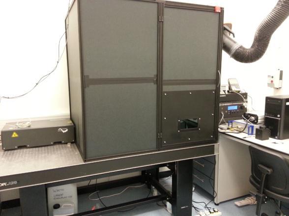
8 Curing polymers in situ Simultaneous curing and sintering mechanisms Power socket Heating element (reached 180 C) Ceramic thermal insulator


9 Example End Goal - Incorporated electronics and printed interconnect Current Aim: Incorporating electronic components and inkjet printed conductive tracks inside 3D printed structures Printed interconnecting tracks embedded Rechargeable battery Resistor LED Switch
10 Major Challenges Material Ink conductivity Dielectric ink stability Thermal / Chemical / Structural Ink drying Height Mismatch System Multiple BMP More than two materials Curing Mechanism Sintering Temperatures Print head control cooling!
11 Enabling Complex products Multifunctional, multimaterial products Graded products Resolution < 50mm
12 Contents 3D Printing at Nottingham: EPSRC Centre for Innovative Manufacturing in Additive Manufacturing Ink jet printing Opportunities in healthcare Nano scale


13 2D array printing: a novel concept for oral dosage form manufacture


14 3D Printing: Extrusion of solid dosage forms Extrusion based 3D printer setup for dual material deposition

15 Going further: Printed bilayer structures
 Cured using UV illumination Initiators include Type 1: Irgacure 2959 Type 2: Photoinitiator: 2,4- Diethyl-9H-thioxanthen-9- one Accelerator: Ethyl 4- (dimethylamino)benzoate")
16 Getting better control: Ink jet printing bioresorbable materials Development of PCL(DA) as a UV curable bioresorbable ink (polycaprolactone macromer with diacrylate functional groups at the ends for UV driven cross-linking) Cured using UV illumination Initiators include Type 1: Irgacure 2959 Type 2: Photoinitiator: 2,4- Diethyl-9H-thioxanthen-9- one Accelerator: Ethyl 4- (dimethylamino)benzoate 4mm 10 Layers UV cured PCLDA-PEGDA ink (PCLDA:PEGDA=60%:40%, Droplet Spacing=40μm, Thickness=55 μm)


17 Demonstrating complexity
18 Ink jet printing enabling multifunctional Multifunctional means Structural, sensing, actuation for biomedical devices Structural, active pharma ingredient for drug delivery systems
19 Contents 3D Printing at Nottingham: EPSRC Centre for Innovative Manufacturing in Additive Manufacturing Ink jet printing Opportunities in healthcare Nano scale


20 System Design Based on Multi photon microscopy system


21 Multi-photon polymerisation system Material: OrmoComp Laser: Coherent Chameleon Ultra II, 780 nm, 80 MHz, 48 mw 100x oil-immersion lens, scanning speed 10 µm/s Before developing Video: Scan a Video: Scan b After developing 10 µm 250 µm 27 layers 500 nm/layer

22 Why NANOS? Smart micropatterned neural interfaces Collaboration with Electrical Engineering and Biology The aim is to fabricate a sensor platform to investigate neural information processing Neural Interface: Allows for bidirectional communication between neural tissue and a computer. In vitro: in glass, outside the body Goal: Build a platform for investigating the information processing of neural networks.
 Manufacture of structures")


23 Enhancing MPP with Optical Trapping Aim to manufacture double negative meta-materials using multi-photon polymerisation and optical trapping (OT) Manufacture of structures with different physical and electro-magnetic properties combining MPP and OT Fabrication of meta-material structures within a wider electromagnetic frequency range (into the visible) Combination of optical trapping techniques with MPP rig to produce a system capable of manoeuvring active elements within a structure Initiated with a single, low power, OT system
24 Nano scale 3D Printing Structures with feature sizes <100nm Multimaterial devices on the nano scale Hybridisation means integration of length scales (e.g., with optical tweezers) Sensors (bio, opto)
25 Recent Award Great Technologies EPSRC Equipment Call Successful in obtaining 2.7Million for Equipment Multimaterial AM MetalJet Jetting of metallic droplets from 2000 degc with Oce JetMax 6 head jetting system with multiple material conversion routes 200mm build height NANOS+ - Multi-material 2PP system with multi-beam optical control and placement Analytical ToF SIMS upgrade (with Pharmacy) AFM upgrade (with Pharmacy)
26 Centre for Doctoral Training in AM and 3D Printing Centre for Doctoral Training Specific AM training for PhD 70 PhD students over 5 years Four partners, Liverpool, Newcastle and Loughborough Bespoke training programme for basic AM training prior to PhD work Industry-base utilised for directing teaching activities Internships in companies Professional Environment Study Tours Industry partners providing 30-45k per student for enhanced stipend/travel and consumables October 2014 start date
27 Acknowledgements Big thanks to: Chris Tuck Bochuan Liu Ehab Saleh Yinfeng He Clive Roberts Morgan Alexander Sam Kilsby (Lboro) Steve Christie (Lboro) Steve Edmondson (Lboro) Mark East Mark Hardy Richard Hague Ian Ashcroft Marcel Slot (Oce) Qin Hu Meisam Askari Astra-Zeneca
28 Any Questions? Any Questions? Prof. Ricky Wildman e: w: w:
Passive Direct Print Sensors
 Passive Wireless Sensor Technology Workshop June 6-7, 2012 Hyatt Regency, La Jolla, CA Passive Direct Print Sensors Mike Newton mnewton@nscrypt.com nscrypt Inc. Orlando, Florida University of Texas at
Supplementary Information
 Supplementary Information Dynamic manipulation and separation of individual semiconducting and metallic nanowires Arash Jamshidi 1, Peter J. Pauzauskie 2,3, P. James Schuck 4, Aaron T. Ohta 1, Pei-Yu Chiou
MICROFLEX Project: MEMS on New Emerging Smart Textiles/Flexibles
 MICROFLEX Project: MEMS on New Emerging Smart Textiles/Flexibles S Beeby, M J Tudor, R Torah, K Yang, Y Wei Dr Steve Beeby ESD Research Group Smart Fabrics 2011 5 th April 2011 Overview Introduce the MicroFlex
Advances in Multimaterial and Multifunctional Additive Manufacturing
 Advances in Multimaterial and Multifunctional Additive Manufacturing Final Report April 2017 Contents 4 Our ambition achieved 6 Defining Multifunctional Additive Manufacturing: the next generation 8 Executive
MID Manufacturing Process.
 3D Aerosol Jet Printing An Emerging MID Manufacturing Process. Dr. Martin Hedges Neotech Services MTP, Nuremberg, Germany info@neotechservices.com Aerosol Jet Printing Aerosol Jet Process Overview Current
National Centre for Flexible Electronics
 National Centre for Flexible Electronics Tripartite Partnership Government FlexE Centre - A platform for a meaningful interaction between industry and academia. An interdisciplinary team that advances
Figure 7 Dynamic range expansion of Shack- Hartmann sensor using a spatial-light modulator
 Figure 4 Advantage of having smaller focal spot on CCD with super-fine pixels: Larger focal point compromises the sensitivity, spatial resolution, and accuracy. Figure 1 Typical microlens array for Shack-Hartmann
Femtosecond laser microfabrication in. Prof. Dr. Cleber R. Mendonca
 Femtosecond laser microfabrication in polymers Prof. Dr. Cleber R. Mendonca laser microfabrication focus laser beam on material s surface laser microfabrication laser microfabrication laser microfabrication
Lecture 22 Optical MEMS (4)
") EEL6935 Advanced MEMS (Spring 2005) Instructor: Dr. Huikai Xie Lecture 22 Optical MEMS (4) Agenda: Refractive Optical Elements Microlenses GRIN Lenses Microprisms Reference: S. Sinzinger and J. Jahns,
EEL6935 Advanced MEMS (Spring 2005) Instructor: Dr. Huikai Xie Lecture 22 Optical MEMS (4) Agenda: Refractive Optical Elements Microlenses GRIN Lenses Microprisms Reference: S. Sinzinger and J. Jahns,
The Power of Print in Laminated Card Manufacturing
 The Power of Print in Laminated Card Manufacturing ICMA EuroForum 2014-9 th / 10 th October Robin McMillan & John Schneiderhan working for you. Overview Current print processes and related inks Introduction
1.8.3 Haptic-Based CAD 1.9 About this Book 1.10 Exercises References Development of Additive Manufacturing Technology
 Contents 1 Introduction and Basic Principles 1 1.1 What Is Additive Manufacturing? 1 1.2 What Are AM Parts Used for? 3 1.3 The Generic AM Process 4 1.3.1 Step 1: CAD 4 1.3.2 Step 2: Conversion to STL 4
EMERGING INKJET PRINTING TECHNOLOGIES, APPLICATIONS AND GLOBAL MARKETS
 EMERGING INKJET PRINTING TECHNOLOGIES, APPLICATIONS AND GLOBAL MARKETS AVM091B November 2014 Andrew McWilliams Project Analyst ISBN: 1-56965-999-0 BCC Research 49 Walnut Park, Building 2 Wellesley, MA
Low Temperature Integration of Thin Films and Devices for Flexible and Stretchable Electronics
 Low Temperature Integration of Thin Films and Devices for Flexible and Stretchable Electronics Pooran Joshi, Stephen Killough, and Teja Kuruganti Oak Ridge National Laboratory FIIW 2015 Displays and PV
Digital low migration printing Technology status and benefits
 Digital low migration printing Technology status and benefits Roel De Mondt, PhD Agfa Gevaert N.V. Belgium Packaging and Can Coatings - June 2013 - Dusseldorf Outline Organisation Short background on inkjet
Double Emulsion Chip (100 μm etch depth), water-oil-water Part No
, water-oil-water Part No") Unit 1, Anglian Business Park, Orchard Road, Royston, Hertfordshire, SG8 5TW, UK T: +44 (0)1763 242491 F: +44 (0)1763 246125 E: sales@dolomite-microfluidics.com W: www.dolomite-microfluidics.com Dolomite
Unit 1, Anglian Business Park, Orchard Road, Royston, Hertfordshire, SG8 5TW, UK T: +44 (0)1763 242491 F: +44 (0)1763 246125 E: sales@dolomite-microfluidics.com W: www.dolomite-microfluidics.com Dolomite
Projects and Partners Working with Chalcogenide Advanced Manufacturing Partnership (ChAMP)
") Projects and Partners Working with Chalcogenide Advanced Manufacturing Partnership (ChAMP) Dr John Lincoln Industrial Liaison Officer j.lincoln@soton.ac.uk March 2015 ChAMP Aims Establish world leading
Projects and Partners Working with Chalcogenide Advanced Manufacturing Partnership (ChAMP) Dr John Lincoln Industrial Liaison Officer j.lincoln@soton.ac.uk March 2015 ChAMP Aims Establish world leading
Visual Imaging in the Electronic Age
 Visual Imaging in the Electronic Age ART 2107, ARCH 3702, CS 1620, ENGRI 1620 3D Printing October 20, 2015 Prof. Donald P. Greenberg dpg5@cornell.edu Types of 3D Printers Selective deposition printers
Optimisation of Substrate Angles for Three Dimensional Inkjet Printing of multifunctional
 Optimisation of Substrate Angles for Three Dimensional Inkjet Printing of multifunctional and multi-material parts Jayasheelan Vaithilingam*, Kasidis Laoboonmee, Ehab Saleh, Richard J.M. Hague, Ricky D.
3D and Aerosol Printed Conductor Dielectric Full- 3D RF Metamaterials
 3D and Aerosol Printed Conductor Dielectric Full- 3D RF Metamaterials June 22, 2017 Jimmy Hester, Evan Nguyen, Jesse Tice, and Vesna Radisic Approved for Public Release: NG17-1180, 6/2/17 Outline Introduction
Supporting Information
 Supporting Information Free-Standing Photonic Crystal Films with Gradient Structural Colors Haibo Ding, Cihui Liu, Baofen Ye, Fanfan Fu, Huan Wang, Yuanjin Zhao*, Zhongze Gu* State Key Laboratory of Bioelectronics,
Sensors and Metrology - 2 Optical Microscopy and Overlay Measurements
 Sensors and Metrology - 2 Optical Microscopy and Overlay Measurements 1 Optical Metrology Optical Microscopy What is its place in IC production? What are the limitations and the hopes? The issue of Alignment
Drop-on-Demand Inkjet Printing of Liquid Crystals for Photonics Applications
 Drop-on-Demand Inkjet Printing of Liquid Crystals for Photonics Applications Ellis Parry, Steve Elston, Alfonson Castrejon-Pita, Serena Bolis and Stephen Morris PhD Student University of Oxford Drop-on
Standard Operating Procedure of Atomic Force Microscope (Anasys afm+)
") Standard Operating Procedure of Atomic Force Microscope (Anasys afm+) The Anasys Instruments afm+ system incorporates an Atomic Force Microscope which can scan the sample in the contact mode and generate
Standard Operating Procedure of Atomic Force Microscope (Anasys afm+) The Anasys Instruments afm+ system incorporates an Atomic Force Microscope which can scan the sample in the contact mode and generate
Visual Imaging in the Electronic Age
 Visual Imaging in the Electronic Age ART 2107, ARCH 3702, CS 1620, ENGRI 1620 3D Printing November 6, 2014 Prof. Donald P. Greenberg dpg5@cornell.edu Types of 3D Printers Selective deposition printers
CREST Cluster Focus & Projects. 23rd February 2015
 CREST Cluster Focus & Projects 23rd February 2015 Domain Areas Clusters focus 1. Optoelectronics/LED and Solid State Lighting 2. Embedded System & Internet of Things 3. IC Design, Test & Validation 4.
New Horizons. A new paradigm. of collaborative research
 New Horizons A new paradigm of collaborative research One of the immediate and complex challenges facing industry, business and government in Australia today is a need to increase exports, foreign investment
Effect of Corona Treatment on Spreading Behavior of UV Ink over Inkjet Printed Silver Nano-Particle Layer
 Effect of Corona Treatment on Spreading Behavior of UV Ink over Inkjet Printed Silver Nano-Particle Layer Khushbeen Department of Printing Technology GJUS&T, Hisar, Haryana, India Email- khushveen12@gmail.com
BioInstrumentation Laboratory
 BioInstrumentation Laboratory Ian Hunter Vienna, May 22 2013 BioInstrumentation Lab, Mechanical Engineering, MIT - Robotic endoscopes - Needle-free drug delivery devices - Eye micro-surgery robots - High
MEMS in ECE at CMU. Gary K. Fedder
 MEMS in ECE at CMU Gary K. Fedder Department of Electrical and Computer Engineering and The Robotics Institute Carnegie Mellon University Pittsburgh, PA 15213-3890 fedder@ece.cmu.edu http://www.ece.cmu.edu/~mems
EPD ENGINEERING PRODUCT DEVELOPMENT
 EPD PRODUCT DEVELOPMENT PILLAR OVERVIEW The following chart illustrates the EPD curriculum structure. It depicts the typical sequence of subjects. Each major row indicates a calendar year with columns
Fieldlab Multi-material 3D Printing 3D printed structural electronics at TNO AMSYSTEMS Center
 Fieldlab Multi-material 3D Printing 3D printed structural electronics at TNO AMSYSTEMS Center Dr. Wijnand Germs wijnand.germs@tno.nl 3DP STRUCTURAL ELECTRONICS DEMO STATUS TODAY 3DP STRUCTURAL ELECTRONICS
Where the brightest scientific minds thrive. IMED Early Talent and Post Doc programmes
 Where the brightest scientific minds thrive. IMED Early Talent and Post Doc programmes Scientific innovation is at the heart of everything we do. Scientific innovation is at the heart of our business and
Micro-sensors - what happens when you make "classical" devices "small": MEMS devices and integrated bolometric IR detectors
 Micro-sensors - what happens when you make "classical" devices "small": MEMS devices and integrated bolometric IR detectors Dean P. Neikirk 1 MURI bio-ir sensors kick-off 6/16/98 Where are the targets
The Shape of Things to Come Strategies for Success in the Age of 3D Printing. Husch Blackwell LLP
 The Shape of Things to Come Strategies for Success in the Age of 3D Printing Husch Blackwell LLP What is 3D Printing and How Does it Work? State of 3D Printing As of 2014: 80,000 industrial printers worldwide
UV TECHNOLOGY. Relatively new, but rapidly emerging technology. AZON Q UV PRODUCT CATALOG
 UV TECHNOLOGY Relatively new, but rapidly emerging technology. UV curing has been widely adopted in many industries including automotive, telecommunications, electronics, graphic arts, converting and metal,
EPD ENGINEERING PRODUCT DEVELOPMENT
 EPD PRODUCT DEVELOPMENT PILLAR OVERVIEW The following chart illustrates the EPD curriculum structure. It depicts the typical sequence of subjects. Each major row indicates a calendar year with columns
shaping global nanofuture ULTRA-PRECISE PRINTING OF NANOMATERIALS
 shaping global nanofuture ULTRA-PRECISE PRINTING OF NANOMATERIALS WHO ARE WE? XTPL S.A. is a company operating in the nanotechnology segment. The interdisciplinary team of XTPL develops on a global scale
NON-TRADITIONAL MACHINING PROCESSES ULTRASONIC, ELECTRO-DISCHARGE MACHINING (EDM), ELECTRO-CHEMICAL MACHINING (ECM)
, ELECTRO-CHEMICAL MACHINING (ECM)") NON-TRADITIONAL MACHINING PROCESSES ULTRASONIC, ELECTRO-DISCHARGE MACHINING (EDM), ELECTRO-CHEMICAL MACHINING (ECM) A machining process is called non-traditional if its material removal mechanism is basically
NON-TRADITIONAL MACHINING PROCESSES ULTRASONIC, ELECTRO-DISCHARGE MACHINING (EDM), ELECTRO-CHEMICAL MACHINING (ECM) A machining process is called non-traditional if its material removal mechanism is basically
Midaz Micro-Slab DPSS Lasers:
 Midaz Micro-Slab DPSS Lasers: Higher power & pulse rate for higher speed micromachining Professor Mike Damzen Midaz Laser Ltd 4 June 2008 AILU Meeting Industrial opportunities in laser micro and nano processing
INTEGRATED OPTICAL AND ELECTRONIC INTERCONNECT PCB MANUFACTURING (OPCB)
") INTEGRATED OPTICAL AND ELECTRONIC INTERCONNECT PCB MANUFACTURING (OPCB) IeMRC FLAGSHIP PROJECT IeMRC Annual Conference Loughborough 4 th July 2008 PROJECT OBJECTIVES 1. Enhance fabrication techniques for
INTEGRATED OPTICAL AND ELECTRONIC INTERCONNECT PCB MANUFACTURING (OPCB) IeMRC FLAGSHIP PROJECT IeMRC Annual Conference Loughborough 4 th July 2008 PROJECT OBJECTIVES 1. Enhance fabrication techniques for
Design & Simulation of Multi Gate Piezoelectric FET Devices for Sensing Applications
 Design & Simulation of Multi Gate Piezoelectric FET Devices for Sensing Applications Sunita Malik 1, Manoj Kumar Duhan 2 Electronics & Communication Engineering Department, Deenbandhu Chhotu Ram University
FUJIFILM Dimatix Technology Integration:
 News Release Editorial Contact: Edward Chrusciel FUJIFILM Dimatix 603-443-5364 echrusciel@dimatix.com FOR IMMEDIATE RELEASE FUJIFILM Dimatix Technology Integration: Helping companies incorporate the power
Making business with E-printing
 Making business with E-printing Erik Teunissen BERENSCHOT 1 SRWC Abstract The transfer of new technologies to the market consumes more time and effort than we think off. The main issues to be successful
NTU RECIPIENTS OF NRF S PROOF OF CONCEPT SCHEME GRANTS. 1. A Semantics-Based and Service-Oriented Framework for the Virtualisation of Sensor Networks
 Reg. No. 200604393R FACT SHEET For immediate release Total: 7 pages including this page Singapore, 21 August 2009 NTU RECIPIENTS OF NRF S PROOF OF CONCEPT SCHEME GRANTS 1. A Semantics-Based and Service-Oriented
Advanced Technology Solutions. Microwave Materials
 Advanced Technology Solutions Microwave Materials BAE SYSTEMS is an international company engaged in the development, delivery and support of advanced defence systems in the air, on land, at sea and in
INDIAN INSTITUTE OF TECHNOLOGY BOMBAY
 IIT Bombay requests quotations for a high frequency conducting-atomic Force Microscope (c-afm) instrument to be set up as a Central Facility for a wide range of experimental requirements. The instrument
Nanoscale Lithography. NA & Immersion. Trends in λ, NA, k 1. Pushing The Limits of Photolithography Introduction to Nanotechnology
 15-398 Introduction to Nanotechnology Nanoscale Lithography Seth Copen Goldstein Seth@cs.cmu.Edu CMU Pushing The Limits of Photolithography Reduce wavelength (λ) Use Reducing Lens Increase Numerical Aperture
Printing as a material deposition process
 Printing as a material deposition process Printing Materials, Mumbai 5 th March 2011 Prof. Fritz Bircher, www.printtechnology.ch 1 Presentation outline Material deposition The inkjet printing process Interaction
Accelerating Scale Up of Large Area Electronics
 Accelerating Scale Up of Large Area Electronics Duncan Lindsay Business Development Director, CPI 2015 Centre for Process Innovation Limited. All Rights Reserved. Who are CPI? CPI is a UK technology innovation
A miniature all-optical photoacoustic imaging probe
 A miniature all-optical photoacoustic imaging probe Edward Z. Zhang * and Paul C. Beard Department of Medical Physics and Bioengineering, University College London, Gower Street, London WC1E 6BT, UK http://www.medphys.ucl.ac.uk/research/mle/index.htm
Optical Waveguides fabricated by combination of ink-jet and flexographic printing
 Optical Waveguides fabricated by combination of ink-jet and flexographic printing P. Bollgrün 1,3, T. Wolfer 2, U. Gleissner 3 D. Mager 1, C. Megnin 3 T. Hanemann 3,4, L. Overmeyer 2, J. Korvink 1 1) Institute
AIR-COUPLED PHOTOCONDUCTIVE ANTENNAS
 AIR-COUPLED PHOTOCONDUCTIVE ANTENNAS Report: Air-Coupled Photoconductive Antennas In this paper, we present air-coupled terahertz photoconductive antenna (THz-PCAs) transmitters and receivers made on high-resistive
MEDIA RELEASE FOR IMMEDIATE RELEASE 26 JULY 2016
 MEDIA RELEASE FOR IMMEDIATE RELEASE 26 JULY 2016 A*STAR S IME KICKS OFF CONSORTIA TO DEVELOP ADVANCED PACKAGING SOLUTIONS FOR NEXT-GENERATION INTERNET OF THINGS APPLICATIONS AND HIGH-PERFORMANCE WIRELESS
Bring the Challenge. We ll Build the Solution.
 VISIONARY Bring the Challenge. We ll Build the Solution. Solving complex engineering challenges in a global market, Celera Motion advances the field and science of motion control. Our precision components
Additive Manufacturing Education in the UK
 Additive Manufacturing Education in the UK Phill Dickens Loughborough University Phill Reeves Econolysts Ltd. Richard Hague University of Nottingham Introduction There has been and continues to be a considerable
System demonstrator for board-to-board level substrate-guided wave optoelectronic interconnections
 Header for SPIE use System demonstrator for board-to-board level substrate-guided wave optoelectronic interconnections Xuliang Han, Gicherl Kim, Hitesh Gupta, G. Jack Lipovski, and Ray T. Chen Microelectronic
Plan Optik AG. Plan Optik AG PRODUCT CATALOGUE
 Plan Optik AG Plan Optik AG PRODUCT CATALOGUE 2 In order to service the high demand of wafers more quickly, Plan Optik provides off the shelf products in sizes from 2 up to 300mm diameter. Therefore Plan
Single Frequency DPSS Lasers
 Single Frequency DPSS Lasers Any wavelength from NIR to UV using a single engineering platform based on our proprietary patented BRaMMS DPSS Laser technology. We develop and produce Single Frequency DPSS
NanoFabrication Kingston. Seminar and Webinar January 31, 2017 Rob Knobel Associate Professor, Dept. of Physics Queen s University
 NanoFabrication Kingston Seminar and Webinar January 31, 2017 Rob Knobel Associate Professor, Dept. of Physics Queen s University What is NFK? It s a place, an team of experts and a service. The goal of
Inkjet Filling of TSVs with Silver Nanoparticle Ink. Behnam Khorramdel, Matti Mäntysalo Tampere University of Technology ESTC 2014 Finland, Helsinki
 Inkjet Filling of TSVs with Silver Nanoparticle Ink Behnam Khorramdel, Matti Mäntysalo Tampere University of Technology ESTC 2014 Finland, Helsinki Outline Motivation for this study Inkjet in MEMS fabrication
Printed and Hybrid Integration
 Printed and Hybrid Integration Neil Chilton PhD Technical Director, Printed Electronics Limited, UK Neil.Chilton@PrintedElectronics.com Printed Electronics Limited (PEL) General Overview PEL was founded
Small Droplet Chips. product datasheet
 Unit 1, Anglian Business Park, Orchard Road, Royston, Hertfordshire, SG8 5TW, UK T: +44 (0)1763 242491 F: +44 (0)1763 246125 E: sales@dolomite-microfluidics.com W: www.dolomite-microfluidics.com Small
:... resolution is about 1.4 μm, assumed an excitation wavelength of 633 nm and a numerical aperture of 0.65 at 633 nm.
 PAGE 30 & 2008 2007 PRODUCT CATALOG Confocal Microscopy - CFM fundamentals :... Over the years, confocal microscopy has become the method of choice for obtaining clear, three-dimensional optical images
Supporting Materials for. A Novel Color Modulation Analysis Strategy. through Tunable Multiband Laser for. Nanoparticle Identification and Evaluation
 Supporting Materials for A Novel Color Modulation Analysis Strategy through Tunable Multiband Laser for Nanoparticle Identification and Evaluation Xuan Cao,, Gang Lei, Jingjing Feng, Qi Pan, Xiaodong Wen,
Scientific Highlights 2016
 Scientific Highlights 2016 Science and Technology Sector Schools and Faculties Faculty of Science Louvain School of Engineering (EPL) Faculty of Architecture, Architectural Engineering and Urban Planning
Just where it s needed
 Seite/Page: 1 Just where it s needed Continuing miniaturisation of many products requires a method of dispensing very small amounts of liquids Inkjet technology is capable of applying adhesives and many
The Shape of Things to Come Strategies for Success in the Age of 3D Printing. Husch Blackwell LLP
 The Shape of Things to Come Strategies for Success in the Age of 3D Printing Husch Blackwell LLP What is 3D Printing and How Does it Work? State of 3D Printing 1. As of 2014: 80,000 industrial printers
Photonic device package design, assembly and encapsulation.
 Photonic device package design, assembly and encapsulation. Abstract. A.Bos, E. Boschman Advanced Packaging Center. Duiven, The Netherlands Photonic devices like Optical transceivers, Solar cells, LED
Des MEMS aux NEMS : évolution des technologies et des concepts aux travers des développements menés au LETI
 Des MEMS aux NEMS : évolution des technologies et des concepts aux travers des développements menés au LETI Ph. Robert 1 Content LETI at a glance From MEMS to NEMS: 30 years of technological evolution
Agilent Cary 610/620 FTIR microscopes and imaging systems RESOLUTION FOR EVERY APPLICATION
 Agilent Cary 610/620 FTIR microscopes and imaging systems RESOLUTION FOR EVERY APPLICATION AGILENT CARY 610/620 FTIR MICROSCOPES ADVANCING FTIR MICROSCOPY AND IMAGING Agilent s 610/620 FTIR microscopes
Micro-PackS, Technology Platform. Security Characterization Lab Opening
 September, 30 th 2008 Micro-PackS, Technology Platform Security Characterization Lab Opening Members : Micro-PackS in SCS cluster From Silicium to innovative & commucating device R&D structure, gathering
Aerosol Jet Printing of Structured Films. Denis Cormier Rochester Institute of Technology
 Aerosol Jet Printing of Structured Films Denis Cormier Rochester Institute of Technology cormier@mail.rit.edu Metal additive manufacturing of engineered titanium lattice structures Local control over strength,
School of Instrument Science and Opto-electronics Engineering, Hefei University of Technology, Hefei, China 2
 59 th ILMENAU SCIENTIFIC COLLOQUIUM Technische Universität Ilmenau, 11 15 September 2017 URN: urn:nbn:de:gbv:ilm1-2017iwk-009:9 Low-Frequency Micro/Nano-vibration Generator Using a Piezoelectric Actuator
Ultrafast Beams and Applications UBA July, 2017 Presenter: Arsham Yeremyan
 Laser driven facility for irradiation experiments, two-photon microscopy and microfabrication Ultrafast Beams and Applications UBA17 04-07 July, 2017 Presenter: Arsham Yeremyan Outline Parallel operation
Brillia HD Pro-T3. A new era in print demands a new era in platemaking. A huge global user base. The most advanced printing plate ever
 Brillia HD PRO-T3 represents Fujifilm s most advanced printing plate to date, featuring high performance technologies that deliver groundbreaking performance. A new era in print demands a new era in platemaking
PILOT LINE FOR LARGE-AREA PRINTING OF ELECTRONIC AND PHOTONIC DEVICES. Simon Perraud, Ph.D. Vice president for European affairs
 PILOT LINE FOR LARGE-AREA PRINTING OF ELECTRONIC AND PHOTONIC DEVICES Simon Perraud, Ph.D. Vice president for European affairs ABOUT LITEN Liten is the research institute of CEA devoted to clean energy
Optical Bus for Intra and Inter-chip Optical Interconnects
 Optical Bus for Intra and Inter-chip Optical Interconnects Xiaolong Wang Omega Optics Inc., Austin, TX Ray T. Chen University of Texas at Austin, Austin, TX Outline Perspective of Optical Backplane Bus
Introduction to Microdevices and Microsystems
 PHYS 534 (Fall 2008) Module on Microsystems & Microfabrication Lecture 1 Introduction to Microdevices and Microsystems Srikar Vengallatore, McGill University 1 Introduction to Microsystems Outline of Lecture
Dr. Charles Watt. Educational Advancement & Innovation
 Dr. Charles Watt Educational Advancement & Innovation 1 21st Century Education What are the critical skills our undergraduate students need? Technical depth in a particular field Creativity and innovation
PicoMaster 100. Unprecedented finesse in creating 3D micro structures. UV direct laser writer for maskless lithography
 UV direct laser writer for maskless lithography Unprecedented finesse in creating 3D micro structures Highest resolution in the market utilizing a 405 nm diode laser Structures as small as 300 nm 375 nm
Processes for Flexible Electronic Systems
 Processes for Flexible Electronic Systems Michael Feil Fraunhofer Institut feil@izm-m.fraunhofer.de Outline Introduction Single sheet versus reel-to-reel (R2R) Substrate materials R2R printing processes
Refractive Microlens Fabrication by Ink-Jet Process
 Refractive Microlens Fabrication by Ink-Jet Process S. BIEHL, R. DANZEBRINK, P. OLIVEIRA AND M.A. AEGERTER Institut für Neue Materialien-INM, Department of Coating Technology, Im Stadtwald 43, D-66123
Laser Speckle Reducer LSR-3000 Series
 Datasheet: LSR-3000 Series Update: 06.08.2012 Copyright 2012 Optotune Laser Speckle Reducer LSR-3000 Series Speckle noise from a laser-based system is reduced by dynamically diffusing the laser beam. A
attocfm I for Surface Quality Inspection NANOSCOPY APPLICATION NOTE M01 RELATED PRODUCTS G
 APPLICATION NOTE M01 attocfm I for Surface Quality Inspection Confocal microscopes work by scanning a tiny light spot on a sample and by measuring the scattered light in the illuminated volume. First,
Performance of High Pixel Density Multi-anode Microchannel Plate Photomultiplier tubes
 Performance of High Pixel Density Multi-anode Microchannel Plate Photomultiplier tubes Thomas Conneely R&D Engineer, Photek LTD James Milnes, Jon Lapington, Steven Leach 1 page 1 Company overview Founded
The Department of Advanced Materials Engineering. Materials and Processes in Polymeric Microelectronics
 The Department of Advanced Materials Engineering Materials and Processes in Polymeric Microelectronics 1 Outline Materials and Processes in Polymeric Microelectronics Polymeric Microelectronics Process
CREATE PROJECT Edit Printer. Tutorial_V2 - Updated: 13,0600,1489,1629(SP6)
") CREATE PROJECT Tutorial_V2 - Updated: 13,0600,1489,1629(SP6) In this exercise, we will learn how to edit the printer! Notice/ Remember Left mouse button name is "pick" Middle mouse button name is "Exit"
CREATE PROJECT Tutorial_V2 - Updated: 13,0600,1489,1629(SP6) In this exercise, we will learn how to edit the printer! Notice/ Remember Left mouse button name is "pick" Middle mouse button name is "Exit"
Optical signal processing for fiber Bragg grating based wear sensors
 University of Wollongong Research Online Faculty of Informatics - Papers (Archive) Faculty of Engineering and Information Sciences 2005 Optical signal processing for fiber Bragg grating based wear sensors
Open Innovation to Manage Risks in Technology The Business of Breakthroughs
 Open Innovation to Manage Risks in Technology The Business of Breakthroughs Janos Veres, Program Manager 2016 PARC, All rights reserved. PARC Legacy: A Storied History of Inventing the Future 1970 1973
Module 11: Photolithography. Lecture 14: Photolithography 4 (Continued)
") Module 11: Photolithography Lecture 14: Photolithography 4 (Continued) 1 In the previous lecture, we have discussed the utility of the three printing modes, and their relative advantages and disadvantages.
Module 11: Photolithography Lecture 14: Photolithography 4 (Continued) 1 In the previous lecture, we have discussed the utility of the three printing modes, and their relative advantages and disadvantages.
New applications are transforming the UV-LED market, and Nikkiso Deep UV-LED devices are applicable to many important applications including:
 LED Ultraviolet Light Emitting Diodes (UV-LED) Nikkiso s advantaged UV-LED products all with high performance and reliability at an affordable cost. Along with our sglux UV sensors and probes, Boston Electronics
A Novel Surgery-like Strategy for Droplet Coalescence in Microchannels
 Supplementary Material (ESI) for Lab on a Chip A Novel Surgery-like Strategy for Droplet Coalescence in Microchannels Supplementary material Nan-Nan Deng, a Shao-Xing Sun, a Wei Wang, a Xiao-Jie Ju, a
Droplet Junction Chips
 Unit 1, Anglian Business Park, Orchard Road, Royston, Hertfordshire, SG8 5TW, UK T: +44 (0)1763 242491 F: +44 (0)1763 246125 E: sales@dolomite-microfluidics.com W: www.dolomite-microfluidics.com Dolomite
LMT F14. Cut in Three Dimensions. The Rowiak Laser Microtome: 3-D Cutting and Imaging
 LMT F14 Cut in Three Dimensions The Rowiak Laser Microtome: 3-D Cutting and Imaging The Next Generation of Microtomes LMT F14 - Non-contact laser microtomy The Rowiak laser microtome LMT F14 is a multi-purpose
Anapurna H3200i LED.
 The is a high-speed hybrid UV LED-curable inkjet system with a printing width of 3.2 m for indoor and outdoor applications. www.agfagraphics.com The is a high-speed hybrid UV LED-curable inkjet system
Electronics the hidden sector. Dr Kathryn Walsh Director, Electronics-enabled Products KTN
 Electronics the hidden sector Dr Kathryn Walsh Director, Electronics-enabled Products KTN Here to celebrate! The projects The Innovative electronics Manufacturing Research Centre The Industry! Why hidden?
Simple & Perfect Wide format UV-curable flatbed inkjet printer
 Simple & Perfect Wide format UV-curable flatbed inkjet printer Coming SOON KX7 / KX7-R Large Flatbed with RtoR option New JETRIX KX7 series, Coming with Reliable quality & productivity & functionality
Asia Microreactors Datasheet
 System : Asia Module : Microreactors Version :.0 Date : 7 th February 0 Created/ Revised by : Maxime Drobot Asia Microreactors Datasheet This document provides specifications and information for Syrris
TRAINING MANUAL. Multiphoton Microscopy LSM 510 META-NLO
 TRAINING MANUAL Multiphoton Microscopy LSM 510 META-NLO September 2010 Multiphoton Microscopy Training Manual Multiphoton microscopy is only available on the LSM 510 META-NLO system. This system is equipped
GLOBAL MARKETS, TECHNOLOGIES AND MATERIALS FOR THIN AND ULTRATHIN FILMS
 GLOBAL MARKETS, TECHNOLOGIES AND MATERIALS FOR THIN AND ULTRATHIN FILMS SMC057C August Margareth Gagliardi Project Analyst ISBN: 1-62296-338-5 BCC Research 49 Walnut Park, Building 2 Wellesley, MA 02481