Drop-on-Demand Inkjet Printing of Liquid Crystals for Photonics Applications
|
|
|
- Shanon Short
- 5 years ago
- Views:
Transcription
1 Drop-on-Demand Inkjet Printing of Liquid Crystals for Photonics Applications Ellis Parry, Steve Elston, Alfonson Castrejon-Pita, Serena Bolis and Stephen Morris PhD Student University of Oxford


 Lean,")
2 Drop-on demand Printing of Liquid Crystals Advantages of Inkjet Printing: Control of droplet properties and positioning Low temperature and fast Compatible with a range of substrates and fluids Unique geometries (free-form) Lean, efficient and flexible manufacturing 2

3 Experimental Set-up Custom Print head: Ink Heating Unit 1 Piezoelectric Transducer Nozzle Plate 3
4 Experimental Set-up 4

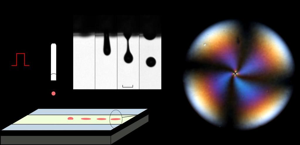
5 = Drop Formation 10% PVA 90V actuation wave 200μm nozzle diameter = 5

6 Drop Formation PVA 180V actuation wave 200μm nozzle diameter 6

7 Drop Formation PVA 90V actuation wave 200μm nozzle diameter 7

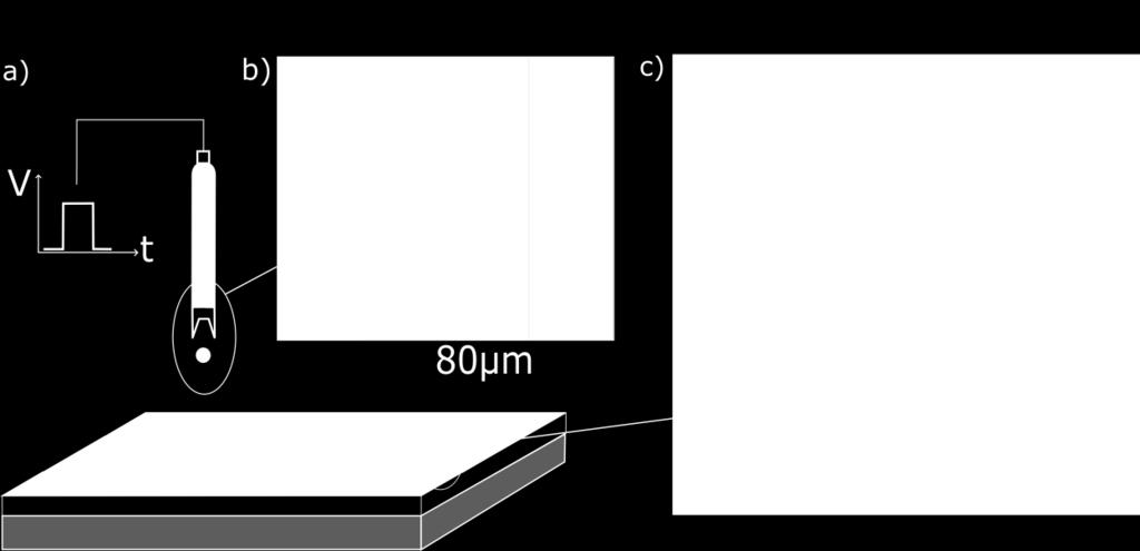
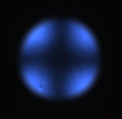
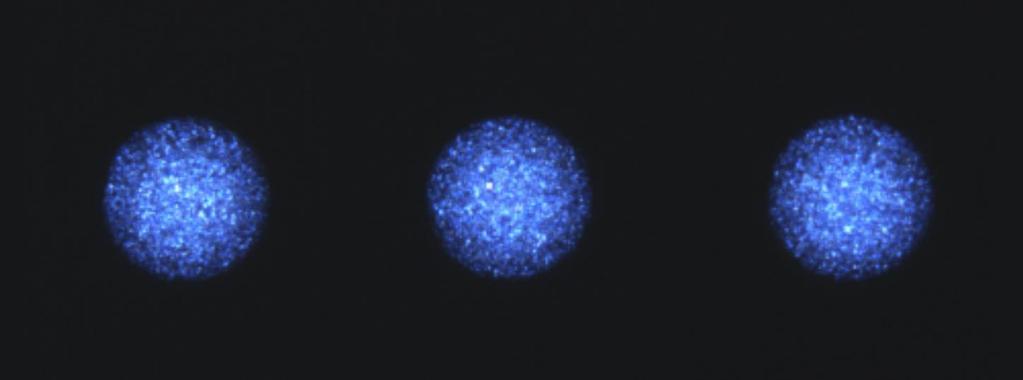
8 Experimental Set-up 75µm E7 Polarised Microscopy Images 100ms after deposition 8

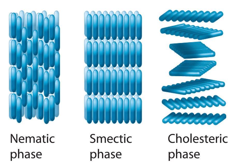
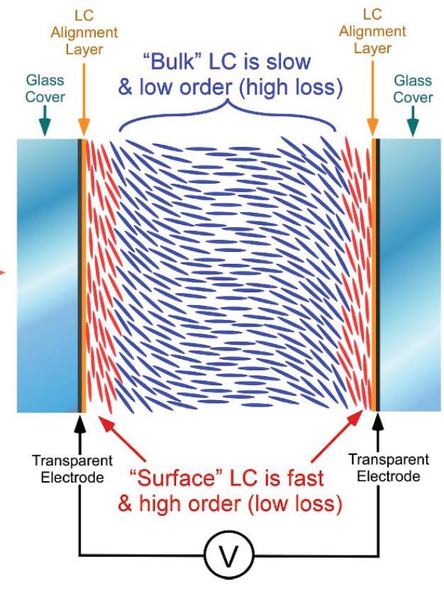
9 Liquid Crystals A Conventional Liquid Crystal Cell: 9
10 The Inkjet Printing of LCs 1. Reliable printing of fluid or ink 2. Formation of a defined droplet 3. Alignment of the LC Bare Glass 10


11 The Inkjet Printing of LCs 1. Reliable printing of fluid or ink 2. Formation of a defined droplet 3. Alignment of the LC Bare Glass Rubbed Polyamide Cell 11
 12")
12 Achieving LC Alignment Low molecular weight (10,000) PVA 80% Hydrolysed Wet layer 70µm deep (25µm when dry) E7 Nematic LC Dry PVA Bed Parry. E, Kim. D.J, Castrejón-Pita. A. A, Elston. S. J, Morris. M. M, Optical Materials (2018) 12
 13")
13 Achieving LC Alignment Low molecular weight (10,000) PVA 80% Hydrolysed Wet layer 70µm deep (25µm when dry) E7 Nematic LC Wet PVA Bed Parry. E, Kim. D.J, Castrejón-Pita. A. A, Elston. S. J, Morris. M. M, Optical Materials (2018) 13


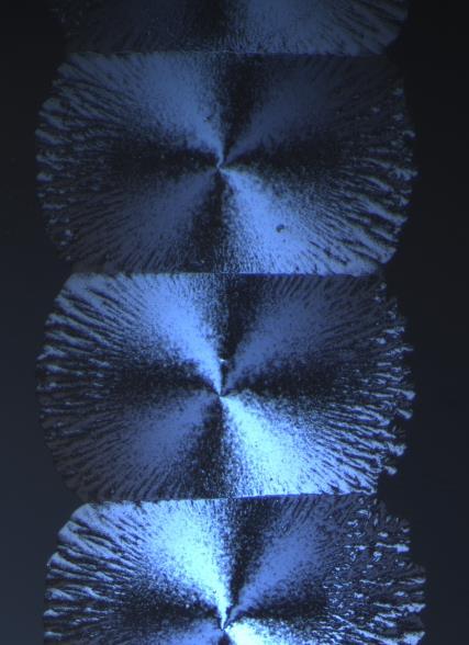
14 Achieving LC Alignment Partially Dry Polymer Bed Experimental Details: 70-90% drying time Defined droplet boundary Passive radial planar alignment achieved Resultant Droplets: Spherical droplet boundary Uniformity of the LC director Passive radial planar alignment achieved Parry. E, Kim. D.J, Castrejón-Pita. A. A, Elston. S. J, Morris. M. M, Optical Materials (2018) 14
 Increasing Temperature 0 350 Wavelength (nm) 800")
15 Transmission (%) CLC Temperature Sensors 95 BL006 + R811 (70:30) Increasing Temperature Wavelength (nm)

16 CLC Temperature Sensors 25 C 28 C 30 C 35 C 40 C 45 C 50 C 55 C 60 C 65 C 16


17 Microlens Arrays Applications Applications: Light collection Laser Arrays Photovoltaics 3D photography and displays Machine Vision Pixel Detector 17


18 Printing a Microlens < 10ms the droplet forms a stable shape Drop profile is spherical Bo << 1 for L < 1mm f 10ms α 70µm R 75µm drop diameter 1.5ms -1 drop velocity 18


19 Forming LC Microlenses α ß 70µm Standard 1xSurface 55µm Hydrophobic Surface f f 75µm drop diameter Hydrophobic Surface D D 19


20 Printing a Microlens α α α 70µm 1 drop 150µm 200µm 10 drops 20 drops f f f 75µm drop diameter 10 drops 3500Hz D D D 20
21 Liquid Crystal Microlens Determination of focal Length Intensity cross section at focal plane Polarisation independent focussing Parry. E, Bolis. S, Castrejón-Pita. A. A, Elston. S. J, Morris. M. M, Adv. Eng. Mat (2018) 21


22 Printing LC Microlens Arrays 100µm µm µm 75µm drop diameter E7 LC Array Homeotropic E7 Array of different sized Lenses Parry. E, Bolis. S, Castrejón-Pita. A. A, Elston. S. J, Morris. M. M, Adv. Eng. Mat (2018) 22


23 Microlens Arrays Thermal Tuning Parry. E, Bolis. S, Castrejón-Pita. A. A, Elston. S. J, Morris. M. M, Adv. Eng. Mat (2018) 23
24 Summary Homeotropic 24


25 Acknowledgements Oxford Serena Bolis Steve Elston Alfonso Castrejon-Pita Stephen Morris John Sandford O Neil Merck Eduardo Beltran Gracia Iain Gardiner 25
26 Summary Homeotropic 26
Switchable reflective lens based on cholesteric liquid crystal
 Switchable reflective lens based on cholesteric liquid crystal Jae-Ho Lee, 1,3 Ji-Ho Beak, 2,3 Youngsik Kim, 2 You-Jin Lee, 1 Jae-Hoon Kim, 1,2 and Chang-Jae Yu 1,2,* 1 Department of Electronic Engineering,
Figure 7 Dynamic range expansion of Shack- Hartmann sensor using a spatial-light modulator
 Figure 4 Advantage of having smaller focal spot on CCD with super-fine pixels: Larger focal point compromises the sensitivity, spatial resolution, and accuracy. Figure 1 Typical microlens array for Shack-Hartmann
Lecture 22 Optical MEMS (4)
") EEL6935 Advanced MEMS (Spring 2005) Instructor: Dr. Huikai Xie Lecture 22 Optical MEMS (4) Agenda: Refractive Optical Elements Microlenses GRIN Lenses Microprisms Reference: S. Sinzinger and J. Jahns,
EEL6935 Advanced MEMS (Spring 2005) Instructor: Dr. Huikai Xie Lecture 22 Optical MEMS (4) Agenda: Refractive Optical Elements Microlenses GRIN Lenses Microprisms Reference: S. Sinzinger and J. Jahns,
WITH the advancements in computing and communications
 628 JOURNAL OF LIGHTWAVE TECHNOLOGY, VOL. 23, NO. 2, FEBRUARY 2005 Fabrication of Electrically Controllable Microlens Array Using Liquid Crystals Jae-Hoon Kim and Satyendra Kumar Abstract Electrically
Dynamic Focusing Microlens Array using a Liquid Crystalline Polymer and a Liquid Crystal
 Dynamic Focusing Microlens Array using a Liquid Crystalline Polymer and a Liquid Crystal Yoonseuk Choi* a, Kwang-Ho Lee b, Hak-Rin Kim a, and Jae-Hoon Kim a,b a Research Institute of Information Display,
61.32 C C C
 a b c 37.84 C 61.32 C 84.35 C 37.87 C 61.88 C 85.01 C 37.88 C 62.64 C 86.01 C Supplementary Figure 1 Temperature window for isotropic and nematic coexistence. The temperature window depends sensitively
New application of liquid crystal lens of active polarized filter for micro camera
 New application of liquid crystal lens of active polarized filter for micro camera Giichi Shibuya, * Nobuyuki Okuzawa, and Mitsuo Hayashi Department Devices Development Center, Technology Group, TDK Corporation,
Polarizer-free liquid crystal display with double microlens array layers and polarizationcontrolling
 Polarizer-free liquid crystal display with double microlens array layers and polarizationcontrolling liquid crystal layer You-Jin Lee, 1,3 Chang-Jae Yu, 1,2,3 and Jae-Hoon Kim 1,2,* 1 Department of Electronic
Beam Shaping and Simultaneous Exposure by Diffractive Optical Element in Laser Plastic Welding
 Beam Shaping and Simultaneous Exposure by Diffractive Optical Element in Laser Plastic Welding AKL`12 9th May 2012 Dr. Daniel Vogler Page 1 Motivation: Quality and flexibility diffractive spot shaping
Integrated Focusing Photoresist Microlenses on AlGaAs Top-Emitting VCSELs
 Integrated Focusing Photoresist Microlenses on AlGaAs Top-Emitting VCSELs Andrea Kroner We present 85 nm wavelength top-emitting vertical-cavity surface-emitting lasers (VCSELs) with integrated photoresist
Refractive Microlens Fabrication by Ink-Jet Process
 Refractive Microlens Fabrication by Ink-Jet Process S. BIEHL, R. DANZEBRINK, P. OLIVEIRA AND M.A. AEGERTER Institut für Neue Materialien-INM, Department of Coating Technology, Im Stadtwald 43, D-66123
Ultra-high speed inkjet droplet measurement and monitoring with laser diagnostics
 Ultra-high speed inkjet droplet measurement and monitoring with laser diagnostics Marek Czapp Application and Sales Manager, Western and Eastern Europe Dantec Dynamics GmbH, Ulm, Germany 08-10-2018 Copyright
Fabrication Methodology of microlenses for stereoscopic imagers using standard CMOS process. R. P. Rocha, J. P. Carmo, and J. H.
 Fabrication Methodology of microlenses for stereoscopic imagers using standard CMOS process R. P. Rocha, J. P. Carmo, and J. H. Correia Department of Industrial Electronics, University of Minho, Campus
Surface Topography and Alignment Effects in UV-Modified Polyimide Films with Micron Size Patterns
 CHINESE JOURNAL OF PHYSICS VOL. 41, NO. 2 APRIL 2003 Surface Topography and Alignment Effects in UV-Modified Polyimide Films with Micron Size Patterns Ru-Pin Pan 1, Hua-Yu Chiu 1,Yea-FengLin 1,andJ.Y.Huang
The 34th International Physics Olympiad
 The 34th International Physics Olympiad Taipei, Taiwan Experimental Competition Wednesday, August 6, 2003 Time Available : 5 hours Please Read This First: 1. Use only the pen provided. 2. Use only the
Light guide with internal mirror array for LCD backlight
 IoP Optical Group & DMAC, Micro-optics and Metrology meeting 26 November 2003, Cambridge Light guide with internal mirror array for LCD backlight David R. Selviah and Kai Wang Department of Electronic
Ink Jet Printing with Focused Ultrasonic Beams
 Ink Jet Printing with Focused Ultrasonic Beams Isao Amemiya, Hitoshi Yagi, Kenichi Mori, Noriko Yamamoto, Shiro Saitoh, Chiaki Tanuma and Shuzo Hirahara Research and Development Center, Toshiba Corporation,
Hexagonal Liquid Crystal Micro-Lens Array with Fast-Response Time for Enhancing Depth of Light Field Microscopy
 Hexagonal Liquid Crystal Micro-Lens Array with Fast-Response Time for Enhancing Depth of Light Field Microscopy Chih-Kai Deng 1, Hsiu-An Lin 1, Po-Yuan Hsieh 2, Yi-Pai Huang 2, Cheng-Huang Kuo 1 1 2 Institute
Fabrication of Silicon Master Using Dry and Wet Etching for Optical Waveguide by Thermal Embossing Technique
 Sensors and Materials, Vol. 18, No. 3 (2006) 125 130 MYU Tokyo 125 S & M 0636 Fabrication of Silicon Master Using Dry and Wet Etching for Optical Waveguide by Thermal Embossing Technique Jung-Hun Kim,
Dynamic beam shaping with programmable diffractive optics
 Dynamic beam shaping with programmable diffractive optics Bosanta R. Boruah Dept. of Physics, GU Page 1 Outline of the talk Introduction Holography Programmable diffractive optics Laser scanning confocal
EMERGING INKJET PRINTING TECHNOLOGIES, APPLICATIONS AND GLOBAL MARKETS
 EMERGING INKJET PRINTING TECHNOLOGIES, APPLICATIONS AND GLOBAL MARKETS AVM091B November 2014 Andrew McWilliams Project Analyst ISBN: 1-56965-999-0 BCC Research 49 Walnut Park, Building 2 Wellesley, MA
DIMENSIONAL MEASUREMENT OF MICRO LENS ARRAY WITH 3D PROFILOMETRY
 DIMENSIONAL MEASUREMENT OF MICRO LENS ARRAY WITH 3D PROFILOMETRY Prepared by Benjamin Mell 6 Morgan, Ste156, Irvine CA 92618 P: 949.461.9292 F: 949.461.9232 nanovea.com Today's standard for tomorrow's
Characterization of Silicon-based Ultrasonic Nozzles
 Tamkang Journal of Science and Engineering, Vol. 7, No. 2, pp. 123 127 (24) 123 Characterization of licon-based Ultrasonic Nozzles Y. L. Song 1,2 *, S. C. Tsai 1,3, Y. F. Chou 4, W. J. Chen 1, T. K. Tseng
Micro- and Nano-Technology... for Optics
 Micro- and Nano-Technology...... for Optics 3.2 Lithography U.D. Zeitner Fraunhofer Institut für Angewandte Optik und Feinmechanik Jena Printing on Stones Map of Munich Stone Print Contact Printing light
ARCoptix. Radial Polarization Converter. Arcoptix S.A Ch. Trois-portes Neuchâtel Switzerland Mail: Tel:
 ARCoptix Radial Polarization Converter Arcoptix S.A Ch. Trois-portes 18 2000 Neuchâtel Switzerland Mail: info@arcoptix.com Tel: ++41 32 731 04 66 Radially and azimuthally polarized beams generated by Liquid
Nanotechnology, the infrastructure, and IBM s research projects
 Nanotechnology, the infrastructure, and IBM s research projects Dr. Paul Seidler Coordinator Nanotechnology Center, IBM Research - Zurich Nanotechnology is the understanding and control of matter at dimensions
Just where it s needed
 Seite/Page: 1 Just where it s needed Continuing miniaturisation of many products requires a method of dispensing very small amounts of liquids Inkjet technology is capable of applying adhesives and many
Optically Selective Microlens Photomasks Using Self-Assembled Smectic Liquid Crystal Defect Arrays
 Optically Selective Microlens Photomasks Using Self-Assembled Smectic Liquid Crystal Defect Arrays By Yun Ho Kim, Jeong-Oen Lee, Hyeon Su Jeong, Jung Hyun Kim, Eun Kyung Yoon, Dong Ki Yoon, Jun-Bo Yoon,
Synopsis of paper. Optomechanical design of multiscale gigapixel digital camera. Hui S. Son, Adam Johnson, et val.
 Synopsis of paper --Xuan Wang Paper title: Author: Optomechanical design of multiscale gigapixel digital camera Hui S. Son, Adam Johnson, et val. 1. Introduction In traditional single aperture imaging
MICROMACHINED INTERFEROMETER FOR MEMS METROLOGY
 MICROMACHINED INTERFEROMETER FOR MEMS METROLOGY Byungki Kim, H. Ali Razavi, F. Levent Degertekin, Thomas R. Kurfess G.W. Woodruff School of Mechanical Engineering, Georgia Institute of Technology, Atlanta,
Ultralight Weight Optical Systems using Nano-Layered Synthesized Materials
 Ultralight Weight Optical Systems using Nano-Layered Synthesized Materials Natalie Clark, PhD NASA Langley Research Center and James Breckinridge University of Arizona, College of Optical Sciences Overview
Compatible with Windows 8/7/XP, and Linux; Universal programming interfaces for easy custom programming.
 NIRvana: 640LN The NIRvana: 640LN from Princeton Instruments is a scientific-grade, deep-cooled, large format InGaAs camera for low-light scientific SWIR imaging and spectroscopy applications. The camera
C Sensor Systems. THz System Technology and. Prof. Dr.-Ing. Helmut F. Schlaak
 THz System Technology and C Sensor Systems Prof. Dr.-Ing. Helmut F. Schlaak Fachgebiet Mikrotechnik und Elektromechanische Systeme Fachbereich Elektrotechnik und Informationstechnik Technische Universität
Aberrations and adaptive optics for biomedical microscopes
 Aberrations and adaptive optics for biomedical microscopes Martin Booth Department of Engineering Science And Centre for Neural Circuits and Behaviour University of Oxford Outline Rays, wave fronts and
Small Droplet Chips. product datasheet
 Unit 1, Anglian Business Park, Orchard Road, Royston, Hertfordshire, SG8 5TW, UK T: +44 (0)1763 242491 F: +44 (0)1763 246125 E: sales@dolomite-microfluidics.com W: www.dolomite-microfluidics.com Small
Confocal Imaging Through Scattering Media with a Volume Holographic Filter
 Confocal Imaging Through Scattering Media with a Volume Holographic Filter Michal Balberg +, George Barbastathis*, Sergio Fantini % and David J. Brady University of Illinois at Urbana-Champaign, Urbana,
Section 2: Lithography. Jaeger Chapter 2 Litho Reader. The lithographic process
 Section 2: Lithography Jaeger Chapter 2 Litho Reader The lithographic process Photolithographic Process (a) (b) (c) (d) (e) (f) (g) Substrate covered with silicon dioxide barrier layer Positive photoresist
LIQUID CRYSTAL LENSES FOR CORRECTION OF P ~S~YOP
 LIQUID CRYSTAL LENSES FOR CORRECTION OF P ~S~YOP GUOQIANG LI and N. PEYGHAMBARIAN College of Optical Sciences, University of Arizona, Tucson, A2 85721, USA Email: gli@ootics.arizt~ii~.e~i~ Correction of
Figure 1: A detailed sketch of the experimental set up.
 Electronic Supplementary Material (ESI) for Soft Matter. This journal is The Royal Society of Chemistry 2015 Supplementary Information Detailed Experimental Set Up camera 2 long range objective aluminum
Section 2: Lithography. Jaeger Chapter 2 Litho Reader. EE143 Ali Javey Slide 5-1
 Section 2: Lithography Jaeger Chapter 2 Litho Reader EE143 Ali Javey Slide 5-1 The lithographic process EE143 Ali Javey Slide 5-2 Photolithographic Process (a) (b) (c) (d) (e) (f) (g) Substrate covered
LCM-1107 Elastic, Electro-optic, and Thermal Properties. At 25 o C, 633 nm: Δn 0.38 g 1 /K 11 [ms mm -2 ] 10.5 FoM [mm 2 s -1 ] 13.
![LCM-1107 Elastic, Electro-optic, and Thermal Properties. At 25 o C, 633 nm: Δn 0.38 g 1 /K 11 [ms mm -2 ] 10.5 FoM [mm 2 s -1 ] 13.](/thumbs/89/99807218.jpg "LCM-1107 Elastic, Electro-optic, and Thermal Properties. At 25 o C, 633 nm: Δn 0.38 g 1 /K 11 [ms mm -2 ] 10.5 FoM [mm 2 s -1 ] 13.") a LCM-1107 Elastic, Electro-optic, and Thermal Properties At 25 o C, 1 khz: V th [V rms ] 1.6 ε 19.8 ε 4.2 Δε 15.6 K 11 [pn] 21 K 33 [pn] 32 K 33 /K 11 1.5 At 25 o C, 633 nm: Δn 0.38 g 1 /K 11 [ms mm -2
a LCM-1107 Elastic, Electro-optic, and Thermal Properties At 25 o C, 1 khz: V th [V rms ] 1.6 ε 19.8 ε 4.2 Δε 15.6 K 11 [pn] 21 K 33 [pn] 32 K 33 /K 11 1.5 At 25 o C, 633 nm: Δn 0.38 g 1 /K 11 [ms mm -2
Double Emulsion Chip (100 μm etch depth), water-oil-water Part No
, water-oil-water Part No") Unit 1, Anglian Business Park, Orchard Road, Royston, Hertfordshire, SG8 5TW, UK T: +44 (0)1763 242491 F: +44 (0)1763 246125 E: sales@dolomite-microfluidics.com W: www.dolomite-microfluidics.com Dolomite
Unit 1, Anglian Business Park, Orchard Road, Royston, Hertfordshire, SG8 5TW, UK T: +44 (0)1763 242491 F: +44 (0)1763 246125 E: sales@dolomite-microfluidics.com W: www.dolomite-microfluidics.com Dolomite
Q-Motion Miniature Linear Stage
 Q-Motion Miniature Stage Piezo Motors for Small Dimensions, High Resolution, and a Favorable Price Q-522 Only 22 mm in width and 10 mm in height Direct position measurement with incremental with up to
Generation of a Line Focus for Material Processing from an Array of High Power Diode Laser Bars R. Baettig, N. Lichtenstein, R. Brunner, J.
 Generation of a Line Focus for Material Processing from an Array of High Power Diode Laser Bars R. Baettig, N. Lichtenstein, R. Brunner, J. Müller, B. Valk, M. Kreijci, S. Weiss Overview This slidepack
Thermal treatment method for tuning the lasing wavelength of a DFB fiber laser using coil heaters
 Thermal treatment method for tuning the lasing wavelength of a DFB fiber laser using coil heaters Ha Huy Thanh and Bui Trung Dzung National Center for Technology Progress (NACENTECH) C6-Thanh Xuan Bac-Hanoi-Vietnam
PHGN/CHEN/MLGN 435/535: Interdisciplinary Silicon Processing Laboratory. Simple Si solar Cell!
 Where were we? Simple Si solar Cell! Two Levels of Masks - photoresist, alignment Etch and oxidation to isolate thermal oxide, deposited oxide, wet etching, dry etching, isolation schemes Doping - diffusion/ion
MEMS for RF, Micro Optics and Scanning Probe Nanotechnology Applications
 MEMS for RF, Micro Optics and Scanning Probe Nanotechnology Applications Part I: RF Applications Introductions and Motivations What are RF MEMS? Example Devices RFIC RFIC consists of Active components
Bringing Answers to the Surface
 3D Bringing Answers to the Surface 1 Expanding the Boundaries of Laser Microscopy Measurements and images you can count on. Every time. LEXT OLS4100 Widely used in quality control, research, and development
Hsinchu, Taiwan, R.O.C Published online: 14 Jun 2011.
 This article was downloaded by: [National Chiao Tung University 國立交通大學 ] On: 24 April 2014, At: 18:55 Publisher: Taylor & Francis Informa Ltd Registered in England and Wales Registered Number: 1072954
Electrically switchable liquid crystal Fresnel lens using UV-modified alignment film
 Electrically switchable liquid crystal Fresnel lens using UV-modified alignment film Shie-Chang Jeng, 1 Shug-June Hwang, 2,* Jing-Shyang Horng, 2 and Kuo-Ren Lin 2 1 Institute of Imaging and Biomedical
Raman Spectroscopy and Transmission Electron Microscopy of Si x Ge 1-x -Ge-Si Core-Double-Shell Nanowires
 Raman Spectroscopy and Transmission Electron Microscopy of Si x Ge 1-x -Ge-Si Core-Double-Shell Nanowires Paola Perez Mentor: Feng Wen PI: Emanuel Tutuc Background One-dimensional semiconducting nanowires
Polarizer-free liquid crystal display with electrically switchable microlens array
 Polarizer-free liquid crystal display with electrically switchable microlens array You-Jin Lee, 1 Ji-Ho Baek, 1 Youngsik Kim, 1 Jeong Uk Heo, 2 Yeon-Kyu Moon, 1 Jin Seog Gwag, 3 Chang-Jae Yu, 1,2 and Jae-Hoon
Multi-electrode tunable liquid crystal lenses with one lithography step
 Letter Optics Letters 1 Multi-electrode tunable liquid crystal lenses with one lithography step JEROEN BEECKMAN 1,*, TZU-HSUAN YANG 1,2, INGE NYS 1, JOHN PUTHENPARAMPIL GEORGE 1, TSUNG-HSIEN LIN 2, AND
Advances in Laser Micro-machining for Wafer Probing and Trimming
 Advances in Laser Micro-machining for Wafer Probing and Trimming M.R.H. Knowles, A.I.Bell, G. Rutterford & A. Webb Oxford Lasers June 10, 2002 Oxford Lasers June 2002 1 Introduction to Laser Micro-machining
Assembly Instructions for SCC1XX0 series
 Technical Note 82 Assembly Instructions for SCC1XX0 series TABLE OF CONTENTS Table of Contents...1 1 Objective...2 2 VTI's 32-lead Dual In-line Package (DIL-32)...2 3 DIL-32 Package Outline and Dimensions...2
Planar micro-optic solar concentration. Jason H. Karp
 Planar micro-optic solar concentration Jason H. Karp Eric J. Tremblay, Katherine A. Baker and Joseph E. Ford Photonics Systems Integration Lab University of California San Diego Jacobs School of Engineering
How an ink jet printer works
 How an ink jet printer works Eric Hanson Hewlett Packard Laboratories Ink jet printers are the most common type of printing devices used in home environments, and they are also frequently used personal
attocfm I for Surface Quality Inspection NANOSCOPY APPLICATION NOTE M01 RELATED PRODUCTS G
 APPLICATION NOTE M01 attocfm I for Surface Quality Inspection Confocal microscopes work by scanning a tiny light spot on a sample and by measuring the scattered light in the illuminated volume. First,
New Optics for Astronomical Polarimetry
 New Optics for Astronomical Polarimetry Located in Colorado USA Topics Components for polarization control and polarimetry Organic materials Liquid crystals Birefringent polymers Microstructures Metrology
Assembly Instructions for SCA6x0 and SCA10x0 series
 Technical Note 71 Assembly Instructions for SCA6x0 and SCA10x0 series TABLE OF CONTENTS Table of Contents...1 1 Objective...2 2 VTI'S DIL-8 and DIL-12 packages...2 3 Package Outline and Dimensions...2
Laser printing for micro and nanomanufacturing
 Laser printing for micro and nanomanufacturing Ph. Delaporte Lasers, Plasmas and Photonics Processes Laboratory, CNRS, Aix-Marseille University Marseille, France Contact: Philippe Delaporte delaporte@lp3.univ-mrs.fr
Lecture 15. Lecture 15
 Lecture 15 Charge coupled device (CCD) The basic CCD is composed of a linear array of MOS capacitors. It functions as an analog memory and shift register. The operation is indicated in the diagram below:
Technology Behind the Digital Magic
 Technology Behind the Digital Magic A Crash Course on Industrial Printing John Sweeterman General Manager Digital Division INX International Ink Co Deliver a Unique Experience for Everyone Why make the
Micro-Optic Solar Concentration and Next-Generation Prototypes
 Micro-Optic Solar Concentration and Next-Generation Prototypes Jason H. Karp, Eric J. Tremblay and Joseph E. Ford Photonics Systems Integration Lab University of California San Diego Jacobs School of Engineering
Surface Localized Polymer Aligned Liquid Crystal Lens
 Kent State University From the SelectedWorks of Philip J. Bos March 25, 213 Surface Localized Polymer Aligned Liquid Crystal Lens Lu Lu, Kent State University - Kent Campus Vassili Sergan Tony Van Heugten
LFV3-100SW LFV3-40SW. Transmittance rate (High) LED side. Move to LED side. LED side. Default position LFV3-CP-13RD. Wavelength/ color.
 LED side. Move to LED side. LED side. Default position LFV3-CP-13RD. Wavelength/ color.") LFV series Refer to our website for product details. CCS LFV Use a search engine. Search You can also use your smartphone or cell phone. Provides diffused light evenly from LFV-RD LFV-SW LFV-BL -TP 2 H
LFV series Refer to our website for product details. CCS LFV Use a search engine. Search You can also use your smartphone or cell phone. Provides diffused light evenly from LFV-RD LFV-SW LFV-BL -TP 2 H
Table of Content. Fiber-Coupled LED s Light-Guide-Coupled LED s LED Collimator Sources Low-cost LED Spot Lights...
 LIGHT SOURCES Table of Content Fiber-Coupled s... 40 -Guide-Coupled s... 41 Collimator... 42 Low-cost Spot s... 43 Precision Spot s... 45 Spectrum Synthesizing ( Cubic S )... 46 Spectrometers 39 sources
Opto-VLSI-based reconfigurable photonic RF filter
 Research Online ECU Publications 29 Opto-VLSI-based reconfigurable photonic RF filter Feng Xiao Mingya Shen Budi Juswardy Kamal Alameh This article was originally published as: Xiao, F., Shen, M., Juswardy,
Vanishing Core Fiber Spot Size Converter Interconnect (Polarizing or Polarization Maintaining)
") Vanishing Core Fiber Spot Size Converter Interconnect (Polarizing or Polarization Maintaining) The Go!Foton Interconnect (Go!Foton FSSC) is an in-fiber, spot size converting interconnect for convenient
Vanishing Core Fiber Spot Size Converter Interconnect (Polarizing or Polarization Maintaining) The Go!Foton Interconnect (Go!Foton FSSC) is an in-fiber, spot size converting interconnect for convenient
3D flow focusing chips
 Unit 1, Anglian Business Park, Orchard Road, Royston, Hertfordshire, SG8 5TW, UK T: +44 (0)1763 242491 F: +44 (0)1763 246125 E: sales@dolomite-microfluidics.com W: www.dolomite-microfluidics.com Dolomite
A Thermal Compensation System for the gravitational wave detector Virgo
 A Thermal Compensation System for the gravitational wave detector Virgo M. Di Paolo Emilio University of L Aquila and INFN Roma Tor Vergata On behalf of the Virgo Collaboration Index: 1) Thermal Lensing
A BASIC EXPERIMENTAL STUDY OF CAST FILM EXTRUSION PROCESS FOR FABRICATION OF PLASTIC MICROLENS ARRAY DEVICE
 A BASIC EXPERIMENTAL STUDY OF CAST FILM EXTRUSION PROCESS FOR FABRICATION OF PLASTIC MICROLENS ARRAY DEVICE Chih-Yuan Chang and Yi-Min Hsieh and Xuan-Hao Hsu Department of Mold and Die Engineering, National
SUPPLEMENTARY INFORMATION
 Optically reconfigurable metasurfaces and photonic devices based on phase change materials S1: Schematic diagram of the experimental setup. A Ti-Sapphire femtosecond laser (Coherent Chameleon Vision S)
Adaptive multi/demultiplexers for optical signals with arbitrary wavelength spacing.
 Edith Cowan University Research Online ECU Publications Pre. 2011 2010 Adaptive multi/demultiplexers for optical signals with arbitrary wavelength spacing. Feng Xiao Edith Cowan University Kamal Alameh
Photoacoustic imaging with coherent light
 Photoacoustic imaging with coherent light Emmanuel Bossy Institut Langevin, ESPCI ParisTech CNRS UMR 7587, INSERM U979 Workshop Inverse Problems and Imaging Institut Henri Poincaré, 12 February 2014 Background:
A New Method for Simultaneous Measurement of Phase Retardation and Optical Axis of a Compensation Film
 Invited Paper A New Method for Simultaneous Measurement of Phase Retardation and Optical Axis of a Compensation Film Yung-Hsun Wu, Ju-Hyun Lee, Yi-Hsin Lin, Hongwen Ren, and Shin-Tson Wu College of Optics
Mercury Cadmium Telluride Detectors
 Mercury Cadmium Telluride Detectors ISO 9001 Certified J15 Mercury Cadmium Telluride Detectors (2 to 26 µm) General HgCdTe is a ternary semiconductor compound which exhibits a wavelength cutoff proportional
Confocal microscopy using variable-focal-length microlenses and an optical fiber bundle
 Published in Applied Optics 44, issue 28, 5928-5936, 2005 which should be used for any reference to this work 1 Confocal microscopy using variable-focal-length microlenses and an optical fiber bundle Lisong
Chapter 3 Fabrication
 Chapter 3 Fabrication The total structure of MO pick-up contains four parts: 1. A sub-micro aperture underneath the SIL The sub-micro aperture is used to limit the final spot size from 300nm to 600nm for
SPRAY DROPLET SIZE MEASUREMENT
 SPRAY DROPLET SIZE MEASUREMENT In this study, the PDA was used to characterize diesel and different blends of palm biofuel spray. The PDA is state of the art apparatus that needs no calibration. It is
Inkjet Printing of Biomedical Adhesives
 Mater. Res. Soc. Symp. Proc. Vol. 95 27 Materials Research Society 95-D12-5 Inkjet Printing of Biomedical Adhesives Anand Doraiswamy 1, Jan Sumerel 2, Jonathan Wilker 3, and Roger J Narayan 1 1 University
Section 2: Lithography. Jaeger Chapter 2. EE143 Ali Javey Slide 5-1
 Section 2: Lithography Jaeger Chapter 2 EE143 Ali Javey Slide 5-1 The lithographic process EE143 Ali Javey Slide 5-2 Photolithographic Process (a) (b) (c) (d) (e) (f) (g) Substrate covered with silicon
Producing Molten Tin Droplets Smaller than the Nozzle Diameter by using a Pneumatic Drop-on-Demand Generator
 ILASS Americas, 2 th Annual Conference on Liquid Atomization and Spray Systems, Chicago, IL, May 27 Producing Molten Tin Droplets Smaller than the Nozzle Diameter by using a Pneumatic Drop-on-Demand Generator
An electrically tunable optical zoom system using two composite liquid crystal lenses with a large zoom ratio
 An electrically tunable optical zoom system using two composite liquid crystal lenses with a large zoom ratio Yi-Hsin Lin,* Ming-Syuan Chen, and Hung-Chun Lin Department o Photonics, National Chiao Tung
Lithography. 3 rd. lecture: introduction. Prof. Yosi Shacham-Diamand. Fall 2004
 Lithography 3 rd lecture: introduction Prof. Yosi Shacham-Diamand Fall 2004 1 List of content Fundamental principles Characteristics parameters Exposure systems 2 Fundamental principles Aerial Image Exposure
Coaxial Lights LFV3 series
 Refer to our website for product details. CCS Use a search engine. Search You can also use your smartphone or cell phone. Provides diffused light evenly from the same axis as the camera -SW -SW -CP-18SW
Liquid Crystal-on-Silicon Implementation of the Partial Pixel Three-Dimensional Display Architecture
 Brigham Young University BYU ScholarsArchive All Faculty Publications 1995-07-01 Liquid Crystal-on-Silicon Implementation of the Partial Pixel Three-Dimensional Display Architecture M. W. Jones Gregory
Flexoelectric polarisation effects in nematic liquid crystal phase gratings.
 Flexoelectric polarisation effects in nematic liquid crystal phase gratings. C.L. Trabi a, A.A.T. Smith b, N.J. Mottram b, C.V. Brown* a a School of Science and Technology, Nottingham Trent University,
PILOT LINE FOR LARGE-AREA PRINTING OF ELECTRONIC AND PHOTONIC DEVICES. Simon Perraud, Ph.D. Vice president for European affairs
 PILOT LINE FOR LARGE-AREA PRINTING OF ELECTRONIC AND PHOTONIC DEVICES Simon Perraud, Ph.D. Vice president for European affairs ABOUT LITEN Liten is the research institute of CEA devoted to clean energy
Optical Correlator for Image Motion Compensation in the Focal Plane of a Satellite Camera
 15 th IFAC Symposium on Automatic Control in Aerospace Bologna, September 6, 2001 Optical Correlator for Image Motion Compensation in the Focal Plane of a Satellite Camera K. Janschek, V. Tchernykh, -
PolarCam and Advanced Applications
 PolarCam and Advanced Applications Workshop Series 2013 Outline Polarimetry Background Stokes vector Types of Polarimeters Micro-polarizer Camera Data Processing Application Examples Passive Illumination
White Paper: Modifying Laser Beams No Way Around It, So Here s How
 White Paper: Modifying Laser Beams No Way Around It, So Here s How By John McCauley, Product Specialist, Ophir Photonics There are many applications for lasers in the world today with even more on the
High speed liquid crystal over silicon display based on the flexoelectro-optic effect
 High speed liquid crystal over silicon display based on the flexoelectro-optic effect Jing Chen, Stephen M. Morris, Timothy D. Wilkinson*, Jon P. Freeman, and Harry J. Coles* Centre of Molecular Materials
The Laser Processing of Diamond and Sapphire
 The Laser Processing of Diamond and Sapphire Neil Sykes Micronanics Limited neil@micronanics.com Diamond Diamond has the highest hardness and thermal conductivity of any bulk material 10/10 on the Mohs
Radial Coupling Method for Orthogonal Concentration within Planar Micro-Optic Solar Collectors
 Radial Coupling Method for Orthogonal Concentration within Planar Micro-Optic Solar Collectors Jason H. Karp, Eric J. Tremblay and Joseph E. Ford Photonics Systems Integration Lab University of California
Waveguiding in PMMA photonic crystals
 ROMANIAN JOURNAL OF INFORMATION SCIENCE AND TECHNOLOGY Volume 12, Number 3, 2009, 308 316 Waveguiding in PMMA photonic crystals Daniela DRAGOMAN 1, Adrian DINESCU 2, Raluca MÜLLER2, Cristian KUSKO 2, Alex.
Micromachining of packaging materials for MEMS using lasers
 Micromachining of packaging materials for MEMS using lasers Vijay V. Kancharla, Kira K. Hendricks, Shaochen Chen* Industrial and Manufacturing Systems Engineering Department, Iowa State University ABSTRACT
Wavefront sensing by an aperiodic diffractive microlens array
 Wavefront sensing by an aperiodic diffractive microlens array Lars Seifert a, Thomas Ruppel, Tobias Haist, and Wolfgang Osten a Institut für Technische Optik, Universität Stuttgart, Pfaffenwaldring 9,
Fabrication of plastic microlens array using gas-assisted micro-hot-embossing with a silicon mold
 Infrared Physics & Technology 48 (2006) 163 173 www.elsevier.com/locate/infrared Fabrication of plastic microlens array using gas-assisted micro-hot-embossing with a silicon mold C.-Y. Chang a, S.-Y. Yang
ILLUMINATION AND IMAGE PROCESSING FOR REAL-TIME CONTROL OF DIRECTED ENERGY DEPOSITION ADDITIVE MANUFACTURING
 Solid Freeform Fabrication 2016: Proceedings of the 26th 27th Annual International Solid Freeform Fabrication Symposium An Additive Manufacturing Conference ILLUMINATION AND IMAGE PROCESSING FOR REAL-TIME