Printed and Hybrid Integration
|
|
|
- Gary Davis
- 6 years ago
- Views:
Transcription
1 Printed and Hybrid Integration Neil Chilton PhD Technical Director, Printed Electronics Limited, UK


2 Printed Electronics Limited (PEL) General Overview PEL was founded in 2006 idea formed within a conventional electronics manufacturing business (PCB). An SME with main facility in Tamworth UK and materials formulation in Cambridge Partnership with Amphenol Invotec Circuits, the UK s largest manufacturer of PCBs. Work closely with CPI in Sedgefield PEL is an integration, process, materials and product development company product development for clients: prototype through to production quantities. Includes system development with partners. PEL Training courses: Inkjet Electronics and Integration Inkjet-electronics and material deposition expertise: Direct circuit printing, Material deposition, Composite device fabrication

3 PEL Locations Tamworth, Birmingham Main facility Inkjet Centre Electronics / design Screen Printing 3D digital deposition PCB manufacture - Invotec Cambridge Ink development lab Sedgefield - CPI Close partnership
 digitally deposited conductive")

4 PCB/Circuit Interconnects Using printed methods to form circuits and then to attach conventional components using (ideally) digitally deposited conductive adhesives. Much of the work that PEL undertakes is related to printing interconnects: the conductive lines that form the circuits, antennae, passive components etc
 Commercial inks")

5 The idea of Home Home inkjet printer with no modifications Uses a PEL nano ink (Ag) Commercial inks also work Ag ink Print silver, copper, gold etc using nano inks PEL 2014 Printed Electronics Ltd,

6 Desktop Printing Room Temp Cure Ag nano ink PEL 2014 Printed Electronics Ltd,

7 PEL 2014 Printed Electronics Ltd,


8 Inkjet process 1mm Print Distance Low viscosity fluid High speed ejection (7m/s) 1mm travel distance Susceptible to surface imperfections etc


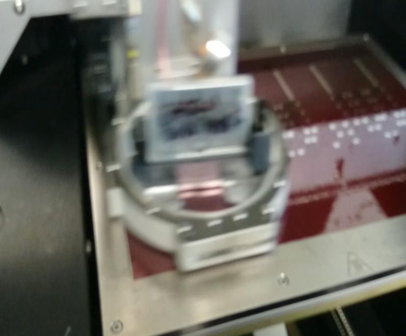
9 PEL 2014 Printed Electronics Ltd, Inkjet Systems for circuitry

10 Inkjet rapid prototyping Inkjet printed circuitry Manufactured in minutes SMT placement ~minutes to complete Using conductive epoxy (not solder) Pictured design Included Printed switch Printed Battery OLED Design to Manufactured Prototype Product in << one day. PEL 2013 Printed Electronics Ltd,

11 Pixdro LP50 Printing Etch Resist We design circuits Therefore we need various revisions of PCB design Although we are based in a PCB facility we often use the LP50 for ultra quick turn printed etch resist
")

12 Highest Potential Areas for P.E. Thinner Circuits Thin Circuits Large Area Thin substrates (as thin as 12um) have been printed successfully. Make use of both surfaces: print on 2 sizes of material Smart Integration Ultra Fine Features 3D Others PEL 2014 Printed Electronics Ltd,


13 Highest Potential Areas for P.E. Long & Large Area Electronics Very long (R2R) circuits Large Area Smart Integration Ultra Fine Features 3D Others Conventional Circuits are limited in size by manufacturing formats Using digital system one can print unlimited length Sensors, cable printing etc Can be reel-to-reel printed at km lengths e.g. CIT process ( CPI - PETEC


 PEL")

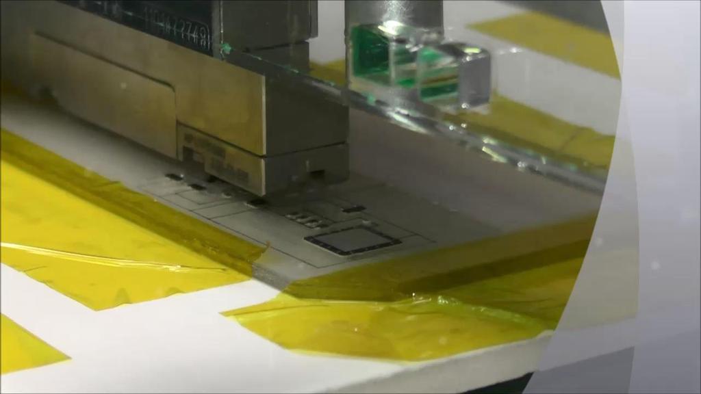
14 Interconnection and Fan Out Inkjet can be used for printing component fanouts (non contact method) PEL 2014 Printed Electronics Ltd,
 I will say now that printing an")
15 Device level interconnects e.g. Using digital printing to form chip-scale modules (or attachment) I will say now that printing an equivalent to wirebonds is very challenging so we focus here on other packaging areas.


16 Printing the interconnect onto the device Printed Ag lines are 50um in width Printed drop size is 1pl = ~50um Inkjet Nano Silver Ink PragmatIC transistor device PEL 2014 Printed Electronics Ltd,


17 So what is the downside to Inkjet? Printing acuity Accuracy Materials Drops are quite big (~50um) Viscosity and Surface Tension capillary action The ink is mostly solvent actually
18 Jet-printed Interconnects
")

 Low density & complexity High Yields Attach")

19 Highest Potential Areas for P.E. Integration Package to Flex Very long (R2R) circuits Large Area Smart Integration Ultra Fine Features 3D Others Use modular approach Print large low cost substrates (P.E.) Low density & complexity High Yields Attach small modules of high density circuitry for functionality Conventional electronics Uses Pick and Place with e.g. conductive epoxy

20 Hybrid Device Integration Printed EC Display Screen Printed & Inkjet Traces Dispenser conductive adhesive
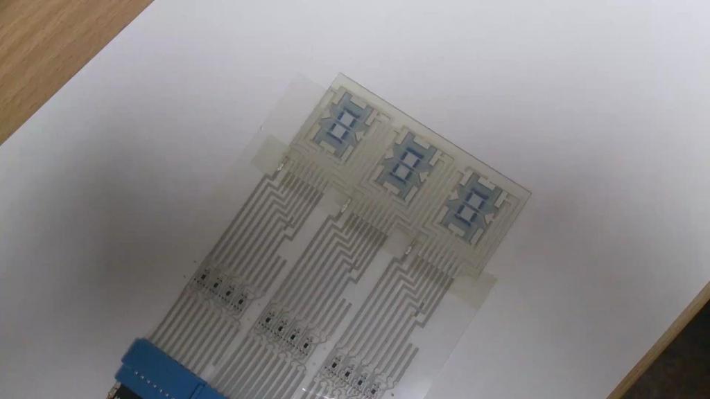
21 Interconnection - integration


22 Inkjet Scale vs Silicon scale Inkjet Scale um printed lines are usual in inkjet circuits. Silicon edge interconnection Connections to silicon are at micron scale 150um PEL 2014 Printed Electronics Ltd,


23 Super Ink Jet (SIJ) Key Points: Sub-femtolitre drop size Electrostatic drop ejection Line widths of 1um or less are possible PEL 2014 Printed Electronics Ltd,

24 SIJ Examples PEL 2014 Printed Electronics Ltd,

25 PEL 2014 Printed Electronics Ltd, Fanout features (~10um)


26 Real time view of printing Confidential On Si substrate, Silver Nanopaste, Line pitch 15mm Line pitch 15 mm light SIJ-head CCD PEL


 At room")
27 Confidential Vertical structures using super inkjet PEL Real time video In air atmosphere, (no chamber) At room temperature light SIJ-head CCD

, 2015 IEEE 65 th Date of Conference: 26-29 PEL May 20152015Page(s):41 Printed - 45 Electronics Ltd, www.")
28 TSV filling by Super Inkjet TSV structure: tapered vias with bottom diameter of 10μm, top diameter of 23 μm and depth of 36 μm. Research Level Work Top View Metallization of High Density TSVs using Super Inkjet Technology Behnam Khorramdel, Mika Matti Laurila, and Matti Mäntysalo Tampere University of Technology Department of Electronics and Communications Engineering Published in: Electronic Components and Technology Conference (ECTC), 2015 IEEE 65 th Date of Conference: PEL May Page(s):41 Printed - 45 Electronics Ltd,
29 3D interconnection


30 3D Inkjet System PEL-developed proof of concept inkjet printing system for curved surfaces. PEL System

31 Embedded electronics on a curved surface
32 Capability What capabilities can printing technology offer today? Digital (e.g. inkjet) is strong but inks are still imperfect. New printhead systems overcome many problems - but not all. Sometimes inkjet is not suitable (e.g. for finer features or thicker layers) In this case other techniques are essential (Screen, Aerosol Jet, SIJ etc) Lithography is still a big part of the picture. We need to work with hybrid interconnection
33 Reduce time to market How to combine technologies from a system integration perspective, to rapid prototype applications and allow quicker customer trials and shorter time-to-market? Needs a creative approach on all sides. E.g. We may need to persuade customers to accept a different type of interconnect from that which they are used to. New techniques will push this e.g. combination of 3D printing and additive circuit printing.
34 Thank you
MID Manufacturing Process.
 3D Aerosol Jet Printing An Emerging MID Manufacturing Process. Dr. Martin Hedges Neotech Services MTP, Nuremberg, Germany info@neotechservices.com Aerosol Jet Printing Aerosol Jet Process Overview Current
Inkjet Filling of TSVs with Silver Nanoparticle Ink. Behnam Khorramdel, Matti Mäntysalo Tampere University of Technology ESTC 2014 Finland, Helsinki
 Inkjet Filling of TSVs with Silver Nanoparticle Ink Behnam Khorramdel, Matti Mäntysalo Tampere University of Technology ESTC 2014 Finland, Helsinki Outline Motivation for this study Inkjet in MEMS fabrication
shaping global nanofuture ULTRA-PRECISE PRINTING OF NANOMATERIALS
 shaping global nanofuture ULTRA-PRECISE PRINTING OF NANOMATERIALS WHO ARE WE? XTPL S.A. is a company operating in the nanotechnology segment. The interdisciplinary team of XTPL develops on a global scale
Processes for Flexible Electronic Systems
 Processes for Flexible Electronic Systems Michael Feil Fraunhofer Institut feil@izm-m.fraunhofer.de Outline Introduction Single sheet versus reel-to-reel (R2R) Substrate materials R2R printing processes
Accelerating Scale Up of Large Area Electronics
 Accelerating Scale Up of Large Area Electronics Duncan Lindsay Business Development Director, CPI 2015 Centre for Process Innovation Limited. All Rights Reserved. Who are CPI? CPI is a UK technology innovation
Passive Direct Print Sensors
 Passive Wireless Sensor Technology Workshop June 6-7, 2012 Hyatt Regency, La Jolla, CA Passive Direct Print Sensors Mike Newton mnewton@nscrypt.com nscrypt Inc. Orlando, Florida University of Texas at
B. Flip-Chip Technology
 B. Flip-Chip Technology B1. Level 1. Introduction to Flip-Chip techniques B1.1 Why flip-chip? In the development of packaging of electronics the aim is to lower cost, increase the packaging density, improve
Properties. -Print & Printable Electronics. *Dr. Kazuhiro Murata, **Dr. Kazuyuki Masuda
 -Print & Printable Electronics esuper Inkjet Printer Technology and Its Properties *Dr. Kazuhiro Murata, **Dr. Kazuyuki Masuda *National Institute of Advanced Industrial Science and Technology, ** SIJ
National Centre for Flexible Electronics
 National Centre for Flexible Electronics Tripartite Partnership Government FlexE Centre - A platform for a meaningful interaction between industry and academia. An interdisciplinary team that advances
Figure 7 Dynamic range expansion of Shack- Hartmann sensor using a spatial-light modulator
 Figure 4 Advantage of having smaller focal spot on CCD with super-fine pixels: Larger focal point compromises the sensitivity, spatial resolution, and accuracy. Figure 1 Typical microlens array for Shack-Hartmann
Picoliter Solder Droplet Dispensing
 Picoliter Solder Droplet Dispensing Ronald E. Marusak, Ph.D. MicroFab Technologies, Inc. 1104 Summit, Suite 110 Plano, Texas 75074 (214) 578-8076 A device based on ink-jet printing technology was used
The Use of Inkjet Printing Technology for Fabricating Electronic Circuits The Promise and the Practical
 The Use of Inkjet Printing Technology for Fabricating Electronic Circuits The Promise and the Practical Brian Amos Engineering Manager, Dow Electronic Materials, Marlborough, MA, USA Thomas Sutter Emerging
POSSUM TM Die Design as a Low Cost 3D Packaging Alternative
 POSSUM TM Die Design as a Low Cost 3D Packaging Alternative The trend toward 3D system integration in a small form factor has accelerated even more with the introduction of smartphones and tablets. Integration
Aerosol Jet technology opportunities
 Aerosol Jet technology opportunities Jiří Navrátil 1. Introduction history and formation 2. Aerosol Jet system 2.1 System components 2.2 Inks and substrates 3. Application of Aerosol Jet technology 4.
Effect of Corona Treatment on Spreading Behavior of UV Ink over Inkjet Printed Silver Nano-Particle Layer
 Effect of Corona Treatment on Spreading Behavior of UV Ink over Inkjet Printed Silver Nano-Particle Layer Khushbeen Department of Printing Technology GJUS&T, Hisar, Haryana, India Email- khushveen12@gmail.com
Flexible Hybrid Electronics Fabricated with High-Performance COTS ICs using RTI CircuitFilm TM Technology
 Flexible Hybrid Electronics Fabricated with High-Performance COTS ICs using RTI CircuitFilm TM Technology Scott Goodwin 1, Erik Vick 2 and Dorota Temple 2 1 Micross Advanced Interconnect Technology Micross
Manufacture and Performance of a Z-interconnect HDI Circuit Card Abstract Introduction
 Manufacture and Performance of a Z-interconnect HDI Circuit Card Michael Rowlands, Rabindra Das, John Lauffer, Voya Markovich EI (Endicott Interconnect Technologies) 1093 Clark Street, Endicott, NY 13760
Fully Printed Conformal Antenna and Sensors on 3D Plastic, Ceramic, and Metallic Substrates. Mike O Reilly
 Fully Printed Conformal Antenna and Sensors on 3D Plastic, Ceramic, and Metallic Substrates Mike O Reilly imaps NE 2016 Antenna and sensor printing via Aerosol Jet Optomec has developed high volume 3D
Ricoh Industrial Ink Jet Technology
 Ricoh Industrial Ink Jet Technology Ink Jet Business Division EMEA IMI Barcelona, November 2014 Presentation Outline HISTORY & ORGANIZATION SOLUTIONS TECHNOLOGY Who is Ricoh? Founded in 1936 108,000+ Employees
Printed Electronics. Applications
 Printed Electronics Research Through University-Industry Partnerships Outline Background on Printed Electronics (PE) Corporate Partnerships Raytheon UMass Lowell Research Institute (RURI) Printed Electronics
VELOX IDS 250. Direct-to-shape digital decoration for mass production of cylindrical containers. Unprecedented decoration quality
 VELOX IDS 250 Direct-to-shape digital decoration for mass production of cylindrical containers Unprecedented decoration quality Total operational agility Low total cost of ownership DIGITAL PACKAGING DECORATION
The Future for Printed Electronics
 The Future for Printed Electronics Jon Helliwell National Centre for Printable Electronics 24 October, 2013 Copyright CPI 2013. All rights reserved What is Printed Electronics? Organic and printed electronics
Making a Material Difference
 Making a Material Difference Founded as a QinetiQ corporate investment in January 2002 Spun out in 2007 Locations: Rochester, NYS, USA (HQ and Production) Farnborough and Malvern, UK (R&D, Production and
450mm and Moore s Law Advanced Packaging Challenges and the Impact of 3D
 450mm and Moore s Law Advanced Packaging Challenges and the Impact of 3D Doug Anberg VP, Technical Marketing Ultratech SOKUDO Lithography Breakfast Forum July 10, 2013 Agenda Next Generation Technology
AEROSOL JET PRINTING SYSTEM FOR HIGH SPEED, NON-CONTACT FRONT SIDE METALLIZATION OF SILICON SOLAR CELLS
 AEROSOL JET PRINTING SYSTEM FOR HIGH SPEED, NON-CONTACT FRONT SIDE METALLIZATION OF SILICON SOLAR CELLS Bruce H. King and Stephen M. Barnes Optomec, Inc. 3911 Singer NE, Albuquerque, NM 87109, US Phone
Здра вствуйте, това рищи!
 Manufacturing of Smart Objects by Printing Technologies Здра вствуйте, това рищи! Moscow / RUS, June 05, 2013 Reinhard R. Baumann Chemnitz University of Technology Chair of Digital Printing Fraunhofer
EMERGING SUBSTRATE TECHNOLOGIES FOR PACKAGING
 EMERGING SUBSTRATE TECHNOLOGIES FOR PACKAGING Henry H. Utsunomiya Interconnection Technologies, Inc. Suwa City, Nagano Prefecture, Japan henryutsunomiya@mac.com ABSTRACT This presentation will outline
Technology Overview. Blind Micro-vias. Embedded Resistors. Chip-on-flex. Multi-Tier Boards. RF Product. Multi-chip Modules. Embedded Capacitance
 Blind Micro-vias Embedded Resistors Multi-Tier Boards Chip-on-flex RF Product Multi-chip Modules Embedded Capacitance Technology Overview Fine-line Technology Agenda Corporate Overview Company Profile
SiP packaging technology of intelligent sensor module. Tony li
 SiP packaging technology of intelligent sensor module Tony li 2016.9 Contents What we can do with sensors Sensor market trend Challenges of sensor packaging SiP technology to overcome challenges Overview
Printing versus coating technology Which way Printed Electronics with solution coating will go?
 Printing versus coating technology Which way Printed Electronics with solution coating will go? Frank Schäfer, Andrea Glawe, Dr. Daniel Eggerath, KROENERT GmbH& Co KG, Schuetzenstrasse 105, 22761 Hamburg
SOLDERABLE ANISOTROPIC CONDUCTIVE ADHESIVES FOR 3D PACKAGE APPLICATIONS
 SOLDERABLE ANISOTROPIC CONDUCTIVE ADHESIVES FOR 3D PACKAGE APPLICATIONS ABSTRACT: Dr. Mary Liu and Dr. Wusheng Yin YINCAE Advanced Materials, LLC Albany, NY 3D packaging has recently become very attractive
Industry trends are boosting Jet Printing. Nico Coenen Global Sales Director Jet Printing
 Industry trends are boosting Jet Printing Nico Coenen Global Sales Director Jet Printing Agenda What is Jet Printing Market Overview Industry Trends Typical Applications 2 What is Jet Printing What is
A Miniaturized Multi-Channel TR Module Design Based on Silicon Substrate
 Progress In Electromagnetics Research Letters, Vol. 74, 117 123, 2018 A Miniaturized Multi-Channel TR Module Design Based on Silicon Substrate Jun Zhou 1, 2, *, Jiapeng Yang 1, Donglei Zhao 1, and Dongsheng
Micro-PackS, Technology Platform. Security Characterization Lab Opening
 September, 30 th 2008 Micro-PackS, Technology Platform Security Characterization Lab Opening Members : Micro-PackS in SCS cluster From Silicium to innovative & commucating device R&D structure, gathering
Direct printing tools for flexible hybrid electronics assembly. David Grierson, Ph.D. President & CTO of systemech, LLC
 Direct printing tools for flexible hybrid electronics assembly David Grierson, Ph.D. President & CTO of systemech, LLC We solve the problem of placing ultra-thin, high-performance Si devices onto flexible
QUALITY SEMICONDUCTOR, INC.
 Q QUALITY SEMICONDUCTOR, INC. AN-20 Board Assembly Techniques for 0.4mm Pin Pitch Surface Mount Packages Application Note AN-20 The need for higher performance systems continues to push both silicon and
A Low-cost Through Via Interconnection for ISM WLP
 A Low-cost Through Via Interconnection for ISM WLP Jingli Yuan, Won-Kyu Jeung, Chang-Hyun Lim, Seung-Wook Park, Young-Do Kweon, Sung Yi To cite this version: Jingli Yuan, Won-Kyu Jeung, Chang-Hyun Lim,
Printable Electronics
 Printable Electronics Printable Electronics The Centre for Process Innovation From innovation to commercialisation The Centre for Process Innovation From innovation to commercialisation The High Value
Smart Devices of 2025
 Smart Devices of 2025 Challenges for Packaging of Future Device Technologies Steve Riches/Kevin Cannon Tribus-D Ltd CW Workshop 27 March 2018 E:mail: info@tribus-d.uk M: 07804 980 954 Assembly Technology
Advanced Packaging - Pulsed-laser Heating for Flip Chip Assembly
 Page 1 of 5 Pulsed-laser Heating for Flip Chip Assembly A stress-free alternative By Thorsten Teutsch, Ph.D., Pac Tech USA, Elke Zakel, Ph.D., and Ghassem Azdasht, Pac Tech GmbH As flip chip applications
Inkjet resist inks. Krishna Balantrapu
 Inkjet resist inks Krishna Balantrapu OUTLINE Conventional Vs. Inkjet-Cost Savings Inkjet Material Design Inkjet Equipment-Lunaris Future work 2 DOW-R&D DRIVERS FOR NEW PRODUCT DEVELOPMENT Technology Need
Fraunhofer IZM - ASSID
 FRAUNHOFER-INSTITUT FÜR Zuverlässigkeit und Mikrointegration IZM Fraunhofer IZM - ASSID All Silicon System Integration Dresden Heterogeneous 3D Wafer Level System Integration 3D system integration is one
MICROFLEX Project: MEMS on New Emerging Smart Textiles/Flexibles
 MICROFLEX Project: MEMS on New Emerging Smart Textiles/Flexibles S Beeby, M J Tudor, R Torah, K Yang, Y Wei Dr Steve Beeby ESD Research Group Smart Fabrics 2011 5 th April 2011 Overview Introduce the MicroFlex
Just where it s needed
 Seite/Page: 1 Just where it s needed Continuing miniaturisation of many products requires a method of dispensing very small amounts of liquids Inkjet technology is capable of applying adhesives and many
Innovations Push Package-on-Package Into New Markets. Flynn Carson. STATS ChipPAC Inc Kato Rd Fremont, CA 94538
 Innovations Push Package-on-Package Into New Markets by Flynn Carson STATS ChipPAC Inc. 47400 Kato Rd Fremont, CA 94538 Copyright 2010. Reprinted from Semiconductor International, April 2010. By choosing
FUJIFILM Dimatix Technology Integration:
 News Release Editorial Contact: Edward Chrusciel FUJIFILM Dimatix 603-443-5364 echrusciel@dimatix.com FOR IMMEDIATE RELEASE FUJIFILM Dimatix Technology Integration: Helping companies incorporate the power
Application Bulletin 240
 Application Bulletin 240 Design Consideration CUSTOM CAPABILITIES Standard PC board fabrication flexibility allows for various component orientations, mounting features, and interconnect schemes. The starting
The Future of Packaging ~ Advanced System Integration
 The Future of Packaging ~ Advanced System Integration Enabling a Microelectronic World R. Huemoeller SVP, Adv. Product / Platform Develop June 2013 Product Segments End Market % Share Summary 2 New Product
Printing Beyond Color. Printed Smart Objects on Advanced Paper Substrates. Reinhard R. Baumann
 Printing Beyond Color Printed Smart Objects on Advanced Paper Substrates June 17, 2009 member of Reinhard R. Baumann member of Chemnitz University of Technology Institute for Print and Media Technology
Lecture: Integration of silicon photonics with electronics. Prepared by Jean-Marc FEDELI CEA-LETI
 Lecture: Integration of silicon photonics with electronics Prepared by Jean-Marc FEDELI CEA-LETI Context The goal is to give optical functionalities to electronics integrated circuit (EIC) The objectives
MEMS in ECE at CMU. Gary K. Fedder
 MEMS in ECE at CMU Gary K. Fedder Department of Electrical and Computer Engineering and The Robotics Institute Carnegie Mellon University Pittsburgh, PA 15213-3890 fedder@ece.cmu.edu http://www.ece.cmu.edu/~mems
DIGITAL PACKAGING DECORATION
 DIGITAL PACKAGING DECORATION Direct-to-shape digital decoration for mass production of cylindrical containers Unprecedented decoration quality Total operational agility Low total cost of ownership DIGITAL
Through Glass Via (TGV) Technology for RF Applications
 Technology for RF Applications") Through Glass Via (TGV) Technology for RF Applications C. H. Yun 1, S. Kuramochi 2, and A. B. Shorey 3 1 Qualcomm Technologies, Inc. 5775 Morehouse Dr., San Diego, California 92121, USA Ph: +1-858-651-5449,
Through Glass Via (TGV) Technology for RF Applications C. H. Yun 1, S. Kuramochi 2, and A. B. Shorey 3 1 Qualcomm Technologies, Inc. 5775 Morehouse Dr., San Diego, California 92121, USA Ph: +1-858-651-5449,
AEROSOL JET PRINTING OF CONDUCTIVE EPOXY FOR 3D PACKAGING
 AEROSOL JET PRINTING OF CONDUCTIVE EPOXY FOR 3D PACKAGING Michael J. Renn, Ph.D., and Kurt K. Christenson, Ph.D. Optomec, Inc. St. Paul, MN, USA mrenn@optomec.com and kchristenson@optomec.com Donald Giroux
Silicon Interposers enable high performance capacitors
 Interposers between ICs and package substrates that contain thin film capacitors have been used previously in order to improve circuit performance. However, with the interconnect inductance due to wire
Application Note AN-1011
 AN-1011 Board Mounting Application Note for 0.800mm Pitch Devices For part numbers IRF6100, IRF6100PBF, IR130CSP, IR130CSPPBF, IR140CSP, IR140CSPPBF, IR1H40CSP, IR1H40CSPPBF By Hazel Schofield and Philip
Technology Behind the Digital Magic
 Technology Behind the Digital Magic A Crash Course on Industrial Printing John Sweeterman General Manager Digital Division INX International Ink Co Deliver a Unique Experience for Everyone Why make the
Electrohydrodynamic Direct-Writing for Flexible Electronic Manufacturing
 Electrohydrodynamic Direct-Writing for Flexible Electronic Manufacturing Zhouping Yin YongAn Huang Yongqing Duan Haitao Zhang Electrohydrodynamic Direct-Writing for Flexible Electronic Manufacturing 123
Fully printable, strain-engineered electronic wrap for
 Supplementary Information Fully printable, strain-engineered electronic wrap for customizable soft electronics Junghwan Byun, Byeongmoon Lee, Eunho Oh, Hyunjong Kim, Sangwoo Km, Seunghwan Lee, and Yongtaek
Issues and Approaches Imposed on Ink Jet Technologies for the Progress of Printed Electronics
 Fujii: Issues and Approaches Imposed on Ink-Jet Technologies (1/5) [Technical Paper] Issues and Approaches Imposed on Ink Jet Technologies for the Progress of Printed Electronics Masahiko Fujii Ink jet
RIT. Printing. Project Goals. Printing Radio Frequency Identification (RFID) Tag Antennas Using Inks Containing Metal Nanoparticles
 Tag Antennas Using Inks Containing Metal Nanoparticles") Printing Radio Frequency Identification (RFID) Tag Antennas Using Inks Containing Metal Nanoparticles Bruce E. Kahn Rochester Institute of Technology bkahn@mail.rit.edu http://www.rit.edu/~bekpph/ RIT
Printing Radio Frequency Identification (RFID) Tag Antennas Using Inks Containing Metal Nanoparticles Bruce E. Kahn Rochester Institute of Technology bkahn@mail.rit.edu http://www.rit.edu/~bekpph/ RIT
New fabrication and packaging technologies for CMOS pixel sensors: closing gap between hybrid and monolithic
 New fabrication and packaging technologies for CMOS pixel sensors: closing gap between hybrid and monolithic Outline Short history of MAPS development at IPHC Results from TowerJazz CIS test sensor Ultra-thin
Simulation of High Resistivity (CMOS) Pixels
 Pixels") Simulation of High Resistivity (CMOS) Pixels Stefan Lauxtermann, Kadri Vural Sensor Creations Inc. AIDA-2020 CMOS Simulation Workshop May 13 th 2016 OUTLINE 1. Definition of High Resistivity Pixel Also
Simulation of High Resistivity (CMOS) Pixels Stefan Lauxtermann, Kadri Vural Sensor Creations Inc. AIDA-2020 CMOS Simulation Workshop May 13 th 2016 OUTLINE 1. Definition of High Resistivity Pixel Also
Organic Packaging Substrate Workshop Overview
 Organic Packaging Substrate Workshop Overview Organized by: International Electronics Manufacturing Initiative (inemi) Mario A. Bolanos November 17-18, 2009 1 Organic Packaging Substrate Workshop Work
mcube WLCSP Application Note
 AN-002 Rev.02 mcube WLCSP Application Note AN-002 Rev.02 mcube, Inc. 1 / 20 AN-002 Rev.02 Guidelines for Printed Circuit Board (PCB) Design and Assembly with mcube Wafer Level Chip Scale Package (WLCSP)
Flip chip Assembly with Sub-micron 3D Re-alignment via Solder Surface Tension
 Flip chip Assembly with Sub-micron 3D Re-alignment via Solder Surface Tension Jae-Woong Nah*, Yves Martin, Swetha Kamlapurkar, Sebastian Engelmann, Robert L. Bruce, and Tymon Barwicz IBM T. J. Watson Research
Printable, Novel CNT Inks with V2V Technology
 Printable, Novel CNT Inks with V2V Technology William J. Hurley, Jr., PhD Chasm Technologies, Inc. Canton, MA June 23, 2010 New England Nanomanufacturing Summit 1 Outline CHASM Overview Alliance with SWeNT
APPLICATION NOTE 6381 ORGANIC LAND GRID ARRAY (OLGA) AND ITS APPLICATIONS
 AND ITS APPLICATIONS") Keywords: OLGA, SMT, PCB design APPLICATION NOTE 6381 ORGANIC LAND GRID ARRAY (OLGA) AND ITS APPLICATIONS Abstract: This application note discusses Maxim Integrated s OLGA and provides the PCB design and
Keywords: OLGA, SMT, PCB design APPLICATION NOTE 6381 ORGANIC LAND GRID ARRAY (OLGA) AND ITS APPLICATIONS Abstract: This application note discusses Maxim Integrated s OLGA and provides the PCB design and
Image Sensor Advanced Package Solution. Prepared by : JL Huang & KingPak RD division
 Image Sensor Advanced Package Solution Prepared by : JL Huang & KingPak RD division Contents CMOS image sensor marketing overview Comparison between different type of CMOS image sensor package Overview
Inkjet Printing of Biomedical Adhesives
 Mater. Res. Soc. Symp. Proc. Vol. 95 27 Materials Research Society 95-D12-5 Inkjet Printing of Biomedical Adhesives Anand Doraiswamy 1, Jan Sumerel 2, Jonathan Wilker 3, and Roger J Narayan 1 1 University
Min Tao, Ph. D, Ashok Prabhu, Akash Agrawal, Ilyas Mohammed, Ph. D, Bel Haba, Ph. D Oct , IWLPC
 PACKAGE-ON-PACKAGE INTERCONNECT FOR FAN-OUT WAFER LEVEL PACKAGES Min Tao, Ph. D, Ashok Prabhu, Akash Agrawal, Ilyas Mohammed, Ph. D, Bel Haba, Ph. D Oct 18-20 2016, IWLPC 1 Outline Laminate to Fan-Out
Overcoming the Challenges of HDI Design
 ALTIUMLIVE 2018: Overcoming the Challenges of HDI Design Susy Webb Design Science Sr PCB Designer San Diego Oct, 2018 1 Challenges HDI Challenges Building the uvia structures The cost of HDI (types) boards
Additive & Inkjet Printing Technologies & Applications
 Additive & Inkjet Printing Technologies & Applications Debbie Thorp, Business Development Director Global Inkjet Systems Ltd Silverstone Park - October 2018 GIS Products DFE Atlas User Interface Machine
PCB Supplier of the Best Quality, Lowest Price and Reliable Lead Time. Low Cost Prototype Standard Prototype & Production Stencil PCB Design
 The Best Quality PCB Supplier PCB Supplier of the Best Quality, Lowest Price Low Cost Prototype Standard Prototype & Production Stencil PCB Design Visit us: www. qualiecocircuits.co.nz OVERVIEW A thin
Printing Processes and their Potential for RFID Printing
 Printing Processes and their Potential for RFID Printing Anne Blayo and Bernard Pineaux, EFPG 1 - Printing processes - A.Blayo and B. Pineaux - soc -EUSAI - 12th October 2005, Grenoble Outline General
SPECIFICATION FOR APPROVAL 1/8W 0816 LOW RESISTNACE CHIP RESISTOR
 PAGE : 1 OF 11 1/8W 0816 LOW RESISTNACE CHIP RESISTOR 1. Scope This specification applies to 0.8mm x 1.60mm size 1/8W, fixed metal film chip resistors rectangular type for use in electronic equipment.
High Reliability and High Temperature Application Solution Solder Joint Encapsulant Paste
 High Reliability and High Temperature Application Solution Solder Joint Encapsulant Paste YINCAE Advanced Materials, LLC WHITE PAPER October 2017 2017 YINCAE Advanced Materials, LLC - All Rights Reserved.
License to Speed: Extreme Bandwidth Packaging
 License to Speed: Extreme Bandwidth Packaging Sean S. Cahill VP, Technology BridgeWave Communications Santa Clara, California, USA BridgeWave Communications Specializing in 60-90 GHz Providing a wireless
Brief Introduction of Sigurd IC package Assembly
 Brief Introduction of Sigurd IC package Assembly Content Package Development Trend Product Brief Sawing type QFN Representative MEMS Product LGA Light Sensor Proximity Sensor High Yield Capability Low
Intel's 65 nm Logic Technology Demonstrated on 0.57 µm 2 SRAM Cells
 Intel's 65 nm Logic Technology Demonstrated on 0.57 µm 2 SRAM Cells Mark Bohr Intel Senior Fellow Director of Process Architecture & Integration Intel 1 What are We Announcing? Intel has fabricated fully-functional
EMERGING INKJET PRINTING TECHNOLOGIES, APPLICATIONS AND GLOBAL MARKETS
 EMERGING INKJET PRINTING TECHNOLOGIES, APPLICATIONS AND GLOBAL MARKETS AVM091B November 2014 Andrew McWilliams Project Analyst ISBN: 1-56965-999-0 BCC Research 49 Walnut Park, Building 2 Wellesley, MA
Bumping of Silicon Wafers using Enclosed Printhead
 Bumping of Silicon Wafers using Enclosed Printhead By James H. Adriance Universal Instruments Corp. SMT Laboratory By Mark A. Whitmore DEK Screen Printers Advanced Technologies Introduction The technology
Modeling, Design, and Demonstration of 2.5D Glass Interposers for 16-Channel 28 Gbps Signaling Applications
 Modeling, Design, and Demonstration of 2.5D Glass Interposers for 16-Channel 28 Gbps Signaling Applications Brett Sawyer, Bruce C. Chou, Saumya Gandhi, Jack Mateosky, Venky Sundaram, and Rao Tummala 3D
Printed Electronics and Additive Microelectronic Packaging For RF/Microwave Applications
 Printed Electronics and Additive Microelectronic Packaging For RF/Microwave Applications Prof. Craig Armiento University of Massachusetts Lowell Raytheon UMass Lowell Research Institute (RURI) Printed
Recent Developments in Multifunctional Integration. Stephan Guttowski, Head of Technology Park»Heterointegration«, Fraunhofer FMD
 Recent Developments in Multifunctional Integration Stephan Guttowski, Head of Technology Park»Heterointegration«, Fraunhofer FMD Founding Participants 2 One-Stop-Shop for developments from wafer technologies
PRESS KIT. High Accuracy Device Bonder with Robotics.
 PRESS KIT High Accuracy Device Bonder with Robotics Press Announcement SET Introduces FC300R High Accuracy Device Bonder with Robotics FC300R: an Easy-to-Use Production Platform Ideal for High Accuracy
Heterogeneous integration of autonomous smart films based on electrochromic transistors
 of autonomous smart films NEWSLETTER #5 www.smartwww.smart-ec.eu Objectives SMART-EC has finalized last August 2014; it aimed at the development of self-powered electrochromic (EC) display device with
Wirelessly powered micro-tracer enabled by miniaturized antenna and microfluidic channel
 Journal of Physics: Conference Series PAPER OPEN ACCESS Wirelessly powered micro-tracer enabled by miniaturized antenna and microfluidic channel To cite this article: G Duan et al 2015 J. Phys.: Conf.
Electroless Bumping for 300mm Wafers
 Electroless Bumping for 300mm Wafers T. Oppert Internepcon 2006 Tokyo Big Sight, Japan Outline Short Company Profile Electroless Ni/Au Under Bump Metallization UBM for Copper Devices Solder Bumping: Stencil
The Impact of Reduced Solder Alloy Powder Size on Solder Paste Print Performance. Presented by Karl Seelig, V.P. Technology AIM Metals & Alloys
 The Impact of Reduced Solder Alloy Powder Size on Solder Paste Print Performance Presented by Karl Seelig, V.P. Technology AIM Metals & Alloys Solder Powder Solder Powder Manufacturing and Classification
BGA (Ball Grid Array)
") BGA (Ball Grid Array) National Semiconductor Application Note 1126 November 2002 Table of Contents Introduction... 2 Package Overview... 3 PBGA (PLASTIC BGA) CONSTRUCTION... 3 TE-PBGA (THERMALLY ENHANCED
BGA (Ball Grid Array) National Semiconductor Application Note 1126 November 2002 Table of Contents Introduction... 2 Package Overview... 3 PBGA (PLASTIC BGA) CONSTRUCTION... 3 TE-PBGA (THERMALLY ENHANCED
Thin Film Resistor Integration into Flex-Boards
 Thin Film Resistor Integration into Flex-Boards 7 rd International Workshop Flexible Electronic Systems November 29, 2006, Munich by Dr. Hans Burkard Hightec H MC AG, Lenzburg, Switzerland 1 Content HiCoFlex:
2015, ATLANTA - SGIA PRINTED ELECTRONICS SYMPOSIUM November 3rd 4th
 2015, ATLANTA - SGIA PRINTED ELECTRONICS SYMPOSIUM November 3rd 4th The Sperior Screenprinting Performance with Ultra-Hard Stainless Mesh -Strikingly Improved Dimension Accuracy- Advanced Screen Printing
IMAGING SILICON NANOWIRES
 Project report IMAGING SILICON NANOWIRES PHY564 Submitted by: 1 Abstract: Silicon nanowires can be easily integrated with conventional electronics. Silicon nanowires can be prepared with single-crystal
Laser Solder Attach for Optoelectronics Packages
 1 Laser Solder Attach for Optoelectronics Packages Elke Zakel, Lars Titerle, Thomas Oppert, Ronald G. Blankenhorn* Pac Tech Packaging Technologies GmbH Am Schlangenhorst 15-17, Germany Phone:+ 49 (0) 33
Precise Solder Dispensing In High-Throughput Microdevice Packaging Applications
 Precise Solder Dispensing In High-Throughput Microdevice Packaging Applications A high-precision, highthroughput solder paste dispensing process fills the gap between novel packaging design, traditional
Figure 7. Hot Carrier Damage Tracks the P-well Current.
 Hot Carrier Degradation Physics By Christopher Henderson One useful technique to indirectly observe the damage created by hot carriers is to measure the p-well current. The p-well current closely tracks
Fabricating 2.5D, 3D, 5.5D Devices
 Fabricating 2.5D, 3D, 5.5D Devices Bob Patti, CTO rpatti@tezzaron.com Tezzar on Semiconduct or 04/15/2013 1 Gen4 Dis-Integrated 3D Memory DRAM layers 42nm node 2 million vertical connections per lay per
5G Systems and Packaging Opportunities
 5G Systems and Packaging Opportunities Rick Sturdivant, Ph.D. Founder and Chief Technology Officer MPT, Inc. (www.mptcorp.com), ricksturdivant@gmail.com Abstract 5G systems are being developed to meet
FLEXIBLE HYBRID ELECTRONICS FOR ADDITIVE MANUFACTURING
 FLEXIBLE HYBRID ELECTRONICS FOR ADDITIVE MANUFACTURING JASON MARSH NEXTFLEX CTO JUNE 13 2017 WHAT IS NEXTFLEX? 6/13/2017 PAGE 1 PART OF A NETWORK OF MANUFACTURING INSTITUTES Across the Manufacturing USA