Printable Electronics
|
|
|
- Harold Gallagher
- 5 years ago
- Views:
Transcription

1 Printable Electronics Printable Electronics The Centre for Process Innovation From innovation to commercialisation
2 The Centre for Process Innovation From innovation to commercialisation The High Value Manufacturing Catapult is a partnership between industry and government, which is a catalyst for the future growth and success of manufacturing in the UK. Its long-term goal is to stimulate growth in the manufacturing sector and grow the sector s contribution to UK GDP to a level more commensurate with that of competitor economies. It does this by helping businesses accelerate new concepts (often started in research institutions) to commercial reality (where they can be funded through market sources). In doing so, the Catapult reduces companies risk in innovation, and it enables the UK to address market needs in key areas, making the country more competitive on the global stage. The High Value Manufacturing Catapult combines the strengths of seven UK technology and innovation centres, each focusing on major underpinning manufacturing technologies. The Catapult brings these centres together to develop cross sector manufacturing capabilities, which can span from raw materials to finished processes. It also enables innovation to cut across sectors by bringing together businesses from diverse industries and giving them access to a pool of world-class expertise, equipment and processes invested and supported by UK government. The Centre for Process Innovation is the UK s national technology and innovation centre to serve and support the process manufacturing industries. We are chosen by key industry leaders and SMEs to develop, prove, prototype and scale up the next generation of products and processes. We work across a range of technology platforms, each of which have the potential to generate a substantial impact on the future of manufacturing. We provide product and process development facilities and expertise in industrial biotechnology and biorefining, formulation and flexible manufacturing, printable electronics and biologics with the overall aim of creating less waste, cleaner, more efficient and more economic products and processes. Our open innovation model enables our clients to develop products and prove processes with minimal risk. We provide assets and expertise so our customers can demonstrate the process and prove it is feasible before investing substantial amounts of money in capital equipment and training. New products and processes can be proven; on paper, in the lab and in the plant before being manufactured at an industrial scale. By utilising our proven assets and expertise companies can take their products and processes to market faster. There is no down time in production as all of the process development is completed off-line. Better Products, Faster We help our clients to produce better products with increased quality and performance. We can create processes with higher yields and reduced manufacturing time with faster conversion of raw materials or feedstock to product. Low Cost, Low Waste Manufacturing We enable companies to decrease capital and manufacturing costs by facilitating batch to continuous processes, increased automation and reduced manufacturing time. We help reduce and reuse wastes, utilise natural materials and decrease reliance on fossil fuels.


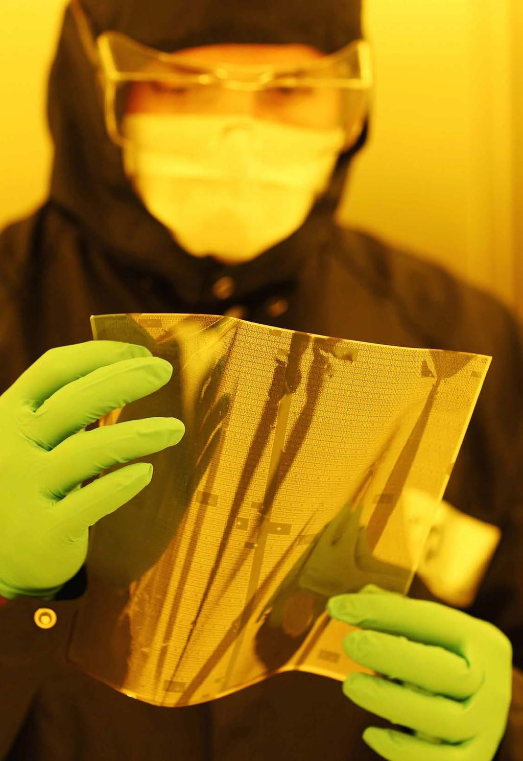
3 Introduction Printable Electronics at CPI CPI offers world class, open access capability for the scale up and commercialisation of new, innovative printed electronic products and applications. Our facilities and expertise provide clients with the environment to understand how their products and processes perform under manufacturing conditions and accelerate their commercial realisation. CPI focuses on the integration and manufacture of new innovative electronic devices, developing the technologies that will drive the manufacturing process forward. These new processes, including the printing of electronic functionality, open up a host of design opportunities and will lead to the creation of a range of future electronic applications in key market sectors such as print and packaging, healthcare, built environment, automotive and aerospace. The integration of electronics with flexible form factors increases the freedom for product designers to embed technology and functionality into their designs, creating the opportunity for new, innovative components that are wireless, smarter, interactive, conformable, thinner, lightweight, rugged and able to blend into the surrounding environment. These new ways of manufacturing electronics will give rise to a wide range of new, novel applications such as flexible displays for mobile devices, smart therapeutic bandages for managing and monitoring recovery of wounds, wearable electronics for monitoring and improving performance, wireless medical devices for rapid diagnostics using printed sensors, conformable lighting and intelligent packaging for consumer goods and industrial products, to name but a few. CPI is also working with its extensive networks of partners to develop new techniques and processes that will overcome some of the innovation challenges in printable electronics, such as the need for low cost ultra high performance barrier materials. Our facilities include: Inkjet Flex ; roll to roll inkjet printing of copper-based flexible circuits A specialist roll to roll line for the printing, coating and patterning of a range of organic and inorganic solution-based coatings 1250m 2 of class 1000 (ISO 6) and class 100 (ISO 5) cleanrooms and associated laboratory space 300mm wide roll to roll wet coat prototyping and processing in a class 1000 cleanroom Full lithography and subtractive patterning suite (eg. plasma etch) Additive pattern printing equipment inc. Litrex and Dimatix ink jets and Optomec aerosol jet Fully equipped materials preparation and formulation laboratory with characterisation instrumentation for rheometry, thermal (DSC, TGA) properties, FTIR, and surface energy Batch and roll to roll Atomic Layer Deposition for high-integrity conformal coatings Batch and continuous sputter coating in a class 1000 cleanroom environment An Integrated Smart Systems line capable of performing flexo, gravure, offset litho and rotary screen printing Large scale process development toolsets based on robotic handling with cassette to cassette-based transfers including: Large-area high-resolution coating for OSSL and PV applications Industry compatible coat-bake-develop and dry or wet-etch cluster tools In line sputter coating UV stepper exposure tool CD and overlay measurement Comprehensive measurement and characterisation equipment collated via customised informatics software


4 Our Services What we offer Incubation Support for SMEs Comprehensive facilities and scale-up expertise With a range of cost effective services, the highly skilled team at CPI can help to guide you from concept to finished product. In the development of new electronic products and processes, our experienced scientists, engineers, scale up experts, process operators and commercialisation specialists are able to take projects from early concepts through to innovative products. CPI has a significant track record in working with SMEs to help them move through the innovation phase in turning their research ideas into commercial applications that utilise printed electronics. CPI helps SMEs to identify and overcome their innovation challenges by providing technical expertise coupled with development and scale up facilities. We can help companies to understand the feasibility of their new product or process in a phased way that reduces risk for both the company and their investors. Some of the companies currently incubating at our National Printable Electronics Centre include: NeuDrive - flexible OTFT materials provider Polar OLED - flexible device supplier PolyPhotonix - healthcare PragmatIC - flexible IC Silent Sensors - device manufacturer SmartKem - semiconductors for flexible OLED displays Prototyping, Demonstration and Scale Up Materials Investigation Business and Funding Support Product and Process Development Consultancy Incubator Space POLYPHOTONIX


5 Optoelectronics Our Technologies Areas of expertise Thin Film Transistors and Sensors CPI has brought together sophisticated equipment alongside industry experts in key technology areas related to printable electronics, including: Optoelectronics Thin Film Transistors and Sensors Integrated Smart Systems Barrier and Vacuum Encapsulation Integrated Smart Systems Barrier and Vacuum Encapsulation
, organic photovoltaic (OPV) and light emitting electrochemical cell applications.")
 and roll to roll operations at pilot production scale.")
6 Opto Electronics OLED, organic photovoltaic and light emitting, electrochemical technologies CPI has extensive capability to support the development, scale-up and characterisation of organic light emitting diode (OLED), organic photovoltaic (OPV) and light emitting electrochemical cell applications. Offering a versatile equipment set, CPI allows customers to scale up their products and processes supporting feasibility proof of concept at small scale (100mm), sheet-to-sheet operations at GEN 2 (370x470mm) and roll to roll operations at pilot production scale. Proof of Concept CPI provides small scale ( mm substrate size) glove boxes with spin coating / evaporation technology that supports material and device design feasibilty studies. These systems focus on quick turnaround, proof of concept studies where the onus is on understanding the material and electrical characteristics, thereby aiding development of the device structure by speeding up process development and aid troubleshooting. The systems are typically manually loaded by the operator and are situated in a Class 1000 clean room environment. Pilot Production In order to scale up an optimised material set or device design, CPI offers an OLED/OPV prototyping line situated in a Class 100 clean room environment. Here the emphasis is on ensuring optimised manufacturing protocols. Substrates are transferred within dedicated processing cassettes with manual intervention kept to a minimum. Minimising defectivity within an OLED/OPV structure is a pre-requisite in guaranteeing device yield as the technology scales up to larger substrate sizes. A typical lighting structure can consist of 8-10 layers with layer thicknesses of < 50nm. CPI s pilot prouction scale system is dedicated to processing both air sensitive and non air sensitive material sets for the production of devices on substrates up to 200mm 2. The tool can accommodate the processing of both small molecule and solution based polymer materials and includes both slot die and spin coating techniques. Evaporation technology provides both inorganic cathode and organic small molecule capability. Device performance and lifetime are enhanced by the use of a dedicated encapsulation module to apply getters and adhesives. Fully automated robotic control, cassette to cassette handling and HEPA filtered laminar flow modules provide a unique environment to support high yield, low defect device production. The high resolution wide area line also has the ability to handle substrates of size 8 inch, 12 inch and GEN 2 scale (370mm x 470mm) The pilot line features sputter, dry etch, wet etch and cleaning capability and provides the ability to produce high quality lighting devices at pilotproduction scale. Roll to Roll Production CPI also provides further scale up capability in the form of a 300mm web roll to roll coater for the printing of a range of organic material sets. The system comprises of both slot die and screen printing capabilities, with options to upgrade to 500mm web width and to incorporate other printing techniques such as reverse gravure. The roll to roll machine houses a complementary encapsulation module, configured to allow the organic devices manufactured within the coater to be laminated with a barrier film. The tool provides protection to the device from water and oxygen ingress, both of which are known to be detrimental to device performance and lifetime.


7 Thin Film Transistors and Sensors Driving flexible electronic devices CPI has significant experience of working with clients to formulate a wide range of functional inks for printable electronics applications including sensors and organic thin film transistors; and using electronic materials, from graphene and carbon nanotubes to bio-materials and organic semiconductors. Working with CPI, companies can develop and characterise new ink formulations applicable for a number of printing techniques such as inkjet and aerosol jet, gravure, flexographic, offset lithographic and screen. We combine expertise in chemistry and device physics with advanced processing knowledge to produce optimal performance and stability from organic electronic device applications. CPI can also help to develop inks suitable for slot die and spin coating allowing companies to quickly scale up and integrate their new inks into a range of electronic products. Our facility is conveniently collocated with CPI s National Formulation and Graphene Application Centres, bringing together a multi-partner network that spans key knowledge partners and SME innovation enablers and providing industrytrained experts and open-access facilities to companies to develop and scale up advanced formulated products. By utilising our underpinning dispersion technologies, CPI provides the capability and experience to help companies to produce stable formulations that are suitable to scale up from the lab and into printed electronics based applications at pilot production scale. In addition, we can also help companies to select and optimise solvent systems, surfactants and resins. CPI can offer: Evaluation and development of inks for printed electronics applications Materials formulation development High resolution patterning and process development for displays Device design expertise Analytical capability Incubator space


8 Integrated Smart Systems Combining the benefits of conventional and printable electronics Above: Inkjet Flex, flexible copper circuit printing at CPI The Internet of Things promises to be one of the most revolutionary transformations in technology since the emergence of the Internet, with predictions indicating that more than 50 billion devices will be connected by Rapid Prototyping of Flexible Copper Circuits with Inkjet Flex CPI can offer: The commercialisation of associated applications requires devices which combine sensing, energy source, processing power and communications with a thin, flexible form factor. This is best achieved by integrated smart systems; adopting a hybrid approach where the processing power of conventional electronics is combined with the form factor and cost benefits of printable electronics. The manufacture of such devices requires a mix of capability such as placement techniques; adhesion, connectivity and encapsulation, all of which are housed at CPI. CPI s open access facilities and knowledge allows clients to test, develop and scale up a range of intelligent devices including smart labels, intelligent ticketing, printed switching, printed sensing, smart packaging and also wireless based applications such as Radio Frequency Identification (RFID) and Near- Field Communication (NFC). Working with CPI companies can develop their specific applications from initial device design, right through to the pilot production volumes needed for market testing and investment purposes. CPI s capability includes a high speed R2R electronics integration tool based on a Mühlbauer TAL to enable the manufacture of thin, flexible sensing systems for applications relevant to the Internet of Things. The tool integrates thin film and conventional electronics (packaged or bare die) onto circuits printed on reels of polymer film or paper up to 350mm wide. CPI also provides access to inkjet, flexo, gravure, offset litho and rotary screen printing processes. CPI s Inkjet Flex is a revolutionary two-stage print and plate process that enables copper to be printed onto PET substrates. The technology is applicable for a range of applications including printed antennae, sensors, electrodes, flexible pcbs and other components suitable for machine to machine communication devices. The Inkjet Flex capability allows clients to upload their copper based circuit designs and rapidly turn these designs into printed prototypes for initial feasibility and new product development work. Inkjet Flex is capable of producing copper features on flexible PET film using a continuous roll to roll printing and plating process. Samples are costed by the metre and can be produced on both clear and opaque substrates. Prototyping, demonstration and scale-up of RFID, NFC, smart packaging, labelling and machine to machine communication devices Testing, validation and optimisation of speciality inks: surface roughness, conductivity, scratch resistance, adhesion, sintering and high magnification microscopy Substrate evaluation Formulations and analytical capability Incubator space
, roll to roll sputtering and also a range of other sputtering and")

9 Barrier and Vacuum Encapsulation High performance large area coatings and processes CPI has extensive experience in the deposition and characterisation of barrier layers. We offer access to a wide variety of thin-film deposition systems including batch and roll to roll atomic layer deposition (ALD), roll to roll sputtering and also a range of other sputtering and vacuum coating technologies. CPI is engaged in a wide range of projects initially focussing on thin-film barrier technology for long-lasting and efficient flexible electronic devices. Further developments, up to pilot scale, are targeted in printable electronics applications in the display, photovoltaics, lighting and sensor fields with both rigid and flexible substrates utilising batch and processing techniques. CPI s equipment includes: Roll to roll atomic layer deposition Batch atomic layer deposition Pilot scale roll to roll sputtering In-line and batch sputtering In-line HiTUS sputtering coater (low ion energy bombardment during film growth) Analysis, characterisation and metrology CPI can offer: Access to a wide variety of thin-film deposition systems Industry experts in a wide range of vacuum processing and deposition technologies Expertise in combining vacuum coatings with more conventional coating technologies Expertise in a wide range of applications, including barrier and other coatings for application in printed electronics, optical, photovoltaic and other applications Access to a network of coating support and analytical capabilities, including barrier permeation characterisation


10 Our Markets CPI s expertise in printable electronics can be applied to a range of market applications, which have the potential for significant impact on the future of manufacturing in the UK. CPI focuses on the integration and manufacturing of new innovative electronic devices, developing the technologies that will drive the manufacturing process forward. The printing of electronic Automotive and Transport Aerospace Print and Packaging Healthcare functionality opens up a host of design opportunities and will lead to the creation of a range of future electronic applications in key market sectors. Household Goods Food and Drink Personal Care Automotive and Transport With the potential for improved control and operation through printed sensors, conformable integrated displays and lighting, printable electronics will provide users with a new and improved driving experience alongside improvements in the manufacturing process. CPI is working on bringing the following applications to the automotive market: Intelligent sensing Flexible, lightweight display screens Printed lighting Flexible solar technologies Head-up displays Aerospace CPI is focused on the commercialisation of new innovative technologies for the aviation sector. We offer product and process development capability in application areas such as: Intelligent sensing The Internet of Things Flexible, lightweight display screens Printed lighting Flexible solar technologies Head-up displays Built Environment Energy and Environment Materials Pharmaceuticals Electronics and IT Retail and Consumer Goods

 technologies, including: Due to its design freedom, printed electronics provide the opportunity to incorporate")


11 Print and Packaging Healthcare Household Goods Food and Drink CPI is working on the commercialisation of smart packaging and the Internet of Things for the print and packaging sector. Printable electronics is adding value to print through its convergence with the internet and its ease of integration with Near-Field Communication (NFC) and Radio Frequency Identification (RFID) technologies, including: Due to its design freedom, printed electronics provide the opportunity to incorporate electronic functionality into a wide range of medical and healthcare products. The technology encompasses thin, flexible, conformable and lightweight electronics opening up a range of opportunities for the sector including: Smart packaging CPI is working on the commercialisation of the following applications for the household goods market: Smart packaging and the Internet of Things Printed sensors in manufacturing and logistics tracking CPI is working on the new product development of the following for the food and drink industry: Sensors in manufacturing Packaging compliance Intelligence in logistics Smart packaging Smart labelling Anti-counterfeiting Track and trace Non-invasive screening Light therapies Healthcare photonics Printed sensing Product monitoring


12 Personal Care Built Environment Energy and the Environment Materials CPI is focused on the commercialisation of new innovative technologies for the personal care industry. We offer product and process development capability in application areas such as: Sensors in manufacturing Intelligence in packaging Intelligence in logistics CPI is focused on the commercialisation of new innovative technologies for the built environment. We offer product and process development capability in application areas such as: Flexible, lightweight display screens Printed lighting Flexible solar technologies Intelligent sensing CPI provides specialist expertise in new product development for printed solar technologies such as PV, OPV and BIPV. Innovations in solar technology will facilitate new designs for solar panels with thin, lightweight encapsulating envelopes and flexible form factors. The technology will make solar panels suitable for applications where flexibility, product shape and aesthetic value are important. Flexible photovoltaic technology will allow designers to apply and integrate solar energy into a wide range of surfaces within the built environment such as building roofs, walls, windows, lightings and fabric applications. CPI provides specialist expertise in the new product development of printed sensing capability for applications in the materials and chemicals industry. We can work with you to develop innovations in: Printed sensors in manufacturing Intelligence in logistics


13 Pharmaceuticals Electronics and IT Retail and Consumer Goods CPI provides specialist expertise in the new product development of printed sensing capability to improve the quality and administration of pharmaceutical products right across the supply chain. We are working to develop innovations in: Smart packaging Sensors in manufacturing Intelligence in logistics CPI focuses on the integration and manufacture of new innovative electronic devices, developing the technologies that will drive the manufacturing process forward. These new products and processes, including the printing of electronic functionality open up a host of design opportunities and will lead to the creation of a range of future electronic applications. We provide new product development capability in the following areas: Flexible, lightweight display screens Printed lighting Flexible solar technologies Intelligent sensing CPI is working on the commercialisation of the following applications for the retail sector: Wearable electronics Smart packaging and the Internet of Things Dynamic price displays Flexible, lightweight display screens Printed lighting Sensors in manufacturing Printed intelligence in logistics
14


15 To find out more about our full range of services visit: call: +44 (0) Industrial Biotechnology and Biorefining Printable Electronics Formulation Biologics Centre for Process Innovation The Neville Hamlin Building, Thomas Wright Way, NETPark, Sedgefield, TS21 3FG, United Kingdom T: +44 (0) E: W: Copyright Centre for Process Innovation Limited. All rights reserved.
Accelerating Scale Up of Large Area Electronics
 Accelerating Scale Up of Large Area Electronics Duncan Lindsay Business Development Director, CPI 2015 Centre for Process Innovation Limited. All Rights Reserved. Who are CPI? CPI is a UK technology innovation
The Centre for Process Innovation
 The Centre for Process Innovation The Centre for Process Innovation From innovation to commercialisation The future inspired... The High Value Manufacturing Catapult is a partnership between industry and
National Centre for Flexible Electronics
 National Centre for Flexible Electronics Tripartite Partnership Government FlexE Centre - A platform for a meaningful interaction between industry and academia. An interdisciplinary team that advances
Innovation Integrator
 Innovation Integrator Innovation Integrator The Centre for Process Innovation Making successful innovation happen The Centre for Process Innovation From innovation to commercialisation The High Value Manufacturing
The Future for Printed Electronics
 The Future for Printed Electronics Jon Helliwell National Centre for Printable Electronics 24 October, 2013 Copyright CPI 2013. All rights reserved What is Printed Electronics? Organic and printed electronics
The go-to place for advanced manufacturing technologies in the UK
 The go-to place for advanced manufacturing technologies in the UK Introduction Bob Gilbert Chair HVM Catapult The High Value Manufacturing Catapult works with government, academia and industry partners
Printed and Hybrid Integration
 Printed and Hybrid Integration Neil Chilton PhD Technical Director, Printed Electronics Limited, UK Neil.Chilton@PrintedElectronics.com Printed Electronics Limited (PEL) General Overview PEL was founded
shaping global nanofuture ULTRA-PRECISE PRINTING OF NANOMATERIALS
 shaping global nanofuture ULTRA-PRECISE PRINTING OF NANOMATERIALS WHO ARE WE? XTPL S.A. is a company operating in the nanotechnology segment. The interdisciplinary team of XTPL develops on a global scale
High Value Manufacturing Catapult
 High Value Manufacturing Catapult Dr Daniel Thompson Senior Technology Officer @ National Composites Centre HVM Catapult Presentation 11 February 2016 UK Manufacturing the Facts The global manufacturing
PILOT LINE FOR LARGE-AREA PRINTING OF ELECTRONIC AND PHOTONIC DEVICES. Simon Perraud, Ph.D. Vice president for European affairs
 PILOT LINE FOR LARGE-AREA PRINTING OF ELECTRONIC AND PHOTONIC DEVICES Simon Perraud, Ph.D. Vice president for European affairs ABOUT LITEN Liten is the research institute of CEA devoted to clean energy
Large Area, Flexible Electronics TWG. Chair: Dan Gamota, Jabil
 Large Area, Flexible Electronics TWG Chair: Dan Gamota, Jabil Large Area Flexible Electronics Roadmap History 09/2005 inemi Stakeholders identify Flexible Electronics as Future Growth Market and authorize
PRINTED ELECTRONICS 3
 PRINTED ELECTRONICS 3 4 INKTEC PRINTED ELECTRONICS 5 6 INKTEC PRINTED ELECTRONICS 7 InkTec Leads New Paradigm in Printed Electronic Materials Applications OTFT, Memory Cell, Display, RFID and so on Product
Printing versus coating technology Which way Printed Electronics with solution coating will go?
 Printing versus coating technology Which way Printed Electronics with solution coating will go? Frank Schäfer, Andrea Glawe, Dr. Daniel Eggerath, KROENERT GmbH& Co KG, Schuetzenstrasse 105, 22761 Hamburg
ORGANIC ELECTRONICS: PHOTOLITHOGRAPHY OR PRINTING. Giles Lloyd Flex Europe Conference, 25th October 2016
 ORGANIC ELECTRONICS: PHOTOLITHOGRAPHY OR PRINTING Giles Lloyd Flex Europe Conference, 25th October 2016 Organic Electronics: Photoligthography or Printing? Lithography Printing Enabling flexible TFT sheet-fed
EU Research project proposals (call for Finnish companies)
") EU Research project proposals (call for Finnish companies) 11th EEMELI Workshop 29 th August 2012 Jukka Hast Research Professor VTT Technical Research Centre of Finland 04/10/2012 2 General ICT theme work
EU Research project proposals (call for Finnish companies) 11th EEMELI Workshop 29 th August 2012 Jukka Hast Research Professor VTT Technical Research Centre of Finland 04/10/2012 2 General ICT theme work
COMPANY PRESENTATION
 COMPANY PRESENTATION Unrivalled know-how at the service of our clients Can one be passionate about PET film? We at Coveme believe so, because this is simply what 40 years of engineering polyester has taught
Analysis of Wet Coating Thickness Effect on Transparent Conductive Electrode Performance using Silver Nanowire
 Analysis of Wet Coating Thickness Effect on Transparent Conductive Electrode Performance using Silver Nanowire 2017. 04. 25 Seung-Hyun Lee, PhD Senior Researcher Dept. Printed Electronics Korea Institute
THIS IS INNOVATION Compound Semiconductors
 THIS IS INNOVATION Compound Semiconductors E N A B L I N G This is a quiet industrial revolution, nudging forward the capabilities of the electronics which hide inside nearly every modern day device and
Flexible Glass Applications & Process Scaling
 Flexible Glass Applications & Process Scaling Sean Garner, Sue Lewis, Gary Merz, Alex Cuno, Ilia Nikulin October 16, 2017 Outline Flexible Glass Applications Process Scaling Summary 2 Flexible Glass Enables
How technology can enable the fourth industrial revolution. Lynne McGregor 28 February 2018
 How technology can enable the fourth industrial revolution Lynne McGregor 28 February 2018 What is 4IR and how can it help the UK economy? Industry 4.0 is the digital transformation of manufacturing: leveraging
 Organic and flexible Electronics in Saxony www.invest-in-saxony.com WElCOME Organic electronics are based on the discovery that specific organic materials possess semiconducting properties. Functional
Heterogeneous integration of autonomous smart films based on electrochromic transistors
 of autonomous smart films NEWSLETTER #5 www.smartwww.smart-ec.eu Objectives SMART-EC has finalized last August 2014; it aimed at the development of self-powered electrochromic (EC) display device with
Printable, Novel CNT Inks with V2V Technology
 Printable, Novel CNT Inks with V2V Technology William J. Hurley, Jr., PhD Chasm Technologies, Inc. Canton, MA June 23, 2010 New England Nanomanufacturing Summit 1 Outline CHASM Overview Alliance with SWeNT
Mechatronics. Bring the challenge. We ll build the solution.
 Mechatronics Bring the challenge. We ll build the solution. VALUE-ADDED ENCODER ASSEMBLIES CUSTOMIZED ROTARY STAGES LINEAR AND CURVED STAGES VOICE COIL STAGES ROBOTIC JOINTS CUSTOMIZED ELECTRONICS, CABLING
Consortium Capabilities
 Consortium Capabilities The driver in advanced materials development is to create products with competitive advantages. Products must continuously become faster, lighter and cheaper and must provide additional
Micro-PackS, Technology Platform. Security Characterization Lab Opening
 September, 30 th 2008 Micro-PackS, Technology Platform Security Characterization Lab Opening Members : Micro-PackS in SCS cluster From Silicium to innovative & commucating device R&D structure, gathering
Plastic Electronics Market Development. by Mr. Ed van den Kieboom Executive Board Member Plastic Electronics Foundation
 Plastic Electronics Market Development by Mr. Ed van den Kieboom Executive Board Member Plastic Electronics Foundation Plastic Electronics Foundation Established April 2005 Private non profit organization
6-7 October Marina Bay Sands Expo & Convention Centre Peony Ballroom [Level 4]
![6-7 October Marina Bay Sands Expo & Convention Centre Peony Ballroom [Level 4]](/thumbs/80/80853998.jpg "6-7 October Marina Bay Sands Expo & Convention Centre Peony Ballroom [Level 4]") camline http://www.camline.com Booth 22 camline s mission is to provide the highest quality software solutions for factory automation and logistics, helping global manufacturers maintain their competitive
camline http://www.camline.com Booth 22 camline s mission is to provide the highest quality software solutions for factory automation and logistics, helping global manufacturers maintain their competitive
UV inkjet ink technology. Design and manufacture of high performance inks at Fujifilm Speciality Ink Systems in the UK
 UV inkjet ink technology Design and manufacture of high performance inks at Fujifilm Speciality Ink Systems in the UK UV INKJET INK TECHNOLOGY Designing high performance inkjet inks Rapid advances in inkjet
OLAE in Horizon 2020 LEIT ICT WP DG CONNECT - European Commission
 OLAE in Horizon 2020 LEIT ICT WP 2014-15 DG CONNECT - European Commission 11 December 2013 Horizon 2020, Industrial Leadership (LEIT) Priority An Overview of Calls related to OLAE LEIT ICT 3 2014 Advanced
Printed Electronics. Applications
 Printed Electronics Research Through University-Industry Partnerships Outline Background on Printed Electronics (PE) Corporate Partnerships Raytheon UMass Lowell Research Institute (RURI) Printed Electronics
Advanced Manufacturing
 Advanced Manufacturing A Roadmap for unlocking future growth opportunities for Australia EXECUTIVE SUMMARY NOVEMBER 2016 www.csiro.au CSIRO FUTURES CSIRO Futures is the strategic advisory and foresight
Flexible Electronics: Revolutionary Products and Career Opportunities for Creative Engineers
 Flexible Electronics: Revolutionary Products and Career Opportunities for Creative Engineers TAPPI - PIMA Student Summit 2011 Michael Ciesinski President January 15, 2011 Microelectronics changed the world
Applications of Maskless Lithography for the Production of Large Area Substrates Using the SF-100 ELITE. Jay Sasserath, PhD
 Applications of Maskless Lithography for the Production of Large Area Substrates Using the SF-100 ELITE Executive Summary Jay Sasserath, PhD Intelligent Micro Patterning LLC St. Petersburg, Florida Processing
High Value Manufacturing Landscape Update. Andrew Gill IfM Education and Consultancy Services
 IfMWork Briefing in Day progress High Value Manufacturing Landscape Update Andrew Gill IfM Education and Consultancy Services Agenda HVM study Background and Objectives Definitions HVM Challenges International
WP Topic LEIT ICT 3 Advanced TOLAE technologies
 Brussels, 14 February 2014 Information and Networking Day WP 2014-15 Topic LEIT ICT 3 Advanced TOLAE technologies Philippe Reynaert and Andreas Lymberis Project Officer, Unit A1 and A4, DG CONNECT European
Holst Centre Wireless Autonomous Sensor Technologies & Flexible Electronics
 February 10, 2011 Holst Centre Wireless Autonomous Sensor Technologies & Flexible Electronics Presentation overview -General overview -Research focus < 4 Holst Centre: a solid partner in research Independent,
Coating Products for Sheetfed. nyloflex Coating Plates Novaset Coatings Arrowcure Coatings Arrowcoat OPVs DAY Blankets
 Coating Products for Sheetfed nyloflex Coating Plates Novaset Coatings Arrowcure Coatings Arrowcoat OPVs DAY Blankets Global Reach Wide Portfolio All Needs Covered! Flint Group is a global organisation,
GLOBAL MARKETS, TECHNOLOGIES AND MATERIALS FOR THIN AND ULTRATHIN FILMS
 GLOBAL MARKETS, TECHNOLOGIES AND MATERIALS FOR THIN AND ULTRATHIN FILMS SMC057C August Margareth Gagliardi Project Analyst ISBN: 1-62296-338-5 BCC Research 49 Walnut Park, Building 2 Wellesley, MA 02481
Processes for Flexible Electronic Systems
 Processes for Flexible Electronic Systems Michael Feil Fraunhofer Institut feil@izm-m.fraunhofer.de Outline Introduction Single sheet versus reel-to-reel (R2R) Substrate materials R2R printing processes
Plan Optik AG. Plan Optik AG PRODUCT CATALOGUE
 Plan Optik AG Plan Optik AG PRODUCT CATALOGUE 2 In order to service the high demand of wafers more quickly, Plan Optik provides off the shelf products in sizes from 2 up to 300mm diameter. Therefore Plan
Industrial Innovation Information Days Brussels 3-4 October 2017
 Industrial Innovation Information Days Brussels 3-4 October 2017 NMBP Programme Parallel Sessions OPEN INNOVATION TEST BEDS Calls 2018/2019 Helene CHRAYE, HoU Unit D3 DG Research & Innovation A joint presentation
Surrey Knowledge Transfer Account
 Surrey Knowledge Transfer Account Innovation Powered. Innovation Powered Innovation is vital if the UK is to remain competitive on the world stage. The University of Surrey has a track record of successful
EU's contribution to research and innovation in Electronics
 EU's contribution to research and innovation in Electronics Henri.RAJBENBACH@ec.europa.eu Nikolaos.KYRLOGLOU@ec.europa.eu European Commission DG CONNECT (not legally binding presentation) SEMICON Europa-Flex
Catapult Network Summary
 Catapult Network Summary 2017 TURNING RESEARCH AND INNOVATION INTO GROWTH Economic impact through turning opportunities into real-world applications The UK s Catapults harness world-class strengths in
A Science & Innovation Audit for the West Midlands
 A Science & Innovation Audit for the West Midlands June 2017 Summary Report Key Findings and Moving Forward 1. Key findings and moving forward 1.1 As the single largest functional economic area in England
FUJIFILM Dimatix Technology Integration:
 News Release Editorial Contact: Edward Chrusciel FUJIFILM Dimatix 603-443-5364 echrusciel@dimatix.com FOR IMMEDIATE RELEASE FUJIFILM Dimatix Technology Integration: Helping companies incorporate the power
The role of university science parks in business-university research collaboration
 The role of university science parks in business-university research collaboration The Dowling Review: enhancing business-university research collaboration Dr Malcolm Parry OBE, Director and CEO The Surrey
Enabling the Internet of Everything
 Enabling the Internet of Everything Printable, flexible and hybrid electronics (FHE) have the power to add intelligence to and connect ordinary objects economically Scaling up the Flexible and Hybrid Electronics
CREST Cluster Focus & Projects. 23rd February 2015
 CREST Cluster Focus & Projects 23rd February 2015 Domain Areas Clusters focus 1. Optoelectronics/LED and Solid State Lighting 2. Embedded System & Internet of Things 3. IC Design, Test & Validation 4.
Metal additive manufacturing for industrial applications. Global network of solutions centres. Applications expertise for a wide range of industries
 Brochure: Renishaw Solutions Centres for additive manufacturing Your partner for innovative manufacturing Metal additive manufacturing for industrial applications Global network of solutions centres Applications
CSIR R&D in emerging manufacturing technologies. Dr Neil Trollip
 CSIR R&D in emerging manufacturing technologies Dr Neil Trollip Tesla Production Line State of SA Manufacturing sector CSIR Vision: Catalyse re-industrialisation Technologies driving FIR / NIR Fourth Industrial
Leader in Pharmaceutical Films
 TSX-V: IGX OTCQX: IGXT Leader in Pharmaceutical Films Your Specialist in Contract Development & Manufacturing WE MAKE APPROVED DRUGS BETTER Our Mission We make approved drugs better, with next generation
The Renishaw Additive Manufacturing formula
 Renishaw Investor Day 2018 The Renishaw Additive Manufacturing formula Clive Martell Head of Global Additive Manufacturing What is Renishaw additive manufacturing? Renishaw and additive manufacturing Additive
Henkel solutions enabling printed electronics. Dr. Crystal Yang
 Henkel solutions enabling printed electronics Dr. Crystal Yang Agenda 1. Introduction Henkel 2. Trends in Printed Electronics 3. Novel materials enabling Printed Electronics New high speed printable silver
Flexible Hybrid Electronics Fabricated with High-Performance COTS ICs using RTI CircuitFilm TM Technology
 Flexible Hybrid Electronics Fabricated with High-Performance COTS ICs using RTI CircuitFilm TM Technology Scott Goodwin 1, Erik Vick 2 and Dorota Temple 2 1 Micross Advanced Interconnect Technology Micross
Coating Products for Sheetfed. nyloflex Coating Plates Novaset Coatings CURA Lac Varnishes Novacoat Varnishes DAY Blankets
 Coating Products for Sheetfed nyloflex Coating Plates Novaset Coatings CURA Lac Varnishes Novacoat Varnishes DAY Blankets Global Reach Wide Portfolio All Needs Covered! Flint Group is a global organisation,
1.8.3 Haptic-Based CAD 1.9 About this Book 1.10 Exercises References Development of Additive Manufacturing Technology
 Contents 1 Introduction and Basic Principles 1 1.1 What Is Additive Manufacturing? 1 1.2 What Are AM Parts Used for? 3 1.3 The Generic AM Process 4 1.3.1 Step 1: CAD 4 1.3.2 Step 2: Conversion to STL 4
Hermetic Packaging Solutions using Borosilicate Glass Thin Films. Lithoglas Hermetic Packaging Solutions using Borosilicate Glass Thin Films
 Hermetic Packaging Solutions using Borosilicate Glass Thin Films 1 Company Profile Company founded in 2006 ISO 9001:2008 qualified since 2011 Headquarters and Production in Dresden, Germany Production
Why Offset? A case to change your packaging printing process. Bernhard Brandstätter Müller Martini GmbH
 Why Offset? A case to change your packaging printing process Bernhard Brandstätter Müller Martini GmbH Changes Printing trends Aesthetics More colors Higher line screens More photos More versions Costs
Pharmaceutical Products and Services
 Pharmaceutical Products and Services Johnson Matthey (JM) combines specialist expertise and a 200-year heritage, to deliver a collaborative service offering focused on strengthening your products to ensure
Flexible glass substrates for roll-to-roll manufacturing
 Science & Technology Flexible glass substrates for roll-to-roll manufacturing Corning - S. Garner, G. Merz, J. Tosch, C. Chang, D. Marshall, X. Li, J. Matusick, J. Lin, C. Kuo, S. Lewis, C. Kang ITRI -
Printed Electronics - Quo Vadis? What is Printed Electronics et Quo Vadis?
 Printed Electronics - Quo Vadis? Emil J.W. List Institute of Solid State Physics Graz University of Technology NanoTecCenter Weiz Forschungsgesellschaft mbh Agenda Introduction Motivation What is Printed
ADVANTAGE. Insight Creating Advantage
 THE ADVANTAGE Insight Creating Advantage Lucideon is a unique business that creates and delivers game-changing materials technologies and processes to allow you, our clients, to make step-change gains
Singapore-Finland Partnership to Develop Technology Capabilities for Manufacturing Factories of the Future
 FOR RELEASE ON 19 NOVEMBER 2013 AT 10AM Total of 6 pages Singapore-Finland Partnership to Develop Technology Capabilities for Manufacturing Factories of the Future 1. Singapore, 19 November 2013: The Singapore
Enterprise 3D printing, an insight into the industrial implementation of Additive Manufacturing in an indigenous company.
 Schivo engineering Partnerships Enterprise 3D printing, an insight into the industrial implementation of Additive Manufacturing in an indigenous company. National Manufacturing & Supply Chain Conference,
Making a Material Difference
 Making a Material Difference Founded as a QinetiQ corporate investment in January 2002 Spun out in 2007 Locations: Rochester, NYS, USA (HQ and Production) Farnborough and Malvern, UK (R&D, Production and
microelectronics services high-tech requires high-precision microelectronics services
 ELECTRICAL & ELECTRONICS microelectronics services high-tech requires high-precision microelectronics services WORLDWIDE Analysis, TESTING & CERTIFICATION LOCALLY AVAILABLE worldwide Electrical and electronic
Advancing Consumer Packaging Through Printable Electronics
 IPST Executive Conference, Atlanta, GA March 9-10, 2011 Advancing Consumer Packaging Through Printable Electronics Bernard Kippelen Professor, School of Electrical and Computer Engineering Director, Center
Bayer MaterialScience Functional Films: Printed Polymer Electronics
 Bayer MaterialScience Functional Films: Printed Polymer Electronics Dr. Karsten Dierksen Bayer MaterialScience Head of Functional Films Printed Electronics & Functional Materials D-51368 Leverkusen, Tel.
>> PERSPECTIVES_2012 THE FUTURE OF CHEMICAL AND PHARMACEUTICAL PRODUCTION IN GERMANY CMF JUNE 19, 2012 FACILITATED BY DR. MICHAEL REUBOLD, CHEMANAGER
 >> PERSPECTIVES_2012 THE FUTURE OF CHEMICAL AND PHARMACEUTICAL PRODUCTION IN GERMANY CMF JUNE 19, 2012 FACILITATED BY DR. MICHAEL REUBOLD, CHEMANAGER >> MANAGING INNOVATION. SUSTAINABLE SUCCESS IN THE
The National Formulation Centre
 The National Formulation Centre John Carroll Technical Strategy Director, Formulation; CPI Copyright 2017 Centre for Process Innovation Limited. All Rights Reserved. Formulation (Integrate to Deliver Surprising
Top 50 Emerging Technologies & Growth Opportunities
 Top 50 Emerging Technologies & Growth Opportunities Multi-billion Dollar Technologies Ready to Energize Industries and Transform our World THE VALUE PROPOSITION TechVision s annual Top 50 Emerging Technologies
Antennas For Aerospace and Defense
 Antennas For Aerospace and Defense Applying TE s Leading Consumer and Composite Technologies to Deliver Lighter, Smaller Solutions for Harsh Environments in Aerospace and Defense Advanced Antennas The
Manufacturing Systems Engineering Key Expertise Theme. astutewales.com
 Manufacturing Systems Engineering Key Expertise Theme astutewales.com Exploit Resources & Connectivity in the Manufacturing Process Improve quality, productivity and sustainability. The Whole Life Cycle
the fine art of coating
 the fine art of coating INNOVATION AND CLEAR VALUES WHO WE ARE The Folex Group specialises in the finishing and coating of films and specialities and has production companies based in Switzerland (Schwyz)
Model Based Design Of Medical Devices
 Model Based Design Of Medical Devices A Tata Elxsi Perspective Tata Elxsi s Solutions - Medical Electronics Abstract Modeling and Simulation (M&S) is an important tool that may be employed in the end-to-end
Workshop on Enabling Technologies in CSF for EU Research and Innovation Funding
 Workshop on Enabling Technologies in CSF for EU Research and Innovation Funding Rapporteur Professor Costas Kiparissides, Department of Chemical Engineering, Aristotle University of Thessaloniki Brussels,
Horizon 2020 and Photonics
 Brussels, 13 December 2013 Horizon 2020 and Photonics Thomas Skordas Head of the Photonics Unit, DG CONNECT European Commission Thomas.Skordas@ec.europa.eu Horizon 2020 Horizon 2020 Budget: 78.6 B (in
Low Temperature Integration of Thin Films and Devices for Flexible and Stretchable Electronics
 Low Temperature Integration of Thin Films and Devices for Flexible and Stretchable Electronics Pooran Joshi, Stephen Killough, and Teja Kuruganti Oak Ridge National Laboratory FIIW 2015 Displays and PV
CRC turns to printable electronics to shape Canada s 5G future A Smart Building Use Case
 CRC turns to printable electronics to shape Canada s 5G future A Smart Building Use Case Communication Research Centre Canada Find us on intelliflex.org 613.505.4775 caba.org 613.686.1814 Copyright intelliflex
High Value Manufacturing Catapult. Generating cutting edge manufacturing innovation.
 High Value Manufacturing Catapult Generating cutting edge manufacturing innovation. Adding real value to the UK economy... The Facts... Introduction Contents The High Value Manufacturing Catapult works
Accelerating Collective Innovation: Investing in the Innovation Landscape
 PCB Executive Forum Accelerating Collective Innovation: Investing in the Innovation Landscape How a Major Player Uses Internal Venture Program to Accelerate Small Players with Big Ideas Dr. Joan K. Vrtis
The Sherwin-Williams Company
 The Sherwin-Williams Company "What is Worth Doing is Worth Doing Well." Founded in 1866 in Cleveland, Ohio #1 coatings company in the Americas #3 coatings company worldwide Over 40,000 employees worldwide
Сonceptual framework and toolbox for digital transformation of industry of the Eurasian Economic Union
 Сonceptual framework and toolbox for digital transformation of industry of the Eurasian Economic Union Dmitry Krupsky Head of Department of Economy of Innovation Activity, Ministry of Economy of the Republic
NanoFabrication Kingston. Seminar and Webinar January 31, 2017 Rob Knobel Associate Professor, Dept. of Physics Queen s University
 NanoFabrication Kingston Seminar and Webinar January 31, 2017 Rob Knobel Associate Professor, Dept. of Physics Queen s University What is NFK? It s a place, an team of experts and a service. The goal of
Printed Electronics Product Types & Markets. Vince Cahill, VCE Solutions
 Printed Electronics Product Types & Markets Vince Cahill, VCE Solutions Printed Electronic Product Types Printed circuits boards Printed logic / memory Printed batteries Membrane switches Photovoltaics
MANUFACTURING THE FUTURE
 MANUFACTURING ISSUE 3.0 Engineering and Physical Sciences Research Council MANUFACTURING THE FUTURE Economic growth made in Britain MANUFACTURING THE FUTURE 1.5 billion EPSRC portfolio relevant to manufacturing
Flexcel NX. System. Anything. is possible. Now in formats up to 50 x 80
 Flexcel NX System Anything is possible Now in formats up to 50 x 80 A WIDE RANGE OF APPLICATIONS Pushing the boundaries of flexo printing, the Kodak Flexcel NX System allows you to Do More with Less in
DOE Project: Resist Characterization
 DOE Project: Resist Characterization GOAL To achieve high resolution and adequate throughput, a photoresist must possess relatively high contrast and sensitivity to exposing radiation. The objective of
DTU DANCHIP an open access micro/nanofabrication facility bridging academic research and small scale production
 DTU DANCHIP an open access micro/nanofabrication facility bridging academic research and small scale production DTU Danchip National Center for Micro- and Nanofabrication DTU Danchip DTU Danchip is Denmark
Real-time non-contact wet or dry thickness measurement of pressure sensitive, water based, hot melt, laminating and other adhesives
 Real-time non-contact wet or dry thickness measurement of pressure sensitive, water based, hot melt, laminating and other adhesives Novel In-line coating thickness measurement technology Uses Ruggedized
Superior Components for the Production of Sophisticated Decorative Film / Foil. Create intelligent solutions.
 Superior Components for the Production of Sophisticated Decorative Film / Foil Create intelligent solutions. Individuality for Maximum Quality. You want to know more: www.olbrich.com/decorativefilms Film
Nanotechnology, the infrastructure, and IBM s research projects
 Nanotechnology, the infrastructure, and IBM s research projects Dr. Paul Seidler Coordinator Nanotechnology Center, IBM Research - Zurich Nanotechnology is the understanding and control of matter at dimensions
From Possible to Practical The Evolution of Nanoimprint for Patterned Media
 From Possible to Practical The Evolution of Nanoimprint for Patterned Media Paul Hofemann March 13, 2009 HDD Areal Density Industry Roadmap 10,000 Media Technology Roadmap Today Areal Density (Gbit/in
Dispenser printed proximity sensor on fabric for creative smart fabric applications
 Dispenser printed proximity sensor on fabric for creative smart fabric applications Yang Wei, Russel Torah, Yi Li and John Tudor University of Southampton, Southampton, United Kingdom, SO17 3BJ Tel: +44(0)23
New Horizons. A new paradigm. of collaborative research
 New Horizons A new paradigm of collaborative research One of the immediate and complex challenges facing industry, business and government in Australia today is a need to increase exports, foreign investment
Colors and design will come to life
 GE Plastics Colors and design will come to life Lexan* film and sheet for the graphics industry GE imagination at work GE Plastics Specialty Film and Sheet GE Plastics Specialty Film and Sheet provides
Contrast Enhancement Materials CEM 365HR
 INTRODUCTION In 1989 Shin-Etsu Chemical acquired MicroSi, Inc. including their Contrast Enhancement Material (CEM) technology business*. A concentrated effort in the technology advancement of a CEM led
MAPPER: High throughput Maskless Lithography
 MAPPER: High throughput Maskless Lithography Marco Wieland CEA- Leti Alterative Lithography workshop 1 Today s agenda Introduction Applications Qualification of on-tool metrology by in-resist metrology