Printed Electronics. Applications
|
|
|
- Brianna Long
- 5 years ago
- Views:
Transcription

1 Printed Electronics Research Through University-Industry Partnerships
2 Outline Background on Printed Electronics (PE) Corporate Partnerships Raytheon UMass Lowell Research Institute (RURI) Printed Electronics Research Collaborative (PERC) PE Capabilities at UML Ongoing Projects Printed flexible antennas CNT transistors, frequency selective surfaces 3D Printed Antenna Arrays


 onto flexible, rigid, or")

3 Printed Electronics Applications Flexible Displays Wearable Electronics Health Monitoring Flexible/conformal antennas Flexible photovoltaic panels RFIDs/NFC technologies Sensors (chemical, bio, structural) Integrated Photonics Distributed wireless networks Frequency Selective Surfaces Smart skins Printed batteries Energy harvesting Smart packaging Chip/subsystem packaging The Printed Electronics market is expected to grow from $16B to $80B over the next 10 years. IDTechEx RFID tags What is it? An additive, maskless process for depositing patterned functional inks (metals, dielectrics or active materials) onto flexible, rigid, or non-planar substrates. Flexible, Wearable, Large Area Electronics Lower Cost Rapid Prototyping & Design Cycle - CAD to printing Integrate Different Materials and Functionality on a Common Platform
4 Additive Manufacturing Trends Additive/Digital technologies are emerging as a strategy for advancing manufacturing in the U.S. Structural 3D printing has emerged first although the equipment vendor market is fractured and crowded with hobby-based equipment Additive printing of electronically-functional materials is potentially transformative to the electronics industry but Printing equipment for fine features are not well developed Need to integrate semiconductor ICs with flexible substrates Plastics not developed for electronic applications Electronically-functional inks are at a nascent stage of development The Federal government is funding large AM programs America makes-namii Flexible Hybrid Electronics
5 UML Strategy for Printed Electronics Mission Establish UML as a leader in printed and flexible electronics and act as a catalyst for printed electronics development in the region Approach Establish a Flexible/Printed Electronics Research Facility in the Saab Emerging Technologies and Innovation Center (Saab ETIC) Leverage University Expertise and Infrastructure Expertise in aligned technologies such as nanomaterials, plastics Infrastructure includes: clean room, plastics high bay, research centers Establish Strong Partnerships with Industry Raytheon - UMass Lowell Research Institute (RURI) formed to work on projects with impact on future DoD systems aligned to Raytheon s strategic goals Expand corporate interactions to other companies in the supply chain necessary for development of this industry - PERC
6 Raytheon-UMass Lowell Research Institute Focus on Printed Electronics, Additive/Digital Manufacturing Emphasis on DoD and high frequency applications New model for university-industry collaboration Raytheon researchers work on projects with faculty & students Close proximity of Raytheon facilities increases interactions Financial Commitments $3M over 3 years for facility use (option for $2M more) $500K per year for research projects (IRAD) Projects initially funded by IRAD Will pursue federal funding will need teaming arrangements Train the next generation of Raytheon engineers in areas of Additive Manufacturing and Printed/Flexible Electronics


7 Raytheon-UML Research Institute (RURI) Established RTN footprint on campus October 2014 New model: Co-location of UML and Raytheon personnel Focus on Printed Electronics for DoD Investment in facility use ($3-5M) $500K/yr in IRAD Ribbon Cutting ceremony on Oct 10 Moved into Facility late Dec 2014 Projects funded by internal R&D since 2012 Flexible antennas, frequency selective surfaces Hybrid chip integration, printed transistors Pursuing federal funding Ribbon Cutting Boston Globe Lowell Sun

")
8 Potential Application: Phased Array Radar Current Generation Heavy - needs structural support Requires large flat surface Significant power requirements Expensive Future Generation Lightweight, flexible, conformal Semiconductor chips interconnected by printing Potential for lower cost and power Deployable in more applications (e.g., weather radars)
9 Printed Electronics Supply Chain Systems Subsystems Phased Array Antennas AM-Based Printed Circuit Boards Frequency Selective Surfaces Flexible Displays & Lighting Solar Cells Medical Monitors RFIDs Components Thin ICs with Printed Interconnects Printed Transistors Antennas Metamaterial- Based Devices Sensors LEDs Batteries Processing Equipment 3D structural printers Functional ink printers- 2D Functional ink printers- for 3D objects Optical & thermal sintering Pick & Place die mounting on flex substrates Test equipment for large, flexible circuits Printable Materials Electrically Conductive Inks CNTs & graphene Flexible low loss Substrates Dielectrics Quantum Dots Organic Semiconductors Piezo- & Ferroelectric materials Thermally Conductive Inks Printed Electronics Requires Systems Thinking and Materials Expertise


10 Controlling Materials and Processes: From the Nano Level and Up Functionality Dimensions (m)
11 Printed Electronics Research Collaborative (PERC) The Printed Electronics Research Collaborative (PERC) will establish a strategic partnership between Industry, University and Government. It will include large, medium, and small companies, public and private universities, and DoD and New England partners to strengthen and expand the region s capabilities in printed and flexible electronics. Key elements of PERC include: Establish world-class PE research rooted in real world applications Solicit member organizations providing elements of the PE Supply Chain Focus on companies with a presence in New England Region Leverage State funding in the form of a 3:1 match Initially focus on DoD applications Provide training for future PE engineers and scientists Impact other industries such as medical, energy, logistics, etc. Leverage PE-related assets on UML campus PERC will create teaming arrangements that will pre-position Massachusetts companies to pursue large federal grants
12 Why PERC at UMass Lowell? State of the art printed electronics facility in place in the Saab Emerging Technologies Innovation Center (ETIC) Significant corporate partnerships in place Raytheon UMass Lowell Research Institute (RURI) DoD partnership in place Army HEROES Lab Matching (3:1) funding from State provide funding-multiplier Initial projects already in progress Printed flexible antennas, CNT transistors, frequency selective surfaces Printed flexible PCBs Significant materials expertise and infrastructure in place NSF Nanomanufacturing Center Plastics Engineering Department Ability to tailor substrate properties


 Natick Lab facility on our campus soldier monitoring Focused Ion Beam Material Characterization Lab")
13 Leverage University Expertise and Infrastructure Center for Photonics, Electromagnetics and Nanoelectronics (PEN) Printed electronics, Metamaterials, Optical fiber sensors, Quantum dot IR focal plane arrays, SiC precursor materials Clean room NSF Center for High Rate Nanomanufacturing One of four centers in the U.S. Nanoelement patterning, polymer science Nanofabrication Clean Room E-Beam lithography, Atomic Layer Deposition Carbon nanotube and graphene deposition Plastics, Polymer processing Submillimeter Wave Lab Terahertz technology, Army funded Army Natick HEROES Lab (Harnessing Emerging Research Opportunities to Empower Soldiers) Natick Lab facility on our campus soldier monitoring Focused Ion Beam Material Characterization Lab Focused Ion Beam Plastics Engineering PERC Members will benefit from collaboration with existing UML research centers and access to UML resources
14 Current UML Printed Electronic Research Thrusts Antenna Arrays Metamaterial Structures Frequency Selective Surfaces High Frequency Transistors (CNT-based) Passive Devices - Fixed (R, C) Tunable Passive Devices Varactors Coplanar Waveguides Printed RF Resonators Printed Chip Interconnects Printed Circuit Cards


15 Active Devices: Printed vs. Hybrid Chip Integration ALL PRINTED Printed CNT Transistor Four Element Antenna Array Applications with low transistor count dispersed over a large area HYBRID CHIP INTEGRATION Applications with a high degree of complexity and/or challenging performance requirements Printed connection to chip bond pad


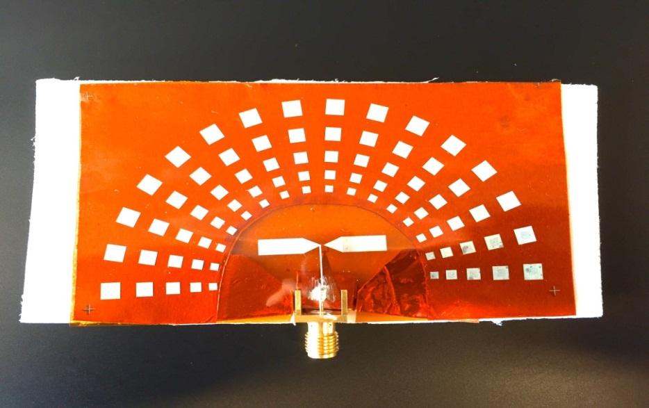
16 Electronic Printing: Capillary-Based System Sonoplot System Capillary dispensing system Ultrasonic pumping to dispense fluid Can pattern materials in fluid form CAD driven 10 micron minimum features Vendor is Sonoplot Inc. Printed 4-element patch antenna array


17 Electronic Printing: Aerosol Jet System 4 Non-contact deposition, 2-7 mm standoff height from nozzle tip to substrate surface Standoff provides flexibility for printing over 3D surfaces many packaging applications Tight Dep. Beam (~10μm to 2.5mm) Optomec system printing antenna array


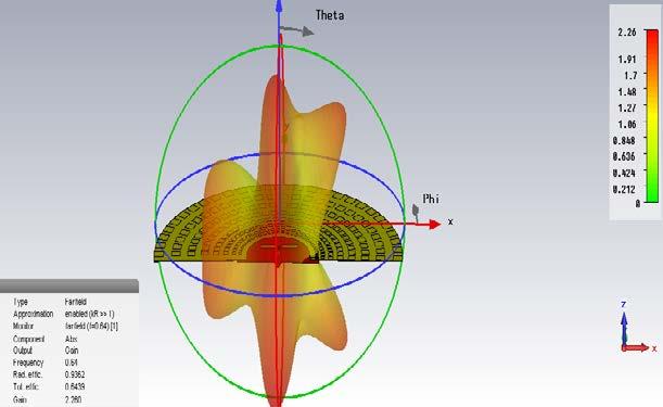
18 Flexible Patch Antenna Array Model developed to predict performance of patch antenna array as a function of bending Joint RTN-UML publication Antennas printed on Kapton Experimental characterization in progress Design and Analysis of 16 GHz Cylindrical Conformal 1x2 Microstrip Patch Antenna Array, Lal Mohan Bhowmik, Craig A. Armiento, William Miniscalco Jagannath Chirravuri, Christopher McCarroll and Alkim Akyurtlu, 2013 Phased Array Radar Conference, Waltham, MA,


19 Printed Metamaterials for Frequency Selective Surfaces (FSS) Goal: Use Metamaterial concepts to tailor the electromagnetic behavior of devices such as a Frequency Selective Surface (FSS) or antenna. Metamaterials are made up of periodic arrays of metallic resonant elements. Both the size of the element and the unit cell are small relative to the wavelength. A FSS designed to reflect, transmit or absorb electromagnetic fields at specific frequencies. Two-sided FSS design with coupling capacitors between unit cells Printed FSS FSS Frequency of operation can be changed by changing capacitance value using different dielectrics. Tunability possible by use of ferroelectrics inks.

20 Greek Theatre Metasurface Antenna Design Simulation Print


21 CNT Transistor: Bottom Gate Design CNT network CNT network Al 2 O 3 Ag Nanoink
 spacing Future Transistors")

22 Improvements for CNT Transistors Current Printed Transistors Random CNT network 200 mm Source-Drain (S-D) spacing Future Transistors Aligned CNT network CNTs span S-D 10 mm S-D spacing Use techniques for CNT Alignment Work with vendors to develop better CNT inks (semiconducting)


23 Hybrid Chip Integration Printed conductive traces may provide an alternative to conventional wire bonding Could be important for microwave applications - controlled impedance up to the chip bonding pad 23

24 Packaging Applications Using Aerosol Jet: Stacked Die Interconnects Printed interconnects between stacked die Courtesy of Optomec Inc. 24
 Resistors Courtesy of Optomec Inc.")
25 Packaging Applications Using Aerosol Jet: Printed Resistors Printed High Tolerance (<5%) Resistors Courtesy of Optomec Inc. 25

 Need better surface finish to integrate electronics Need conductive plastic filament materials for")
26 3D Printing with Hybrid Chip Integration Vivaldi Antenna Array LNA electronics Printed conductive trace on 3D-printed surface Surfaces not flat enough for fine conductive traces Using 3D printer to create physical structure of antenna array Developing selective approaches for patterning metal on array Developing Chip attach and printed interconnect on ABS Funded by Phase 1 of an STTR (with SI2 Technologies & RTN) Need better surface finish to integrate electronics Need conductive plastic filament materials for conductive vias 26
27 Summary: Printed Electronics at UML UML is developing a printed electronics capability with a focus on DoD applications in the RF/microwave domain PE research will be done in partnership with corporate partners such as Raytheon in RURI UML is developing the supply chain for PE in the defense cluster with PERC leveraging a match from the state of Massachusetts. PERC will enable teaming between companies to pursue federal funding opportunities PE Research at UML will exploit unique campus capabilities in nanomanufacturing and control of plastic films for substrates
28 Thank You
Printed Electronics and Additive Microelectronic Packaging For RF/Microwave Applications
 Printed Electronics and Additive Microelectronic Packaging For RF/Microwave Applications Prof. Craig Armiento University of Massachusetts Lowell Raytheon UMass Lowell Research Institute (RURI) Printed
MID Manufacturing Process.
 3D Aerosol Jet Printing An Emerging MID Manufacturing Process. Dr. Martin Hedges Neotech Services MTP, Nuremberg, Germany info@neotechservices.com Aerosol Jet Printing Aerosol Jet Process Overview Current
Flexible Hybrid Electronics Fabricated with High-Performance COTS ICs using RTI CircuitFilm TM Technology
 Flexible Hybrid Electronics Fabricated with High-Performance COTS ICs using RTI CircuitFilm TM Technology Scott Goodwin 1, Erik Vick 2 and Dorota Temple 2 1 Micross Advanced Interconnect Technology Micross
Low Temperature Integration of Thin Films and Devices for Flexible and Stretchable Electronics
 Low Temperature Integration of Thin Films and Devices for Flexible and Stretchable Electronics Pooran Joshi, Stephen Killough, and Teja Kuruganti Oak Ridge National Laboratory FIIW 2015 Displays and PV
University of Texas at Austin, Austin, TX ABSTRACT
 Phase Shifter using Carbon Nanotube Thin-Film Transistor for Flexible Phased-Array Antenna Daniel Pham 1, Harish Subbaraman 2, Maggie Yihong Chen 3, Xiaochuan Xu 1, and Ray T. Chen 1 1 Microelectronics
CHAPTER 6 CARBON NANOTUBE AND ITS RF APPLICATION
 CHAPTER 6 CARBON NANOTUBE AND ITS RF APPLICATION 6.1 Introduction In this chapter we have made a theoretical study about carbon nanotubes electrical properties and their utility in antenna applications.
Accelerating Scale Up of Large Area Electronics
 Accelerating Scale Up of Large Area Electronics Duncan Lindsay Business Development Director, CPI 2015 Centre for Process Innovation Limited. All Rights Reserved. Who are CPI? CPI is a UK technology innovation
Aerosol Jet technology opportunities
 Aerosol Jet technology opportunities Jiří Navrátil 1. Introduction history and formation 2. Aerosol Jet system 2.1 System components 2.2 Inks and substrates 3. Application of Aerosol Jet technology 4.
Passive Direct Print Sensors
 Passive Wireless Sensor Technology Workshop June 6-7, 2012 Hyatt Regency, La Jolla, CA Passive Direct Print Sensors Mike Newton mnewton@nscrypt.com nscrypt Inc. Orlando, Florida University of Texas at
shaping global nanofuture ULTRA-PRECISE PRINTING OF NANOMATERIALS
 shaping global nanofuture ULTRA-PRECISE PRINTING OF NANOMATERIALS WHO ARE WE? XTPL S.A. is a company operating in the nanotechnology segment. The interdisciplinary team of XTPL develops on a global scale
National Centre for Flexible Electronics
 National Centre for Flexible Electronics Tripartite Partnership Government FlexE Centre - A platform for a meaningful interaction between industry and academia. An interdisciplinary team that advances
Printed and Hybrid Integration
 Printed and Hybrid Integration Neil Chilton PhD Technical Director, Printed Electronics Limited, UK Neil.Chilton@PrintedElectronics.com Printed Electronics Limited (PEL) General Overview PEL was founded
Printed Electronics Product Types & Markets. Vince Cahill, VCE Solutions
 Printed Electronics Product Types & Markets Vince Cahill, VCE Solutions Printed Electronic Product Types Printed circuits boards Printed logic / memory Printed batteries Membrane switches Photovoltaics
MEMS in ECE at CMU. Gary K. Fedder
 MEMS in ECE at CMU Gary K. Fedder Department of Electrical and Computer Engineering and The Robotics Institute Carnegie Mellon University Pittsburgh, PA 15213-3890 fedder@ece.cmu.edu http://www.ece.cmu.edu/~mems
C Sensor Systems. THz System Technology and. Prof. Dr.-Ing. Helmut F. Schlaak
 THz System Technology and C Sensor Systems Prof. Dr.-Ing. Helmut F. Schlaak Fachgebiet Mikrotechnik und Elektromechanische Systeme Fachbereich Elektrotechnik und Informationstechnik Technische Universität
PRINTED ELECTRONICS TECHNOLOGIES
 PRINTED ELECTRONICS TECHNOLOGIES YEARS OF R&D DRIVEN BY CONTINUOUS INNOVATION HAVE POSITIONNED GGI SOLUTIONS AS A LEADER IN PRINTED ELECTRONICS TECHNOLOGIES 2 As a level 1 member of the Printable Electronics
Nanotechnology, the infrastructure, and IBM s research projects
 Nanotechnology, the infrastructure, and IBM s research projects Dr. Paul Seidler Coordinator Nanotechnology Center, IBM Research - Zurich Nanotechnology is the understanding and control of matter at dimensions
Micro-sensors - what happens when you make "classical" devices "small": MEMS devices and integrated bolometric IR detectors
 Micro-sensors - what happens when you make "classical" devices "small": MEMS devices and integrated bolometric IR detectors Dean P. Neikirk 1 MURI bio-ir sensors kick-off 6/16/98 Where are the targets
Energy & Space. International Presentations
 Energy & Space International Presentations 2012-2013 Advanced Electronics 3D Printed Circuit Boards 3D Printed Circuit Boards for Solder-Free Printable Electronics 4x4 Vehicles Arduino WiFi Android Controllers
PILOT LINE FOR LARGE-AREA PRINTING OF ELECTRONIC AND PHOTONIC DEVICES. Simon Perraud, Ph.D. Vice president for European affairs
 PILOT LINE FOR LARGE-AREA PRINTING OF ELECTRONIC AND PHOTONIC DEVICES Simon Perraud, Ph.D. Vice president for European affairs ABOUT LITEN Liten is the research institute of CEA devoted to clean energy
ICT Micro- and nanoelectronics technologies
 EPoSS Proposers' Day, 2 Feb 2017, Brussels ICT 31-2017 Micro- and nanoelectronics technologies Eric Fribourg-Blanc, Henri Rajbenbach, Andreas Lymberis European Commission DG CONNECT (Communications Networks,
Electromagnetic Applications in Nanotechnology
 Electromagnetic Applications in Nanotechnology Carbon nanotubes (CNTs) Hexagonal networks of carbon atoms 1nm diameter 1 to 100 microns of length Layer of graphite rolled up into a cylinder Manufactured:
Smart Devices of 2025
 Smart Devices of 2025 Challenges for Packaging of Future Device Technologies Steve Riches/Kevin Cannon Tribus-D Ltd CW Workshop 27 March 2018 E:mail: info@tribus-d.uk M: 07804 980 954 Assembly Technology
In 1984, a cell phone in the U.S. cost $3,995 and
 In 1984, a cell phone in the U.S. cost $3,995 and weighed 2 pounds. Today s 8GB smartphones cost $199 and weigh as little as 4.6 oz. Technology Commercialization Applied Materials is one of the most important
Recent Developments in Multifunctional Integration. Stephan Guttowski, Head of Technology Park»Heterointegration«, Fraunhofer FMD
 Recent Developments in Multifunctional Integration Stephan Guttowski, Head of Technology Park»Heterointegration«, Fraunhofer FMD Founding Participants 2 One-Stop-Shop for developments from wafer technologies
Printable, Novel CNT Inks with V2V Technology
 Printable, Novel CNT Inks with V2V Technology William J. Hurley, Jr., PhD Chasm Technologies, Inc. Canton, MA June 23, 2010 New England Nanomanufacturing Summit 1 Outline CHASM Overview Alliance with SWeNT
Micro-PackS, Technology Platform. Security Characterization Lab Opening
 September, 30 th 2008 Micro-PackS, Technology Platform Security Characterization Lab Opening Members : Micro-PackS in SCS cluster From Silicium to innovative & commucating device R&D structure, gathering
Gain Slope issues in Microwave modules?
 Gain Slope issues in Microwave modules? Physical constraints for broadband operation If you are a microwave hardware engineer you most likely have had a few sobering experiences when you test your new
NextFlex: Enabling a Domestic Manufacturing Ecosystem for Flexible Hybrid Electronics (Extended Abstract)
") NextFlex: Enabling a Domestic Manufacturing Ecosystem for Flexible Hybrid Electronics (Extended Abstract) Benjamin J. Leever*, Eric W. Forsythe + *Air Force Research Laboratory, 2179 12th St., B652/R122,
NextFlex: Enabling a Domestic Manufacturing Ecosystem for Flexible Hybrid Electronics (Extended Abstract) Benjamin J. Leever*, Eric W. Forsythe + *Air Force Research Laboratory, 2179 12th St., B652/R122,
Investigating the Electronic Behavior of Nano-materials From Charge Transport Properties to System Response
 Investigating the Electronic Behavior of Nano-materials From Charge Transport Properties to System Response Amit Verma Assistant Professor Department of Electrical Engineering & Computer Science Texas
Heterogeneous integration of autonomous smart films based on electrochromic transistors
 of autonomous smart films NEWSLETTER #5 www.smartwww.smart-ec.eu Objectives SMART-EC has finalized last August 2014; it aimed at the development of self-powered electrochromic (EC) display device with
3D and Aerosol Printed Conductor Dielectric Full- 3D RF Metamaterials
 3D and Aerosol Printed Conductor Dielectric Full- 3D RF Metamaterials June 22, 2017 Jimmy Hester, Evan Nguyen, Jesse Tice, and Vesna Radisic Approved for Public Release: NG17-1180, 6/2/17 Outline Introduction
EU Research project proposals (call for Finnish companies)
") EU Research project proposals (call for Finnish companies) 11th EEMELI Workshop 29 th August 2012 Jukka Hast Research Professor VTT Technical Research Centre of Finland 04/10/2012 2 General ICT theme work
EU Research project proposals (call for Finnish companies) 11th EEMELI Workshop 29 th August 2012 Jukka Hast Research Professor VTT Technical Research Centre of Finland 04/10/2012 2 General ICT theme work
A Miniaturized Multi-Channel TR Module Design Based on Silicon Substrate
 Progress In Electromagnetics Research Letters, Vol. 74, 117 123, 2018 A Miniaturized Multi-Channel TR Module Design Based on Silicon Substrate Jun Zhou 1, 2, *, Jiapeng Yang 1, Donglei Zhao 1, and Dongsheng
RF/Microwave Circuits I. Introduction Fall 2003
 Introduction Fall 03 Outline Trends for Microwave Designers The Role of Passive Circuits in RF/Microwave Design Examples of Some Passive Circuits Software Laboratory Assignments Grading Trends for Microwave
11:20-13:00 Lunch 14:20-16:00. WS-01 GaN HEMT Characterization and Modeling for micro- and mm-wave Power Amplifier Applications
 CONFERENCE WORKSHOPS SESSIONS AND SHORT MATRIX COURSES - SUNDAY 09:00-10:40 11:20-13:00 Lunch 14:20-16:00 16:40-18:20 WS-01 GaN HEMT Characterization and Modeling for micro- and mm-wave Power Amplifier
Processes for Flexible Electronic Systems
 Processes for Flexible Electronic Systems Michael Feil Fraunhofer Institut feil@izm-m.fraunhofer.de Outline Introduction Single sheet versus reel-to-reel (R2R) Substrate materials R2R printing processes
Large Area, Flexible Electronics TWG. Chair: Dan Gamota, Jabil
 Large Area, Flexible Electronics TWG Chair: Dan Gamota, Jabil Large Area Flexible Electronics Roadmap History 09/2005 inemi Stakeholders identify Flexible Electronics as Future Growth Market and authorize
Consortium Capabilities
 Consortium Capabilities The driver in advanced materials development is to create products with competitive advantages. Products must continuously become faster, lighter and cheaper and must provide additional
FRAUNHOFER INSTITUTE FOR PHOTONIC MICROSYSTEMS IPMS. Application Area. Quality of Life
 FRAUNHOFER INSTITUTE FOR PHOTONIC MICROSYSTEMS IPMS Application Area Quality of Life Overlay image of visible spectral range (VIS) and thermal infrared range (LWIR). Quality of Life With extensive experience
The Future for Printed Electronics
 The Future for Printed Electronics Jon Helliwell National Centre for Printable Electronics 24 October, 2013 Copyright CPI 2013. All rights reserved What is Printed Electronics? Organic and printed electronics
On-body Antenna Design using Carbon Nanotubes
 On-body Antenna Design using Carbon Nanotubes Presenter: Syed Muzahir Abbas, Ph.D. Student Supervisor: Prof. Karu Esselle Centre for Electromagnetic and Antenna Engineering (CELANE) Department of Engineering
B. Flip-Chip Technology
 B. Flip-Chip Technology B1. Level 1. Introduction to Flip-Chip techniques B1.1 Why flip-chip? In the development of packaging of electronics the aim is to lower cost, increase the packaging density, improve
Здра вствуйте, това рищи!
 Manufacturing of Smart Objects by Printing Technologies Здра вствуйте, това рищи! Moscow / RUS, June 05, 2013 Reinhard R. Baumann Chemnitz University of Technology Chair of Digital Printing Fraunhofer
Herzlich willkommen. Druckbare Sensoren für Food Packaging ICT-Agri-Food Symposium. Sören Fricke Section Head Large Area & Flexible Systems
 Herzlich willkommen Druckbare Sensoren für Food Packaging ICT-Agri-Food Symposium Sören Fricke Section Head Large Area & Flexible Systems Agroscope Tänikon, 05.09.2017 Motivation Printed Sensors can be
MEMS for RF, Micro Optics and Scanning Probe Nanotechnology Applications
 MEMS for RF, Micro Optics and Scanning Probe Nanotechnology Applications Part I: RF Applications Introductions and Motivations What are RF MEMS? Example Devices RFIC RFIC consists of Active components
Using Sonnet EM Analysis with Cadence Virtuoso in RFIC Design. Sonnet Application Note: SAN-201B July 2011
 Using Sonnet EM Analysis with Cadence Virtuoso in RFIC Design Sonnet Application Note: SAN-201B July 2011 Description of Sonnet Suites Professional Sonnet Suites Professional is an industry leading full-wave
Flexible Hybrid Electronics The Tipping Point To Drive Printed Electronics Market Growth
 Flexible Hybrid Electronics The Tipping Point To Drive Printed Electronics Market Growth November 7, 2016 Jason Marsh Director of Technology America s Flexible Hybrid Electronics Manufacturing Institute
UNCLASSIFIED. UNCLASSIFIED Air Force Page 1 of 13 R-1 Line #1
 Exhibit R-2, RDT&E Budget Item Justification: PB 2015 Air Force Date: March 2014 3600: Research, Development, Test & Evaluation, Air Force / BA 1: Basic Research COST ($ in Millions) Prior Years FY 2013
Application Interest Group (AIG) Process Overview. Dr. Robert C. Pfahl Director of Roadmapping
 Process Overview. Dr. Robert C. Pfahl Director of Roadmapping") Application Interest Group (AIG) Process Overview Dr. Robert C. Pfahl Director of Roadmapping Outline Overview of IPSR AIG Process Roadmapping Technical Planning Application Interest Group (AIG) Formation
Application Interest Group (AIG) Process Overview Dr. Robert C. Pfahl Director of Roadmapping Outline Overview of IPSR AIG Process Roadmapping Technical Planning Application Interest Group (AIG) Formation
FLEXIBLE HYBRID ELECTRONICS FOR ADDITIVE MANUFACTURING
 FLEXIBLE HYBRID ELECTRONICS FOR ADDITIVE MANUFACTURING JASON MARSH NEXTFLEX CTO JUNE 13 2017 WHAT IS NEXTFLEX? 6/13/2017 PAGE 1 PART OF A NETWORK OF MANUFACTURING INSTITUTES Across the Manufacturing USA
Advancing Consumer Packaging Through Printable Electronics
 IPST Executive Conference, Atlanta, GA March 9-10, 2011 Advancing Consumer Packaging Through Printable Electronics Bernard Kippelen Professor, School of Electrical and Computer Engineering Director, Center
R&D Requirements from the 2004 inemi Roadmap. April 7, 2005 Dr. Robert C. Pfahl, Jr. VP of Operations, inemi
 R&D Requirements from the 2004 inemi Roadmap April 7, 2005 Dr. Robert C. Pfahl, Jr. VP of Operations, inemi Topics Covered Overview of inemi and the 2004 Roadmap Situation Analysis Highlights from the
RFID. Presented by BESSER ASSOCIATES. Instructor: Al Scott
 RFID Presented by BESSER ASSOCIATES Instructor: Al Scott 1 COURSE OUTLINE Uses of RFID Basic RFID System ISM Frequency Bands Walmart Directive EPC RFID System How RF part of EPC System Works RF antennas
Novel Packaging Approaches for Miniature Antennas
 Novel Packaging Approaches for Miniature Antennas Will McKinzie, Greg Mendolia, and John Dutton Etenna Corporation 6100-C Frost Place, Laurel, MD 20707 wmckinzie@etenna.com, gmendolia@etenna.com, and jdutton@etenna.com
Efficient Metasurface Rectenna for Electromagnetic Wireless Power Transfer and Energy Harvesting
 Progress In Electromagnetics Research, Vol. 161, 35 40, 2018 Efficient Metasurface Rectenna for Electromagnetic Wireless Power Transfer and Energy Harvesting Mohamed El Badawe and Omar M. Ramahi * Abstract
Parameter Frequency Typ (GHz) See page 7 for minimum performance specs of AMM7602UC connectorized modules. Description Green Status
 See page 7 for minimum performance specs of AMM7602UC connectorized modules. Description Green Status") The is a broadband MMIC LO buffer amplifier that efficiently provides high gain and output power over a 20-55 GHz frequency band. It is designed to provide a strong, flat output power response when driven
The is a broadband MMIC LO buffer amplifier that efficiently provides high gain and output power over a 20-55 GHz frequency band. It is designed to provide a strong, flat output power response when driven
David B. Miller Vice President & General Manager September 28, 2005
 Electronic Technologies Business Overview David B. Miller Vice President & General Manager September 28, 2005 Forward Looking Statement During the course of this meeting we may make forward-looking statements.
Brief Introduction of Sigurd IC package Assembly
 Brief Introduction of Sigurd IC package Assembly Content Package Development Trend Product Brief Sawing type QFN Representative MEMS Product LGA Light Sensor Proximity Sensor High Yield Capability Low
Challenges in Imaging, Sensors, and Signal Processing
 Challenges in Imaging, Sensors, and Signal Processing Raymond Balcerak MTO Technology Symposium March 5-7, 2007 1 Report Documentation Page Form Approved OMB No. 0704-0188 Public reporting burden for the
Parameter Frequency Typ Min (GHz)
") The is a broadband MMIC LO buffer amplifier that efficiently provides high gain and output power over a 20-55 GHz frequency band. It is designed to provide a strong, flat output power response when driven
The is a broadband MMIC LO buffer amplifier that efficiently provides high gain and output power over a 20-55 GHz frequency band. It is designed to provide a strong, flat output power response when driven
IBM Research - Zurich Research Laboratory
 October 28, 2010 IBM Research - Zurich Research Laboratory Walter Riess Science & Technology Department IBM Research - Zurich wri@zurich.ibm.com Outline IBM Research IBM Research Zurich Science & Technology
Holst Centre Wireless Autonomous Sensor Technologies & Flexible Electronics
 February 10, 2011 Holst Centre Wireless Autonomous Sensor Technologies & Flexible Electronics Presentation overview -General overview -Research focus < 4 Holst Centre: a solid partner in research Independent,
ULTRA LOW CAPACITANCE SCHOTTKY DIODES FOR MIXER AND MULTIPLIER APPLICATIONS TO 400 GHZ
 ULTRA LOW CAPACITANCE SCHOTTKY DIODES FOR MIXER AND MULTIPLIER APPLICATIONS TO 400 GHZ Byron Alderman, Hosh Sanghera, Leo Bamber, Bertrand Thomas, David Matheson Abstract Space Science and Technology Department,
Printing Beyond Color. Printed Smart Objects on Advanced Paper Substrates. Reinhard R. Baumann
 Printing Beyond Color Printed Smart Objects on Advanced Paper Substrates June 17, 2009 member of Reinhard R. Baumann member of Chemnitz University of Technology Institute for Print and Media Technology
The wireless industry
 From May 2007 High Frequency Electronics Copyright Summit Technical Media, LLC RF SiP Design Verification Flow with Quadruple LO Down Converter SiP By HeeSoo Lee and Dean Nicholson Agilent Technologies
Flexible Hybrid Electronics (FHE) Overview
 Overview") Flexible Hybrid Electronics (FHE) Overview in cooperation with NextFlex Manufacturing Institute Date: 12 March 2018 By: John Kornitsky CMTC-FHE Practice Lead @ NextFlex Mfg USA Institute Imagine... If
Flexible Hybrid Electronics (FHE) Overview in cooperation with NextFlex Manufacturing Institute Date: 12 March 2018 By: John Kornitsky CMTC-FHE Practice Lead @ NextFlex Mfg USA Institute Imagine... If
COURSE 2. Mechanical Engineering at MIT
 COURSE 2 Mechanical Engineering at MIT The Department of Mechanical Engineering MechE embodies the Massachusetts Institute of Technology s motto mens et manus, mind and hand as well as heart by combining
Serving Diversified Markets F1Q10
 Corporate Overview Microsemi Today Global Supplier of Semiconductor & Electronic Systems Founded 1960. 50 years of success Nasdaq - MSCC Specializing in System-engineered analog mixed signal integrated
UNCLASSIFIED R-1 ITEM NOMENCLATURE
 Exhibit R-2, RDT&E Budget Item Justification: PB 2014 Air Force DATE: April 2013 COST ($ in Millions) All Prior FY 2014 Years FY 2012 FY 2013 # Base FY 2014 FY 2014 OCO ## Total FY 2015 FY 2016 FY 2017
Compound Semiconductor Applica2ons Catapult Technology Scotland, 4 th May 2016
 Compound Semiconductor Applica2ons Catapult Technology Scotland, 4 th May 2016 Andy Sellars, MBA, PhD, MSc Lead Technologist, Manufacturing & Materials andy.sellars@innovateuk.gov.uk @andy_g_sellars Delivery
Loop Antenna and Rectifier Design for RF Energy Harvesting at 900MHz
 Loop Antenna and Rectifier Design for RF Energy Harvesting at 900MHz Rahul Sharma 1, P.K. Singhal 2 1PG Student, Department of electronis, Madhav Institute of Technology and Sciency, Gwalior-474005, India
Emerging Print Technologies & Applications
 Emerging Print Technologies & Applications By: Pivotal Resources USA, Inc. 2901 Richmond Road #353 Lexington, KY 40509 (859) 230-0093 2013 PRIMIR/NPES EMERGING PRINT TECHNOLOGIES & APPLICATIONS TABLE OF
Ubiquitous Displays and Sensors Activating Surfaces with Flexible Electronics. Dean Baker, Director FlexEnable. APAC Innovation Summit 2016, Hong Kong
 Ubiquitous Displays and Sensors Activating Surfaces with Flexible Electronics Dean Baker, Director FlexEnable, Hong Kong Activating surfaces with flexible displays and sensors Flexible Plastic Displays
GLOBAL MARKETS, TECHNOLOGIES AND MATERIALS FOR THIN AND ULTRATHIN FILMS
 GLOBAL MARKETS, TECHNOLOGIES AND MATERIALS FOR THIN AND ULTRATHIN FILMS SMC057C August Margareth Gagliardi Project Analyst ISBN: 1-62296-338-5 BCC Research 49 Walnut Park, Building 2 Wellesley, MA 02481
Open Innovation to Manage Risks in Technology The Business of Breakthroughs
 Open Innovation to Manage Risks in Technology The Business of Breakthroughs Janos Veres, Program Manager 2016 PARC, All rights reserved. PARC Legacy: A Storied History of Inventing the Future 1970 1973
Progress Towards Computer-Aided Design For Complex Photonic Integrated Circuits
 Department of Electrical and Computer Engineering Progress Towards Computer-Aided Design For Complex Photonic Integrated Circuits Wei-Ping Huang Department of Electrical and Computer Engineering McMaster
Horizon 2020 and Photonics
 Brussels, 13 December 2013 Horizon 2020 and Photonics Thomas Skordas Head of the Photonics Unit, DG CONNECT European Commission Thomas.Skordas@ec.europa.eu Horizon 2020 Horizon 2020 Budget: 78.6 B (in
Nanotechnology and its effect on Electronics Manufacturing
 Nanotechnology and its effect on Electronics Manufacturing Dr. Alan Rae Vice President, Market & Business Development, NanoDynamics, Inc. Dr. Robert C. Pfahl, Jr. VP of Operations, inemi Topics Covered
IMPACT OF 450MM ON CMP
 IMPACT OF 450MM ON CMP MICHAEL CORBETT MANAGING PARTNER LINX CONSULTING, LLC MCORBETT@LINX-CONSULTING.COM PREPARED FOR CMPUG JULY 2011 LINX CONSULTING Outline 1. Overview of Linx Consulting 2. CMP Outlook/Drivers
Applied Electromagnetics Laboratory
 Department of ECE Overview of Present and Recent Research Projects http://www.egr.uh.edu/ael/ EM Faculty Ji Chen Ph.D. 1998 U. Illinois David Jackson Ph.D. 1985 UCLA Stuart Long Ph.D. 1974 Harvard Don
MAGNETO-DIELECTRIC COMPOSITES WITH FREQUENCY SELECTIVE SURFACE LAYERS
 MAGNETO-DIELECTRIC COMPOSITES WITH FREQUENCY SELECTIVE SURFACE LAYERS M. Hawley 1, S. Farhat 1, B. Shanker 2, L. Kempel 2 1 Dept. of Chemical Engineering and Materials Science, Michigan State University;
Analysis of Wet Coating Thickness Effect on Transparent Conductive Electrode Performance using Silver Nanowire
 Analysis of Wet Coating Thickness Effect on Transparent Conductive Electrode Performance using Silver Nanowire 2017. 04. 25 Seung-Hyun Lee, PhD Senior Researcher Dept. Printed Electronics Korea Institute
Direct deposition of surface acoustic wave sensors by aerosol jet printing technique
 OPTOMEC EU UGM Direct deposition of surface acoustic wave sensors by aerosol jet printing technique Denis VANDORMAEL, SIRRIS (Belgium) - le centre collectif de l industrie technologique belge Content Introduction
6.776 High Speed Communication Circuits Lecture 6 MOS Transistors, Passive Components, Gain- Bandwidth Issue for Broadband Amplifiers
 6.776 High Speed Communication Circuits Lecture 6 MOS Transistors, Passive Components, Gain- Bandwidth Issue for Broadband Amplifiers Massachusetts Institute of Technology February 17, 2005 Copyright 2005
Silicon Photonics Technology Platform To Advance The Development Of Optical Interconnects
 Silicon Photonics Technology Platform To Advance The Development Of Optical Interconnects By Mieke Van Bavel, science editor, imec, Belgium; Joris Van Campenhout, imec, Belgium; Wim Bogaerts, imec s associated
End-of-line Standard Substrates For the Characterization of organic
 FRAUNHOFER INSTITUTe FoR Photonic Microsystems IPMS End-of-line Standard Substrates For the Characterization of organic semiconductor Materials Over the last few years, organic electronics have become
SEMINAR ON PERSPECTIVES OF NANOTECHNOLOGY FOR RF AND TERAHERTZ ELECTRONICS. February 1, 2013
 SEMINAR ON PERSPECTIVES OF NANOTECHNOLOGY FOR RF AND TERAHERTZ ELECTRONICS February 1, 2013 GuideMr.Harikrishnan A.IAsst ProfessorANJUSEMINAR MICHAEL ONPERSPECTIVES (NSAJEEC013) OF NANOTECHNOLOGY FOR February
EU's contribution to research and innovation in Electronics
 EU's contribution to research and innovation in Electronics Henri.RAJBENBACH@ec.europa.eu Nikolaos.KYRLOGLOU@ec.europa.eu European Commission DG CONNECT (not legally binding presentation) SEMICON Europa-Flex
MEDIA RELEASE FOR IMMEDIATE RELEASE 26 JULY 2016
 MEDIA RELEASE FOR IMMEDIATE RELEASE 26 JULY 2016 A*STAR S IME KICKS OFF CONSORTIA TO DEVELOP ADVANCED PACKAGING SOLUTIONS FOR NEXT-GENERATION INTERNET OF THINGS APPLICATIONS AND HIGH-PERFORMANCE WIRELESS
IC1301 -WiPE. Wireless Power Transmission for Sustainable Electronics. SWG4.1: Space Applications. 25 March 2014
 IC1301 -WiPE Wireless Power Transmission for Sustainable Electronics SWG4.1: Space Applications 25 March 2014 Alexandru Takacs CNRS LAAS, Toulouse, France University of Toulouse III Paul Sabatier, France
Objectives of transmission lines
 Introduction to Transmission Lines Applications Telephone Cable TV (CATV, or Community Antenna Television) Broadband network High frequency (RF) circuits, e.g., circuit board, RF circuits, etc. Microwave
RF simulations with COMSOL
 RF simulations with COMSOL ICPS 217 Politecnico di Torino Aug. 1 th, 217 Gabriele Rosati gabriele.rosati@comsol.com 3 37.93.8 Copyright 217 COMSOL. Any of the images, text, and equations here may be copied
DEVELOPMENT AND PRODUCTION OF HYBRID CIRCUITS FOR MICROWAVE RADIO LINKS
 Electrocomponent Science and Technology 1977, Vol. 4, pp. 79-83 (C)Gordon and Breach Science Publishers Ltd., 1977 Printed in Great Britain DEVELOPMENT AND PRODUCTION OF HYBRID CIRCUITS FOR MICROWAVE RADIO
MEMS and Nanotechnology-Based Sensors and Devices for Communications, Medical and Aerospace Applications
 MEMS and Nanotechnology-Based Sensors and Devices for Communications, Medical and Aerospace Applications A.R. Jha, Ph.D. C) CRC Press J Taylor & Francis Group Boca Raton London New York CRC Press is an
Larry E. Corey Program Manager
 Larry E. Corey Program Manager Advanced RF Sensors Cold War Today High-tech Countable Low-tech Innumerable Proliferated Air Threats Problem: multiple inexpensive air threat assets overwhelm expensive (Patriot-like)
Analytical Study of Tunable Bilayered-Graphene Dipole Antenna
 1 Analytical Study of Tunable Bilayered-Graphene Dipole Antenna James E. Burke RDAR-MEF-S, bldg. 94 1 st floor Sensor & Seekers Branch/MS&G Division/FPAT Directorate U.S. RDECOM-ARDEC, Picatinny Arsenal,
Department of Electrical Engineering University of North Texas
 Name: Shabuktagin Photon Khan UNT ID: 10900555 Instructor s Name: Professor Hualiang Zhang Course Name: Antenna Theory and Design Course ID: EENG 5420 Email: khan.photon@gmail.com Department of Electrical
Silicon Photonics Photo-Detector Announcement. Mario Paniccia Intel Fellow Director, Photonics Technology Lab
 Silicon Photonics Photo-Detector Announcement Mario Paniccia Intel Fellow Director, Photonics Technology Lab Agenda Intel s Silicon Photonics Research 40G Modulator Recap 40G Photodetector Announcement
Introduction: Planar Transmission Lines
 Chapter-1 Introduction: Planar Transmission Lines 1.1 Overview Microwave integrated circuit (MIC) techniques represent an extension of integrated circuit technology to microwave frequencies. Since four