Using Sonnet EM Analysis with Cadence Virtuoso in RFIC Design. Sonnet Application Note: SAN-201B July 2011
|
|
|
- Felix Atkinson
- 6 years ago
- Views:
Transcription


1 Using Sonnet EM Analysis with Cadence Virtuoso in RFIC Design Sonnet Application Note: SAN-201B July 2011
2 Description of Sonnet Suites Professional Sonnet Suites Professional is an industry leading full-wave 3D Planar Electromagnetic (EM) field simulation software based on the Method of Moments (MoM) technique which accounts for all coupling parasitic and radiation effects from DC to THz. It takes full advantage of the mathematically robust and reliable FFT formulation which avoids time consuming, error prone numerical integration. Thus, combining both MoM and FFT, Sonnet provides an added assurance that it will give outstanding accuracy every time on problems that have traditionally been difficult to solve. Problems with high dielectric constant, ultra thin dielectric layers and/or small dimensions with respect to the wavelength are all handled especially well with Sonnet. Sonnet continues to be an indispensable tool for designers involved in RF/Microwave circuits such as mm-wave MMICs, distributed filters, transitions, Low Temperature Co-fired Ceramics, multi-layer RF packages, coplanar waveguides, and antennas. Sonnet Professional Key Benefits Accurately model passive components (inductors, capacitors, resistors) to extract models like s-parameters, RLCK and Q-factor Accurately model multi layer IC interconnects and via structures Generate a technology accurate electrical model for arbitrary layout shapes Quantify parasitic coupling between components, interconnects and vias Include substrate-induced effects like substrate loss and eddy currents Visualize the current flow in components, interconnects and vias Tightly integrate with Cadence Virtuoso, Agilent ADS and Applied Wave Research MWO through embedded APIs Sonnet Professional Key Features FFT based Method of Moments analysis for ultimate reliability and accuracy Easy to learn, easy and efficient to use Only one high precision analysis engine required for full frequency range no need to switch between solvers Patented Conformal Meshing technology for very efficient high accuracy meshing of curved structures Finite thickness modeling for conductors (including advanced N-sheet model) Dielectric bricks for modeling truncated dielectric materials (e.g. MIM capacitor) Adaptive Band Synthesis (ABS) for fast and reliable frequency sweeps with a minimum number of EM samples - more efficient than traditional approaches Easy to use data display for analysis results, including R, L, C, Q evaluation Equation capability for pre-defined or customized calculation on simulated data All configuration and technology setup is menu / dialog based no need to edit configuration text files Remote EM simulation capability Compatible with the LSF cluster and load balancing system for computing clusters Seamless integration with Cadence Virtuoso, Agilent EEsof EDA s ADS, AWR Microwave Office and Analog Office and The Mathworks MATLAB design environments Sonnet Software Inc. is a Cadence Connections partner 2


3 Introduction Sonnet Software s Application Program Interface (API) into the Cadence Virtuoso layout environment allows Cadence users to perform accurate full-wave EM modelling on selected Virtuoso layout, for physical verification of critical components and interconnections. This plug-in solution allows designers to extract a Sonnet EM analysis directly from the layout view. Simulation results are automatically back annotated to the Cadence schematic. High precision electromagnetic (EM) analysis with Sonnet complements the traditional RC extraction tools. With Sonnet, simulation results include all physical effects like high frequency coupling, skin effect, proximity effects, surface waves and radiation. While traditional RC extraction tools like Cadence Assura are optimised to handle full chip extraction, Sonnet analysis is most suitable to rigorously analyze individual components, interconnects and smaller parts of a layout with very high confidence. With Sonnet, you can replace legacy 3D finite element solvers, which are often not integrated into the Cadence design flow and require cumbersome and error prone manual modelling and data transfer. Virtuoso layout Sonnet simulation model SPICE Agilent RFDE Spectre RF Technology (Cadence library) S/Y/Z-parameters Broad band SPICE model w/ symbols Sonnet simulation results 3


4 When to Use Sonnet Professional Analysis The use of electromagnetic analysis with Sonnet Professional is especially valuable in the following design situations: When parasitic coupling is present. Parasitic coupling is not always easy to predict without using electromagnetic analysis. Even elements which are "sufficiently" far apart can suffer from parasitic coupling: inductive or capacitive coupling, resonance effects due to grounding and surface waves that might propagate at the substrate boundary under certain conditions. Sonnet Professional analysis is based on the physical properties of your technology and will account for such physical effects. When accurate circuit models are not available or circuit model parameters are out of range. Model based circuit simulators are based on models for a specific application, with limited parameter range. For example, only selected geometries, substrate types and substrate parameters are available. It is difficult to estimate the error induced by parameter extrapolation, so using models outside their designed parameter range is not suitable for critical applications. Whenever a layout feature cannot be described by a circuit model, due to its geometry or technology, the physics based analysis with Sonnet Professional will provide the answer. An example for this could be a special inductor, capacitor or transformer which is not included in the design kit. Sonnet can be used to analyze those components "on the fly", or generate a full library of component models with trustworthy electrical results. Sonnet Professional Design Process The following steps describe a typical process for creating and simulating a design with Sonnet Professional for Cadence Virtuoso. 1-Define the stack-up and material properties. A simulation model for Sonnet Professional contains a number of layered dielectrics, conductor levels at the interface between dielectric layers and vias to connect different conductor levels. To simulate a layout in Sonnet, these material properties and definitions ("technology") are required. Typically, the EDA support group will define and qualify a technology file for a Cadence library and release that to the RFIC designers. This is an easy and straightforward process once the material properties are known, because that definition is fully driven by menus and dialog boxes. When a designer creates a Sonnet simulation view of a cell, that predefined Sonnet technology file will be automatically loaded from the Cadence library. Substrate Definition 4

, it is necessary to define a finite analysis area (\"box\") and a uniform sampling resolution (\"cell size\").")


5 2-Make Sonnet View. Based on the layout view of a cell, the designer can easily create the Sonnet analysis view for that cell. If the cell layout contains hierarchy, the hierarchy will be resolved to create a flattened Sonnet EM view. The layout view is untouched and unaltered. Make Sonnet View 3-Define the analysis box. With Sonnet's FFT based approach to Method of Moments (MOM), it is necessary to define a finite analysis area ("box") and a uniform sampling resolution ("cell size"). This defines the granularity for the analysis, and usually requires a trade off between analysis time and accuracy. The user defined cell size is very useful to control the meshing density of very complex shapes, to avoid over-meshing the circuit without any need for manual clean-up. 4-Assign port numbers and properties. In Sonnet, circuit ports connect the analysed structure with the outer circuit. Different port types are available for different purposes. Cadence pins can be converted to Sonnet ports fully automatically, based on the defined mapping. Where needed, feed lines will be extended to the boundary of the analysis area automatically, and de-embedded from the analysis results. 5-Define analysis frequencies. Sonnet uses the Method of Moments where the circuit is analyzed at different frequencies of interest. With the unique Adaptive Band Synthesis (ABS) in Sonnet, an accurate wide band response can be obtained from a minimum number of EM simulated data points within a given frequency range. Using ABS, the designer only needs to enter the start and stop frequency. Of course, composite frequency sweeps are also possible, as well as a "DC" point. Define Analysis Frequencies Define Pin to Port Conversion 5

6 6-Define desired output format. The analysis results can be in many different formats such as S/Y/Z parameters, a schematic symbol with ADS or Spectre frequency domain data or a schematic symbol for broad band SPICE extracted data. The designer can define the desired output data before starting the Sonnet EM simulation, or generate the data later as a post processing task after EM analysis has finished. Note: The Broadband Spice Model can only be generated if you have purchased a Broadband Spice Extractor license from Sonnet. Please see your system administrator if you are unsure of the availability of this option. The Broadband Spice feature allows you to create a circuit model which is valid over broad band. The Broadband Spice Extractor generates models that can be used in Spice as a "black box" representing the high frequency behavior of your project. This feature supports PSpice and Cadence Spectre formats. Choosing Output Formats including the Broadband Spice Model The Broadband Spice model is a direct result of a rational polynomial fit to the S- Parameter data. This polynomial is used to generate the equivalent lumped element circuits which may be used as an input to either PSpice or Spectre. Since the S- Parameters are fitted over a wide frequency band, the generated models can be used in circuit simulators for AC sweeps and transient simulations. Sonnet has optimized these models to be causal. The models used are resistors, capacitors, inductors and dependent Voltage and Current sources. 6
.")


 then Creating Broadband Spice Model form will appear upon")
7 7-Save state. Save the current "state" of the analysis settings for later use. This way, all settings can be loaded into a similar project easily. 8-View simulation model in Sonnet (optional). If desired, the designer can take the simulation model as a 2D or 3D view to Sonnet, and review it in the Sonnet model editor. This is especially useful for complex multi layer circuits. The Sonnet interface will keep track of any manual changes, to makes sure that the Virtuoso view and the Sonnet view stay in sync. Save the Analysis Settings 9-Simulate the circuit. The simulation can be started from within Cadence Virtuoso. The Sonnet analysis monitor will show analysis progress and an estimate of the memory requirement and total simulation time. If the Broadband Spice Model was chosen as one of the desired output formats (Step 6) then Creating Broadband Spice Model form will appear upon completion of the EM Analysis. Note: The Broadband Spice Model can only be generated if you have purchased a Broadband Spice Extractor license from Sonnet. Please see your system administrator if you are unsure of the availability of this option. Simulate the Circuit 7


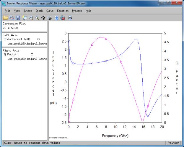
8 10-View simulation results. When the simulation is done, simulation results can be viewed with the Sonnet plotting tool. It is possible to plot any available results while the analysis engine is still computing more frequencies. Parameters like inductor L and Q or capacitor C and Q can be plotted immediately by using pre-defined plot equations. When the current distribution is of interest, the simulation can be configured to store current density data. That data can be visualized in various ways as 2D or 3D graphs. For a better understanding of the circuit, the current density or charge visualization can also be animated over time or frequency. Current density results can be exported to a spread sheet for post processing. In the current density image shown here, note the smooth display of the current distribution, which shows high edge current (required to calculate the conductor losses properly) and current crowding. This is one indication of the high resolution and high precision of the Sonnet analysis result. View Simulation Results 8
 simulation.")

9 11-Back annotate results to the Cadence schematic. When the Sonnet analysis is finished, results are available in different formats. This includes both S/Y/Z-parameters for frequency domain simulation, as well as a broad band SPICE extraction for time domain (SPICE) simulation. Note: The Broadband Spice Model can only be generated if you have purchased a Broadband Spice Extractor license from Sonnet. Please see your system administrator if you are unsure of the availability of this option. Cadence schematic symbols that hold the Sonnet analysis results are created automatically, with all the required mapping files. A sub-circuit schematic for the analyzed cell is also created automatically. Create Cadence models from simulation results Symbol and schematic for the cell 9

10 Example 1 Spiral Inductor on 100 um Silicon (step-graded conductivity in substrate) 5 insulating layers between 1 um and 3 um, thick metal effects modeled. Data and design courtesy of Freescale Semiconductor Measured vs. Calculated red = measured blue = Sonnet result 10

11 Example 2 Spiral Inductor on 100 um Silicon (step-graded conductivity in substrate) 5 insulating layers between 1 um and 3 um, thick metal effects modeled. Data and design courtesy of Freescale Semiconductor Measured vs. Calculated red = measured blue = Sonnet result 11

12 Example turn Circular Spiral Inductor on 100 um Silicon (step-graded conductivity in substrate). 5 insulating layers between 1 um and 3 um, thick metal effects modeled. Data and design courtesy of Freescale Semiconductor Measured vs. Calculated red = measured blue = Sonnet result 12
13 Sonnet Software, Inc. Phone: Toll Free in North America: 877-7SONNET Web: United States Regional Sales: Western US Sales Office: Japan: Sonnet Giken Co., Ltd. Phone: Web: Germany: Muehlhaus Consulting & Software GmbH Phone: +49 (2302) Web: 13
EM Analysis of RFIC Inductors and Transformers. Dr.-Ing. Volker Mühlhaus Dr. Mühlhaus Consulting & Software GmbH, Witten
 EM Analysis of RFIC Inductors and Transformers Dr.-Ing. Volker Mühlhaus, Witten Do you love inductors? Image Kansas State University Inductors from the design kit tend to have the wrong value, optimized
When Should You Apply 3D Planar EM Simulation?
 When Should You Apply 3D Planar EM Simulation? Agilent EEsof EDA IMS 2010 MicroApps Andy Howard Agilent Technologies 1 3D planar EM is now much more of a design tool Solves bigger problems and runs faster
AWR. SIP Flow White Paper UNDERSTANDING AVAILABLE TOOLS FOR RF SYSTEM-IN-PACKAGE AND MULTI-CHIP-MODULE DESIGN AND OPTIMIZATION
 UNDERSTANDING AVAILABLE TOOLS FOR RF SYSTEM-IN-PACKAGE AND MULTI-CHIP-MODULE DESIGN AND OPTIMIZATION RF system-in-package (SiP) and multi-chip-module (MCM) designs present engineers with the challenge
Evaluation of Package Properties for RF BJTs
 Application Note Evaluation of Package Properties for RF BJTs Overview EDA simulation software streamlines the development of digital and analog circuits from definition of concept and estimation of required
--- An integrated 3D EM design flow for EM/Circuit Co-Design
 ADS users group meeting 2009 Rome 13/05, Böblingen 14-15/05, Massy 16/06 --- An integrated 3D EM design flow for EM/Circuit Co-Design Motivations and drivers for co-design Throw-The-Die-Over-The-Wall,
300 frequencies is calculated from electromagnetic analysis at only four frequencies. This entire analysis takes only four minutes.
 Electromagnetic Analysis Speeds RFID Design By Dr. James C. Rautio Sonnet Software, Inc. Liverpool, NY 13088 (315) 453-3096 info@sonnetusa.com http://www.sonnetusa.com Published in Microwaves & RF, February
DATASHEET CADENCE QRC EXTRACTION
 DATASHEET Cadence QRC Etraction, the industry s premier 3D fullchip parasitic etractor that is independent of design style or flow, is a fast and accurate RLCK etraction solution used during design implementation
Design and Matching of a 60-GHz Printed Antenna
 Application Example Design and Matching of a 60-GHz Printed Antenna Using NI AWR Software and AWR Connected for Optenni Figure 1: Patch antenna performance. Impedance matching of high-frequency components
Chapter 2. Inductor Design for RFIC Applications
 Chapter 2 Inductor Design for RFIC Applications 2.1 Introduction A current carrying conductor generates magnetic field and a changing current generates changing magnetic field. According to Faraday s laws
EDA Toolsets for RF Design & Modeling
 Yiannis Moisiadis, Errikos Lourandakis, Sotiris Bantas Helic, Inc. 101 Montgomery str., suite 1950 San Fransisco, CA 94104, USA Email: {moisiad, lourandakis, s.bantas}@helic.com Abstract This paper presents
Examining The Concept Of Ground In Electromagnetic (EM) Simulation
 Simulation") Examining The Concept Of Ground In Electromagnetic (EM) Simulation While circuit simulators require a global ground, EM simulators don t concern themselves with ground at all. As a result, it is the designer
Examining The Concept Of Ground In Electromagnetic (EM) Simulation While circuit simulators require a global ground, EM simulators don t concern themselves with ground at all. As a result, it is the designer
TIME-DOMAIN INTERCONNECT MODELING FOR UWB APPLICATIONS
 TIME-DOMAIN INTERCONNECT MODELING FOR UWB APPLICATIONS Dr. Michael C. Heimlich Director, Consulting Services mike@mwoffice.com Dr. Evgeny Wasserman Development Engineer evgeny@mwoffice.com Ryan Welch Director,
Efficient Electromagnetic Analysis of Spiral Inductor Patterned Ground Shields
 Efficient Electromagnetic Analysis of Spiral Inductor Patterned Ground Shields James C. Rautio, James D. Merrill, and Michael J. Kobasa Sonnet Software, North Syracuse, NY, 13212, USA Abstract Patterned
Synthesis of Optimal On-Chip Baluns
 Synthesis of Optimal On-Chip Baluns Sharad Kapur, David E. Long and Robert C. Frye Integrand Software, Inc. Berkeley Heights, New Jersey Yu-Chia Chen, Ming-Hsiang Cho, Huai-Wen Chang, Jun-Hong Ou and Bigchoug
The wireless industry
 From May 2007 High Frequency Electronics Copyright Summit Technical Media, LLC RF SiP Design Verification Flow with Quadruple LO Down Converter SiP By HeeSoo Lee and Dean Nicholson Agilent Technologies
FDTD SPICE Analysis of High-Speed Cells in Silicon Integrated Circuits
 FDTD Analysis of High-Speed Cells in Silicon Integrated Circuits Neven Orhanovic and Norio Matsui Applied Simulation Technology Gateway Place, Suite 8 San Jose, CA 9 {neven, matsui}@apsimtech.com Abstract
Multilayer VIA simulations using ADS Anurag Bhargava, Application Consultant, Agilent EEsof EDA, Agilent Technologies
 Multilayer VIA simulations using ADS Anurag Bhargava, Application Consultant, Agilent EEsof EDA, Agilent Technologies Many a time designers find themselves in pretty confusing start when it comes to simulating
MMIC/RFIC Packaging Challenges Webcast (July 28, AM PST 12PM EST)
") MMIC/RFIC Packaging Challenges Webcast ( 9AM PST 12PM EST) Board Package Chip HEESOO LEE Agilent EEsof 3DEM Technical Lead 1 Agenda 1. MMIC/RFIC packaging challenges 2. Design techniques and solutions
MMIC/RFIC Packaging Challenges Webcast ( 9AM PST 12PM EST) Board Package Chip HEESOO LEE Agilent EEsof 3DEM Technical Lead 1 Agenda 1. MMIC/RFIC packaging challenges 2. Design techniques and solutions
Using GoldenGate to Verify and Improve Your Designs Using Real Signals
 Using GoldenGate to Verify and Improve Your Designs Using Real Signals Enabling more complete understanding of your designs Agilent EEsof EDA 1 Outline What problems do designers face? Main point of this
Antenna Design: Simulation and Methods
 Antenna Design: Simulation and Methods Radiation Group Signals, Systems and Radiocommunications Department Universidad Politécnica de Madrid Álvaro Noval Sánchez de Toca e-mail: anoval@gr.ssr.upm.es Javier
Free EM Simulator Analyzes Spiral Inductor on Silicon
 Free EM Simulator Analyzes Spiral Inductor on Silicon by James C. Rautio Sonnet Software, Inc. 1020 Seventh North Street, Suite 210 Liverpool, NY 13088 (315)453-3096 info@sonnetusa.com http://www.sonnetusa.com
Efficient Electromagnetic Analysis of Spiral Inductor Patterned Ground Shields. James C. Rautio CEO, Founder Sonnet Software
 Efficient Electromagnetic Analysis of Spiral Inductor Patterned Ground Shields James C. Rautio CEO, Founder Sonnet Software Overview Si RFIC inductors induce current in the Si substrate t by magnetic induction.
Design and Simulation of an ISM Band Antenna on PCB Technology
 Design and Simulation of an ISM Band Antenna on PCB Technology ISM radio bands have traditionally been reserved internationally for the use of radio frequencies (RF) for industrial, scientific, and medical
Accurate Simulation of RF Designs Requires Consistent Modeling Techniques
 From September 2002 High Frequency Electronics Copyright 2002, Summit Technical Media, LLC Accurate Simulation of RF Designs Requires Consistent Modeling Techniques By V. Cojocaru, TDK Electronics Ireland
EMDS for ADS Momentum
 EMDS for ADS Momentum ADS User Group Meeting 2009, Böblingen, Germany Prof. Dr.-Ing. Frank Gustrau Gustrau, Dortmund User Group Meeting 2009-1 Univ. of Applied Sciences and Arts (FH Dortmund) Presentation
Innovations in EDA Webcast Series
 Welcome Innovations in EDA Webcast Series August 2, 2012 Jack Sifri MMIC Design Flow Specialist IC, Laminate, Package Multi-Technology PA Module Design Methodology Realizing the Multi-Technology Vision
Using Analyst TM to Quickly and Accurately Optimize a Chip-Module-Board Transition
 Using Analyst TM to Quickly and Accurately Optimize a Chip-Module-Board Transition 36 High Frequency Electronics By Dr. John Dunn 3D electromagnetic Optimizing the transition (EM) simulators are commonly
Flip-Chip for MM-Wave and Broadband Packaging
 1 Flip-Chip for MM-Wave and Broadband Packaging Wolfgang Heinrich Ferdinand-Braun-Institut für Höchstfrequenztechnik (FBH) Berlin / Germany with contributions by F. J. Schmückle Motivation Growing markets
Cell size and box size in Sonnet RFIC inductor analysis
 Cell size and box size in Sonnet RFIC inductor analysis Purpose of this document: This document describes the effect of some analysis settings in Sonnet: Influence of the cell size Influence of thick metal
Highly Accurate and Robust Automotive Radar System Design. Markus Kopp Lead Application Specialist ANSYS Inc.
 Highly Accurate and Robust Automotive Radar System Design Markus Kopp Lead Application Specialist ANSYS Inc. Introduction This presentation is an overview of a proposed design methodology for automotive
Thank you for downloading one of our ANSYS whitepapers we hope you enjoy it.
 Thank you! Thank you for downloading one of our ANSYS whitepapers we hope you enjoy it. Have questions? Need more information? Please don t hesitate to contact us! We have plenty more where this came from.
A passive circuit based RF optimization methodology for wireless sensor network nodes. Article (peer-reviewed)
") Title Author(s) Editor(s) A passive circuit based RF optimization methodology for wireless sensor network nodes Zheng, Liqiang; Mathewson, Alan; O'Flynn, Brendan; Hayes, Michael; Ó Mathúna, S. Cian Wu,
Title Author(s) Editor(s) A passive circuit based RF optimization methodology for wireless sensor network nodes Zheng, Liqiang; Mathewson, Alan; O'Flynn, Brendan; Hayes, Michael; Ó Mathúna, S. Cian Wu,
Equivalent Circuit Model Overview of Chip Spiral Inductors
 Equivalent Circuit Model Overview of Chip Spiral Inductors The applications of the chip Spiral Inductors have been widely used in telecommunication products as wireless LAN cards, Mobile Phone and so on.
RF Board Design for Next Generation Wireless Systems
 RF Board Design for Next Generation Wireless Systems Page 1 Introduction Purpose: Provide basic background on emerging WiMax standard Introduce a new tool for Genesys that will aide in the design and verification
Figure 1. Inductance
 Tools for On-Chip Interconnect Inductance Extraction Jerry Tallinger OEA International Inc. 155 East Main Ave., Ste. 110 Morgan Hill, CA 95037 jerry@oea.com Haris Basit OEA International Inc. 155 East
RF simulations with COMSOL
 RF simulations with COMSOL ICPS 217 Politecnico di Torino Aug. 1 th, 217 Gabriele Rosati gabriele.rosati@comsol.com 3 37.93.8 Copyright 217 COMSOL. Any of the images, text, and equations here may be copied
MSPP Page 1. MSPP Competencies in SiP Integration for Wireless Applications
 MSPP Page 1 MSPP Competencies in SiP Integration for Wireless Applications MSPP Page 2 Outline Design, simulation and measurements tools MSPP competencies in electrical design and modeling Embedded passive
Lecture 8: Introduction to Hybrid FEM IE
 Lecture 8: Introduction to Hybrid FEM IE 2015.0 Release ANSYS HFSS for Antenna Design 1 2015 ANSYS, Inc. Hybrid FEM-IE Solution Using HFSS and HFSS-IE Advantages of Hybrid Solution Leverage the strength
Modeling Physical PCB Effects 5&
 Abstract Getting logical designs to meet specifications is the first step in creating a manufacturable design. Getting the physical design to work is the next step. The physical effects of PCB materials,
Etched ring absorbing waveguide filter based on a slotted waveguide antenna response
 Etched ring absorbing waveguide filter based on a slotted waveguide antenna response Tinus Stander and Petrie Meyer Department of E&E Engineering University of Stellenbosch Private Bag X1 7602 Matieland
Schematic-Level Transmission Line Models for the Pyramid Probe
 Schematic-Level Transmission Line Models for the Pyramid Probe Abstract Cascade Microtech s Pyramid Probe enables customers to perform production-grade, on-die, full-speed test of RF circuits for Known-Good
Lines and Slotlines. Microstrip. Third Edition. Ramesh Garg. Inder Bahl. Maurizio Bozzi ARTECH HOUSE BOSTON LONDON. artechhouse.
 Microstrip Lines and Slotlines Third Edition Ramesh Garg Inder Bahl Maurizio Bozzi ARTECH HOUSE BOSTON LONDON artechhouse.com Contents Preface xi Microstrip Lines I: Quasi-Static Analyses, Dispersion Models,
Tutorial: Getting Started with RFIC Inductor Toolkit
 Tutorial: Getting Started with RFIC Inductor Toolkit Table of contents: Tutorial: Getting Started with RFIC Inductor Toolkit... 1 Introduction... 2 Installation... 2 Create a new example workspace... 3
Accurate Models for Spiral Resonators
 MITSUBISHI ELECTRIC RESEARCH LABORATORIES http://www.merl.com Accurate Models for Spiral Resonators Ellstein, D.; Wang, B.; Teo, K.H. TR1-89 October 1 Abstract Analytically-based circuit models for two
Signal Integrity Modeling and Simulation for IC/Package Co-Design
 Signal Integrity Modeling and Simulation for IC/Package Co-Design Ching-Chao Huang Optimal Corp. October 24, 2004 Why IC and package co-design? The same IC in different packages may not work Package is
CST s commercial Beam-Physics Codes Ulrich Becker CST (Computer Simulation Technique)
") CST s commercial Beam-Physics Codes Ulrich Becker CST (Computer Simulation Technique) 1 ICAP 2006 Chamonix-Mont Blanc Ulrich Becker www.cst.com Outline Overview CST STUDIO SUITE Accelerator related examples
CST s commercial Beam-Physics Codes Ulrich Becker CST (Computer Simulation Technique) 1 ICAP 2006 Chamonix-Mont Blanc Ulrich Becker www.cst.com Outline Overview CST STUDIO SUITE Accelerator related examples
It s a matter of tradition. RAPID WHOLE - CHIP RF MODELING ñ Inductance-aware RFIC design
 It s a matter of tradition RAPID WHOLE - CHIP RF MODELING ñ Inductance-aware RFIC design Meander border, an ubiquitous ornamental theme in Ancient and Classical Greek pottery painting and architecture.
Index. Cambridge University Press Silicon Photonics Design Lukas Chrostowski and Michael Hochberg. Index.
 absorption, 69 active tuning, 234 alignment, 394 396 apodization, 164 applications, 7 automated optical probe station, 389 397 avalanche detector, 268 back reflection, 164 band structures, 30 bandwidth
Agilent EEsof EDA. Enabling First Pass Success. Chee Keong, Teo Business Development Manager EEsof South Asia. Agilent Restricted
 Agilent EEsof EDA Enabling First Pass Success Chee Keong, Teo Business Development Manager EEsof South Asia EEsof EDA is Strategic to Agilent Technologies As the world s premier measurement company, Agilent
CIRCUITS. Raj Nair Donald Bennett PRENTICE HALL
 POWER INTEGRITY ANALYSIS AND MANAGEMENT I CIRCUITS Raj Nair Donald Bennett PRENTICE HALL Upper Saddle River, NJ Boston Indianapolis San Francisco New York Toronto Montreal London Munich Paris Madrid Capetown
Advanced Meshing Techniques
 Advanced Meshing Techniques Ansoft High Frequency Structure Simulator v10 Training Seminar P-1 Overview Initial Mesh True Surface Approximation Surface Approximation Operations Lambda Refinement Seeding
10 COVER FEATURE CAD/EDA FOCUS
 10 COVER FEATURE CAD/EDA FOCUS Effective full 3D EMI analysis of complex PCBs by utilizing the latest advances in numerical methods combined with novel time-domain measurement technologies. By Chung-Huan
Development of Model Libraries for Embedded Passives Using Network Synthesis
 IEEE TRANSACTIONS ON CIRCUITS AND SYSTEMS II: ANALOG AND DIGITAL SIGNAL PROCESSING, VOL 47, NO 4, APRIL 2000 249 Development of Model Libraries for Embedded Passives Using Network Synthesis Kwang Lim Choi
Modeling Method of circuit exposure to UWB Pulse
 U.S. Army Research, Development and Engineering Command Modeling Method of circuit exposure to UWB Pulse James E. Burke Fuze & Precision, Armaments Technology Directorate, Picatinny Arsenal, NJ 07806-5000
EMC simulation addresses ECU validation issues
 EMC simulation addresses ECU validation issues A more straightforward validation of electromagnetic compatibility can be achieved by combining tools. By Stefan Heimburger, Andreas Barchanski, and Thorsten
Monoconical RF Antenna
 Page 1 of 8 RF and Microwave Models : Monoconical RF Antenna Monoconical RF Antenna Introduction Conical antennas are useful for many applications due to their broadband characteristics and relative simplicity.
ELE3310 Basic Electromagnetics Lab Session 1
 ELE3310 Basic Electromagnetics Lab Session 1 Gao Xin By modifying CST MICROWAVE STUDIO 2006 tutorials Geometric Construction and Solver Settings Introduction and Model Dimensions In this tutorial you will
OPTIMIZED FRACTAL INDUCTOR FOR RF APPLICATIONS
 OPTIMIZED FRACTAL INDUCTOR FOR RF APPLICATIONS B. V. N. S. M. Nagesh Deevi and N. Bheema Rao 1 Department of Electronics and Communication Engineering, NIT-Warangal, India 2 Department of Electronics and
Co-Planar Waveguide (Driven Terminal)
") Co-Planar Waveguide (Driven Terminal) The coplanar waveguide CPW consists of a signal trace sandwiched between two coplanar ground conductors. The width of the signal trace and the gap between the trace
Co-Planar Waveguide (Driven Terminal) The coplanar waveguide CPW consists of a signal trace sandwiched between two coplanar ground conductors. The width of the signal trace and the gap between the trace
ON-CHIP TECHNOLOGY INDEPENDENT 3-D MOD- ELS FOR MILLIMETER-WAVE TRANSMISSION LINES WITH BEND AND GAP DISCONTINUITY
 Progress In Electromagnetics Research B, Vol. 22, 171 185, 2010 ON-CHIP TECHNOLOGY INDEPENDENT 3-D MOD- ELS FOR MILLIMETER-WAVE TRANSMISSION LINES WITH BEND AND GAP DISCONTINUITY G. A. Wang, W. Woods,
Introduction: Planar Transmission Lines
 Chapter-1 Introduction: Planar Transmission Lines 1.1 Overview Microwave integrated circuit (MIC) techniques represent an extension of integrated circuit technology to microwave frequencies. Since four
NI AWR Software AWR. ni.com/awr. ni.com/awr. Product Portfolio
 NI AWR Software Product Portfolio AWR ni.com/awr ni.com/awr NI AWR Software Wireless Design: Trends and Challenges Next-generation wireless devices, communications infrastructure, and aerospace/defense
Microwave and RF Engineering
 Microwave and RF Engineering Volume 1 An Electronic Design Automation Approach Ali A. Behagi and Stephen D. Turner BT Microwave LLC State College, PA 16803 Copyrighted Material Microwave and RF Engineering
COMPACT DESIGN AND SIMULATION OF LOW PASS MICROWAVE FILTER ON MICROSTRIP TRANSMISSION LINE AT 2.4 GHz
 International Journal of Management, IT & Engineering Vol. 7 Issue 7, July 2017, ISSN: 2249-0558 Impact Factor: 7.119 Journal Homepage: Double-Blind Peer Reviewed Refereed Open Access International Journal
ELEC Course Objectives/Proficiencies
 Lecture 1 -- to identify (and list examples of) intentional and unintentional receivers -- to list three (broad) ways of reducing/eliminating interference -- to explain the differences between conducted/radiated
EM Analysis of RFIC Transmission Lines
 EM Analysis of RFIC Transmission Lines Purpose of this document: In this document, we will discuss the analysis of single ended and differential on-chip transmission lines, the interpretation of results
Waveguide Bragg Gratings and Resonators LUMERICAL SOLUTIONS INC
 Waveguide Bragg Gratings and Resonators JUNE 2016 1 Outline Introduction Waveguide Bragg gratings Background Simulation challenges and solutions Photolithography simulation Initial design with FDTD Band
Design and Analysis of Novel Compact Inductor Resonator Filter
 Design and Analysis of Novel Compact Inductor Resonator Filter Gye-An Lee 1, Mohamed Megahed 2, and Franco De Flaviis 1. 1 Department of Electrical and Computer Engineering University of California, Irvine
Methodology for MMIC Layout Design
 17 Methodology for MMIC Layout Design Fatima Salete Correra 1 and Eduardo Amato Tolezani 2, 1 Laboratório de Microeletrônica da USP, Av. Prof. Luciano Gualberto, tr. 3, n.158, CEP 05508-970, São Paulo,
Experimental Analysis of Design Options for Spiral Inductors Integrated on Low Cost MCM-D Substrates
 Experimental Analysis of Design Options for Spiral Inductors Integrated on Low Cost MCM-D Substrates Didier Cottet, Janusz Grzyb, Michael Scheffler, Gerhard Tröster Electronics Laboratory, ETH Zürich Gloriastrasse
Streamlined Design of SiGe Based Power Amplifiers
 ROMANIAN JOURNAL OF INFORMATION SCIENCE AND TECHNOLOGY Volume 13, Number 1, 2010, 22 32 Streamlined Design of SiGe Based Power Amplifiers Mladen BOŽANIĆ1, Saurabh SINHA 1, Alexandru MÜLLER2 1 Department
An EM-aware methodology for a high-speed multi-protocol 28Gbps SerDes design with TSMC 16FFC
 An EM-aware methodology for a high-speed multi-protocol 28Gbps SerDes design with TSMC 16FFC Bud Hunter, SerDes Analog IC Design Manager, Wipro Kelly Damalou, Sr. Technical Account Manager, Helic TSMC
A WIDEBAND RECTANGULAR MICROSTRIP ANTENNA WITH CAPACITIVE FEEDING
 A WIDEBAND RECTANGULAR MICROSTRIP ANTENNA WITH CAPACITIVE FEEDING Hind S. Hussain Department of Physics, College of Science, Al-Nahrain University, Baghdad, Iraq E-Mail: hindalrawi@yahoo.com ABSTRACT A
Low Noise Amplifier Design Methodology Summary By Ambarish Roy, Skyworks Solutions, Inc.
 February 2014 Low Noise Amplifier Design Methodology Summary By Ambarish Roy, Skyworks Solutions, Inc. Low Noise Amplifiers (LNAs) amplify weak signals received by the antenna in communication systems.
Electrical and Thermal Analysis of an OLED Module
 Electrical and Thermal Analysis of an OLED Module Jurica Kundrata and Adrijan Barić University of Zagreb Faculty of Electrical Engineering and Computing COMSOL CONFERENCE 2012. 10.-12. October 2012. Excerpt
Single-turn and multi-turn coil domains in 3D COMSOL. All rights reserved.
 Single-turn and multi-turn coil domains in 3D 2012 COMSOL. All rights reserved. Introduction This tutorial shows how to use the Single-Turn Coil Domain and Multi-Turn Coil Domain features in COMSOL s Magnetic
Methods and Approaches for RF Circuit Simulation And Electromagnetic Modelling
 Methods and Approaches for RF Circuit Simulation And Electromagnetic Modelling T.A.M. Kevenaar 1, E.J.W. ter Maten 1, H.H.J. Janssen 1, S. Onneweer 2 1 Philips Research, Eindhoven, The Netherlands 2 Philips
Agilent EEsof EDA.
 Agilent EEsof EDA This document is owned by Agilent Technologies, but is no longer kept current and may contain obsolete or inaccurate references. We regret any inconvenience this may cause. For the latest
100 Genesys Design Examples
 [Type here] [Type here] [Type here] 100 Genesys Design Examples A Design Approach using (Genesys): Chapter 2: Transmission Line Components Ali Behagi 100 Genesys Design Examples A Design Approach using
Front-To-Back MMIC Design Flow with ADS. Speed MMICs to market Save money and achieve high yield
 Front-To-Back MMIC Design Flow with ADS Speed MMICs to market Save money and achieve high yield 1 Unique Tools for Robust Designs, First Pass, and High Yield Yield Sensitivity Histogram (YSH) to components
Appendix. RF Transient Simulator. Page 1
 Appendix RF Transient Simulator Page 1 RF Transient/Convolution Simulation This simulator can be used to solve problems associated with circuit simulation, when the signal and waveforms involved are modulated
Inductor Modeling of Integrated Passive Device for RF Applications
 Inductor Modeling of Integrated Passive Device for RF Applications Yuan-Chia Hsu Meng-Lieh Sheu Chip Implementation Center Department of Electrical Engineering 1F, No.1, Prosperity Road I, National Chi
Performance Enhancement For Spiral Indcutors, Design And Modeling
 Performance Enhancement For Spiral Indcutors, Design And Modeling Mohammad Hossein Nemati 16311 Sabanci University Final Report for Semiconductor Process course Introduction: How to practically improve
Gain Slope issues in Microwave modules?
 Gain Slope issues in Microwave modules? Physical constraints for broadband operation If you are a microwave hardware engineer you most likely have had a few sobering experiences when you test your new
Reliable World Class Insights Your Silicon Valley Partner in Simulation ANSYS Sales, Consulting, Training & Support
 www.ozeninc.com info@ozeninc.com (408) 732 4665 1210 E Arques Ave St 207 Sunnyvale, CA 94085 Reliable World Class Insights Your Silicon Valley Partner in Simulation ANSYS Sales, Consulting, Training &
Virtual EM Prototyping: From Microwaves to Optics
 Virtual EM Prototyping: From Microwaves to Optics Dr. Frank Demming, CST AG Dr. Avri Frenkel, Anafa Electromagnetic Solutions Virtual EM Prototyping Efficient Maxwell Equations solvers has been developed,
2.5D & 3D Package Signal Integrity A Paradigm Shift
 2.5D & 3D Package Signal Integrity A Paradigm Shift Nozad Karim Technology & Platform Development November, 2011 Enabling a Microelectronic World Content Traditional package signal integrity vs. 2.5D/3D
Research Article Wideband Microstrip 90 Hybrid Coupler Using High Pass Network
 Microwave Science and Technology, Article ID 854346, 6 pages http://dx.doi.org/1.1155/214/854346 Research Article Wideband Microstrip 9 Hybrid Coupler Using High Pass Network Leung Chiu Department of Electronic
Comparison of IC Conducted Emission Measurement Methods
 IEEE TRANSACTIONS ON INSTRUMENTATION AND MEASUREMENT, VOL. 52, NO. 3, JUNE 2003 839 Comparison of IC Conducted Emission Measurement Methods Franco Fiori, Member, IEEE, and Francesco Musolino, Member, IEEE
Research Article Compact and Wideband Parallel-Strip 180 Hybrid Coupler with Arbitrary Power Division Ratios
 Microwave Science and Technology Volume 13, Article ID 56734, 1 pages http://dx.doi.org/1.1155/13/56734 Research Article Compact and Wideband Parallel-Strip 18 Hybrid Coupler with Arbitrary Power Division
Correlation Between Measured and Simulated Parameters of a Proposed Transfer Standard
 Correlation Between Measured and Simulated Parameters of a Proposed Transfer Standard Jim Nadolny AMP Incorporated ABSTRACT Total radiated power of a device can be measured using a mode stirred chamber
S-Parameters Simulation
 S-Parameters Simulation of an RLC filter Description An RLC circuit is an electrical circuit formed of a number of resistors, inductors and capacitors. There are multiple applications for this type of
Conducted EMI Simulation of Switched Mode Power Supply
 Conducted EMI Simulation of Switched Mode Power Supply Hongyu Li #1, David Pommerenke #2, Weifeng Pan #3, Shuai Xu *4, Huasheng Ren *5, Fantao Meng *6, Xinghai Zhang *7 # EMC Laboratory, Missouri University
A Simulation Methodology for Wirebonds Interconnects of Radiofrequency Integrated Circuits
 A Simulation Methodology for Wirebonds Interconnects of Radiofrequency Integrated Circuits Hercílio M. Cavalcanti 1 and Leandro T. Manera 2 1 Hercílio M. Cavalcanti, CTI Renato Archer, Campinas, São Paulo,
EXPERIMENT NUMBER 10 TRANSIENT ANALYSIS USING PSPICE
 EXPERIMENT NUMBER 10 TRANSIENT ANALYSIS USING PSPICE Objective: To learn to use a circuit simulator package for plotting the response of a circuit in the time domain. Preliminary: Revise laboratory 8 to
Projects in microwave theory 2009
 Electrical and information technology Projects in microwave theory 2009 Write a short report on the project that includes a short abstract, an introduction, a theory section, a section on the results and
High-frequency transmission line transitions
 High-frequency transmission line transitions Leonard T. Hall a,b,hedleyj.hansen a,b,c, and Derek Abbott a,b a Centre for Biomedical Engineering, The University of Adelaide, SA 55 Australia b Department
Antennas and Propagation. Chapter 4: Antenna Types
 Antennas and Propagation : Antenna Types 4.4 Aperture Antennas High microwave frequencies Thin wires and dielectrics cause loss Coaxial lines: may have 10dB per meter Waveguides often used instead Aperture
The Design & Test of Broadband Launches up to 50 GHz on Thin & Thick Substrates
 The Performance Leader in Microwave Connectors The Design & Test of Broadband Launches up to 50 GHz on Thin & Thick Substrates Thin Substrate: 8 mil Rogers R04003 Substrate Thick Substrate: 30 mil Rogers
Packaged mm-wave GaN, GaAs and Si ICs for 5G and automotive radar
 Packaged mm-wave GaN, GaAs and Si ICs for 5G and automotive radar Eric Leclerc UMS 1 st Nov 2018 Outline Why heterogenous integration? About UMS Technology portfolio Design tooling: Cadence / GoldenGate