Здра вствуйте, това рищи!
|
|
|
- Gerard Lamb
- 6 years ago
- Views:
Transcription
1 Manufacturing of Smart Objects by Printing Technologies Здра вствуйте, това рищи! Moscow / RUS, June 05, 2013 Reinhard R. Baumann Chemnitz University of Technology Chair of Digital Printing Fraunhofer Institute for Electronic Nano Systems, Chemnitz Business Unit Green and Wireless Dpt. Printed Functionalities 1 Digital Fabrication 2013 Chemnitz University of Technology Prof. Dr. Reinhard R. Baumann
2 Manufacturing of Smart Objects by Printing Technologies Energy Supply for MEMS with Printed Batteries Moscow / RUS, June 05, 2013 Reinhard R. Baumann Chemnitz University of Technology Chair of Digital Printing Fraunhofer Institute for Electronic Nano Systems, Chemnitz Business Unit Green and Wireless Dpt. Printed Functionalities 2 Digital Fabrication 2013 Chemnitz University of Technology Prof. Dr. Reinhard R. Baumann


")


3 Products, Technologies and Services Multi Device Integration Reliability and Security Printed Functionalities Back-End of Line System Packaging Advanced System Engineering NIR / MIR micro spectrometer Nano tomography Printed Power Air gaps Ultrasonic transducer Surface current Microfluidic cartridge Analysis of nanodeformations Printed RFID antennas Through silicon vias (TSV) Nano needles Near field scanner Nanocomposite moisture sensor Stress concentration at a via (FEA) Printed nano sieves Aligned single wall CNTs Interposer Thin Film Packaging Electro magnetic field 3 Digital Fabrication 2013 Chemnitz University of Technology Prof. Dr. Reinhard R. Baumann


 EL OLED Power sources")

4 The Vision : printed smart objects for the internet of things printed sensor 2009 UCSD printed keyboard printed signage elements 2010 Thin Film Electronics AB communication with a computer system RFID technology near field technology Printed power source Memory Thin film memories Printed memories Silicon electronics Communication protocol Measurement functionality Digital logic Organic FETs Electrolytic transistors High frequency rectifiers Power amplifiers Sensors Pressure sensors Keyboards Display Electrochromic Electrophoretic (e-ink) EL OLED Power sources Batteries Solar cells Fuel cells Passive components Antennae UHF & microwave dipoles 4 Digital Fabrication 2013 Chemnitz University of Technology Prof. Dr. Reinhard R. Baumann


5 Print Competences in Chemnitz Energy Systems Supra Balls Inkjet Technicum RFID µ Fluidics Functionality Formation Machinery Devices 5 Digital Fabrication 2013 Chemnitz University of Technology Prof. Dr. Reinhard R. Baumann
6 The Manufacturing Technology Printing Functional Printing Machinery Applications: Printed Smart Objects 6 Digital Fabrication 2013 Chemnitz University of Technology Prof. Dr. Reinhard R. Baumann
7 The Manufacturing Technology Printing Functional Printing Machinery Applications: Printed Smart Objects 7 Digital Fabrication 2013 Chemnitz University of Technology Prof. Dr. Reinhard R. Baumann
8 physical virtual physical Printing Process Chain Creative Process Technical Prepress Data Printing Plate Conventional Printing Digital Printing CMYK Pattern Substrate Postpress / Finishing Printed Product 8 Digital Fabrication 2013 Chemnitz University of Technology Prof. Dr. Reinhard R. Baumann
9 Printing is a general manufacturing technology Printing is an additive technology ink is deposited on the substrate only at positions where its functionality is essential no material removal, no lithography is needed valid for digital printing, batch size 1, setup time 0 Printing is a continuous manufacturing technology in case of web fed, no batch handling easy flexible substrate handling, fiber or plastic based Printing is regularly carried out under ambient conditions no vacuum needed for material deposition clean and/or inert conditions are OK Printing is a highly productive manufacturing technology 9 Digital Fabrication 2013 Chemnitz University of Technology Prof. Dr. Reinhard R. Baumann
10 physical virtual physical Digital Fabrication Process Chain C A D Data Digital Printing Laser Techniques Material Pattern Substrate Postpress / Finishing Printed Product 10 Digital Fabrication 2013 Chemnitz University of Technology Prof. Dr. Reinhard R. Baumann
11 Digital Fabrication - basic topics Opportunities Digital Fabrication product run length 1 change over time 0 Typical DF Technologies Digital Printing Laser Processing their chaining chaining with analogue technologies 11 Digital Fabrication 2013 Chemnitz University of Technology Prof. Dr. Reinhard R. Baumann
12 The Manufacturing Technology Printing Functional Printing Machinery Applications: Printed Smart Objects 12 Digital Fabrication 2013 Chemnitz University of Technology Prof. Dr. Reinhard R. Baumann


13 micro FLEX printing competence in Chemnitz Micromachining for Industrial Applications and R&D 3D-Micromac AG Digital Fabrication 2013 Chemnitz University of Technology Prof. Dr. Reinhard R. Baumann

14 The Manufacturing Technology Printing Functional Printing Machinery Printed Smart Objects Applications: Energy Systems for Pervasive Electronics 14 Digital Fabrication 2013 Chemnitz University of Technology Prof. Dr. Reinhard R. Baumann
15 mobile electronics mobile energy electronics everywhere electronics everywhere POWER everywhere electronics everywhere electronics everywhere 15 Digital Fabrication 2013 Chemnitz University of Technology Prof. Dr. Reinhard R. Baumann
16 BATTERY POWER everywhere 16 Digital Fabrication 2013 Chemnitz University of Technology Prof. Dr. Reinhard R. Baumann

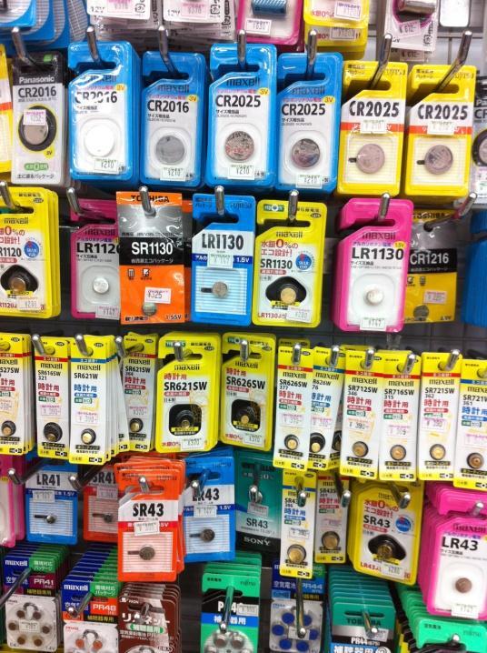
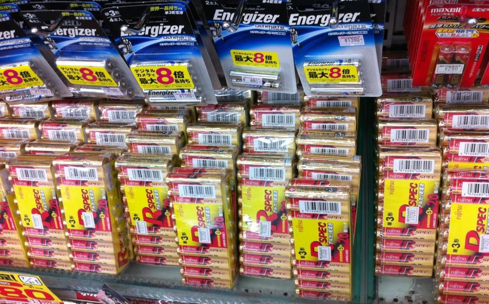
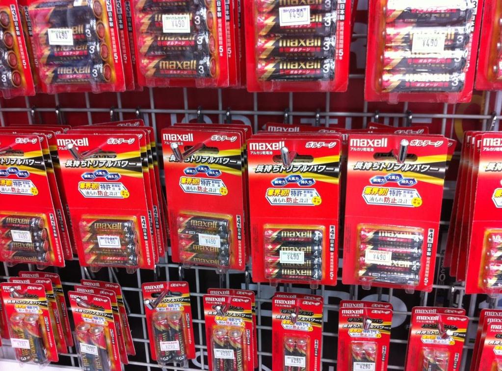
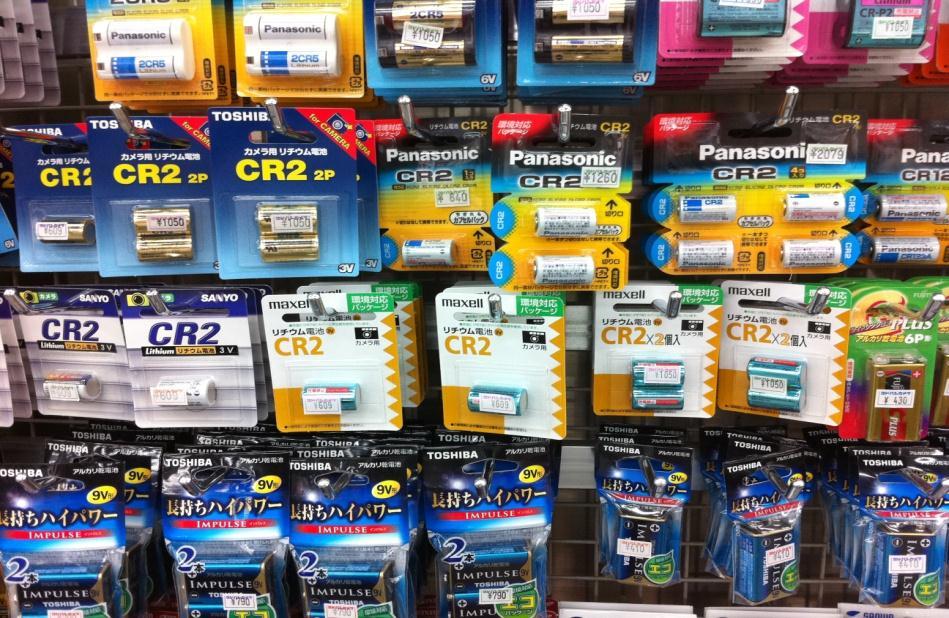

17 BATTERY POWER everywhere 17 Digital Fabrication 2013 Chemnitz University of Technology Prof. Dr. Reinhard R. Baumann


 high layout variability")


18 electronics everywhere Power everywhere Further development of battery technology low price low thickness high flexibility R2R-processable direct product integration possible environmentally friendly ( mercury free) high layout variability flexible displays semi-active RFID-Label data logger health care smart patches smart cards 18 Digital Fabrication 2013 Chemnitz University of Technology Prof. Dr. Reinhard R. Baumann


19 Zinc - Manganese Dioxide Electrochemical Energy Systems D. Linden: Energy storage capabilities of rechargeable battery systems 19 Digital Fabrication 2013 Chemnitz University of Technology Prof. Dr. Reinhard R. Baumann
20 Printing flexible batteries Design Cathode (+) manganese dioxide + solvent + conductive additive Substrate plastic foil ( PET 75 µm) Anode (-) zinc + solvent + conductive additive Separator Current collector graphite + carbon based ink Fig: cross section Electrolyte zinc chloride + gelling agent + additives 20 Digital Fabrication 2013 Chemnitz University of Technology Prof. Dr. Reinhard R. Baumann


21 Printing Flexible Batteries (Zn/MnO 2 ) single cell of 1.5 V nominal voltage discharge current: 200 µa (constant) cut-off voltage: 0.9 V capacity: > 5 mah/cm² (adoptable) thickness: < 1 mm weight: approx. 0.8 g 1,5 V 6 V capacity > 5 mah/cm 2 21 Digital Fabrication 2013 Chemnitz University of Technology Prof. Dr. Reinhard R. Baumann


22 + battery 2 battery 1 Working Assembled Device battery 2 + battery 1 2 primary batteries: 3.0 V nominal voltage 1 printed push button 2 red SMD-LEDs > 1000 cycles (2 s ON, 5 s OFF) 22 Digital Fabrication 2013 Chemnitz University of Technology Prof. Dr. Reinhard R. Baumann


23 Demonstrator 1500 integrated batteries shipped integration in printed products Chemical system: Zn-MnO 2 -ZnCl V cells 23 Digital Fabrication 2013 Chemnitz University of Technology Prof. Dr. Reinhard R. Baumann


24 Series connection of batteries 11 µa 86 µa 266 µa 24 Digital Fabrication 2013 Chemnitz University of Technology Prof. Dr. Reinhard R. Baumann
 upper part lower")

25 Series connection of batteries Setup of 10 stacked battery (15 V nom ) upper part lower part 25 Digital Fabrication 2013 Chemnitz University of Technology Prof. Dr. Reinhard R. Baumann
26 Printed Functionalities Further Related Printing Applications Printed Micro-Fluidic Components 26 Digital Fabrication 2013 Chemnitz University of Technology Prof. Dr. Reinhard R. Baumann


27 Lab-on-Chip analysis of body fluids source of figures: µ and nano filters 4 µ fluidics 27 Digital Fabrication 2013 Chemnitz University of Technology Prof. Dr. Reinhard R. Baumann


, 606 610.")
28 Inkjet manufacturing technology UV curable ink UV light J. Hammerschmidt, E. M. Eck, E. Sowade, S. J. Jahn, S. Ebert, A. Morschhauser, W. A. Goedel: Complete Digital Fabrication of Polymeric Microsieves. NIP26/DF Proceedings, 2010, S. F. Jahn, L. Engisch, R. R. Baumann, S. Ebert, W. A. Goedel: Inkjet fabrication method for polymer microsieves. Langmuir, 2009, 25 (1), Digital Fabrication 2013 Chemnitz University of Technology Prof. Dr. Reinhard R. Baumann


29 Printing of Reinforcing Patterns for Nanosieves J. Hammerschmidt et al.: Complete Digital Fabrication of Polymeric Microsieves Langmuir, Digital Fabrication 2013 Chemnitz University of Technology Prof. Dr. Reinhard R. Baumann
30 Printed Functionalities Where to meet the Functional Printers? 30 Digital Fabrication 2013 Chemnitz University of Technology Prof. Dr. Reinhard R. Baumann


31 Where to meet the Functional Printers? 31 Digital Fabrication 2013 Chemnitz University of Technology Prof. Dr. Reinhard R. Baumann


32 always welcome in Chemnitz, Saxony! Institute for Print and Media Technology thank you for your attention Dpt. Printed Functionalities Prof. Dr. Reinhard R. Baumann 32 Digital Fabrication 2013 Chemnitz University of Technology Prof. Dr. Reinhard R. Baumann
Printing Beyond Color. Printed Smart Objects on Advanced Paper Substrates. Reinhard R. Baumann
 Printing Beyond Color Printed Smart Objects on Advanced Paper Substrates June 17, 2009 member of Reinhard R. Baumann member of Chemnitz University of Technology Institute for Print and Media Technology
Drucken jenseits der visuellen Wahrnehmung. Das Potenzial der Inkjet Technology in
 Drucken jenseits der visuellen Wahrnehmung Wien 31. Januar 2018 Das Potenzial der Inkjet Technology in Tokyo, June 17-19, 2015 allgemeinen digitalen Produktionsumgebungen Leitprojekt 2016 Reinhard R. Baumann
Accelerating Scale Up of Large Area Electronics
 Accelerating Scale Up of Large Area Electronics Duncan Lindsay Business Development Director, CPI 2015 Centre for Process Innovation Limited. All Rights Reserved. Who are CPI? CPI is a UK technology innovation
Processes for Flexible Electronic Systems
 Processes for Flexible Electronic Systems Michael Feil Fraunhofer Institut feil@izm-m.fraunhofer.de Outline Introduction Single sheet versus reel-to-reel (R2R) Substrate materials R2R printing processes
 Organic and flexible Electronics in Saxony www.invest-in-saxony.com WElCOME Organic electronics are based on the discovery that specific organic materials possess semiconducting properties. Functional
Printing versus coating technology Which way Printed Electronics with solution coating will go?
 Printing versus coating technology Which way Printed Electronics with solution coating will go? Frank Schäfer, Andrea Glawe, Dr. Daniel Eggerath, KROENERT GmbH& Co KG, Schuetzenstrasse 105, 22761 Hamburg
EU Research project proposals (call for Finnish companies)
") EU Research project proposals (call for Finnish companies) 11th EEMELI Workshop 29 th August 2012 Jukka Hast Research Professor VTT Technical Research Centre of Finland 04/10/2012 2 General ICT theme work
EU Research project proposals (call for Finnish companies) 11th EEMELI Workshop 29 th August 2012 Jukka Hast Research Professor VTT Technical Research Centre of Finland 04/10/2012 2 General ICT theme work
Recent Developments in Multifunctional Integration. Stephan Guttowski, Head of Technology Park»Heterointegration«, Fraunhofer FMD
 Recent Developments in Multifunctional Integration Stephan Guttowski, Head of Technology Park»Heterointegration«, Fraunhofer FMD Founding Participants 2 One-Stop-Shop for developments from wafer technologies
Analysis of Wet Coating Thickness Effect on Transparent Conductive Electrode Performance using Silver Nanowire
 Analysis of Wet Coating Thickness Effect on Transparent Conductive Electrode Performance using Silver Nanowire 2017. 04. 25 Seung-Hyun Lee, PhD Senior Researcher Dept. Printed Electronics Korea Institute
Printed and Hybrid Integration
 Printed and Hybrid Integration Neil Chilton PhD Technical Director, Printed Electronics Limited, UK Neil.Chilton@PrintedElectronics.com Printed Electronics Limited (PEL) General Overview PEL was founded
Heterogeneous integration of autonomous smart films based on electrochromic transistors
 of autonomous smart films NEWSLETTER #5 www.smartwww.smart-ec.eu Objectives SMART-EC has finalized last August 2014; it aimed at the development of self-powered electrochromic (EC) display device with
Introduction to Microdevices and Microsystems
 PHYS 534 (Fall 2008) Module on Microsystems & Microfabrication Lecture 1 Introduction to Microdevices and Microsystems Srikar Vengallatore, McGill University 1 Introduction to Microsystems Outline of Lecture
Effect of Corona Treatment on Spreading Behavior of UV Ink over Inkjet Printed Silver Nano-Particle Layer
 Effect of Corona Treatment on Spreading Behavior of UV Ink over Inkjet Printed Silver Nano-Particle Layer Khushbeen Department of Printing Technology GJUS&T, Hisar, Haryana, India Email- khushveen12@gmail.com
Industrialization of Micro-Electro-Mechanical Systems. Werner Weber Infineon Technologies
 Industrialization of Micro-Electro-Mechanical Systems Werner Weber Infineon Technologies Semiconductor-based MEMS market MEMS Market 2004 (total 22.7 BUS$) Others mostly Digital Light Projection IR Sensors
Holst Centre Wireless Autonomous Sensor Technologies & Flexible Electronics
 February 10, 2011 Holst Centre Wireless Autonomous Sensor Technologies & Flexible Electronics Presentation overview -General overview -Research focus < 4 Holst Centre: a solid partner in research Independent,
Large area cost-efficient electronics integration. Flexible Substrate Polytronische Systeme
 Large area cost-efficient electronics integration. Flexible Substrate Polytronische Systeme Institut Zuverlässigkeit und Mikrointegration Institutsteil München Karlheinz Bock for Hansastr. 27d, D-80686
The Future for Printed Electronics
 The Future for Printed Electronics Jon Helliwell National Centre for Printable Electronics 24 October, 2013 Copyright CPI 2013. All rights reserved What is Printed Electronics? Organic and printed electronics
Printed Electronics: success stories and future commercial applications
 Printed Electronics: success stories and future commercial applications Dr Guillaume Chansin @gchansin June 2017 Helping you profit from emerging technologies Advantages of printed electronics Mass production
MEMS in ECE at CMU. Gary K. Fedder
 MEMS in ECE at CMU Gary K. Fedder Department of Electrical and Computer Engineering and The Robotics Institute Carnegie Mellon University Pittsburgh, PA 15213-3890 fedder@ece.cmu.edu http://www.ece.cmu.edu/~mems
Printed Electronics - Quo Vadis? What is Printed Electronics et Quo Vadis?
 Printed Electronics - Quo Vadis? Emil J.W. List Institute of Solid State Physics Graz University of Technology NanoTecCenter Weiz Forschungsgesellschaft mbh Agenda Introduction Motivation What is Printed
FRAUNHOFER INSTITUTE FOR PHOTONIC MICROSYSTEMS IPMS. Application Area. Quality of Life
 FRAUNHOFER INSTITUTE FOR PHOTONIC MICROSYSTEMS IPMS Application Area Quality of Life Overlay image of visible spectral range (VIS) and thermal infrared range (LWIR). Quality of Life With extensive experience
National Centre for Flexible Electronics
 National Centre for Flexible Electronics Tripartite Partnership Government FlexE Centre - A platform for a meaningful interaction between industry and academia. An interdisciplinary team that advances
Flexible Electronics: Revolutionary Products and Career Opportunities for Creative Engineers
 Flexible Electronics: Revolutionary Products and Career Opportunities for Creative Engineers TAPPI - PIMA Student Summit 2011 Michael Ciesinski President January 15, 2011 Microelectronics changed the world
NON-TRADITIONAL MACHINING PROCESSES ULTRASONIC, ELECTRO-DISCHARGE MACHINING (EDM), ELECTRO-CHEMICAL MACHINING (ECM)
, ELECTRO-CHEMICAL MACHINING (ECM)") NON-TRADITIONAL MACHINING PROCESSES ULTRASONIC, ELECTRO-DISCHARGE MACHINING (EDM), ELECTRO-CHEMICAL MACHINING (ECM) A machining process is called non-traditional if its material removal mechanism is basically
NON-TRADITIONAL MACHINING PROCESSES ULTRASONIC, ELECTRO-DISCHARGE MACHINING (EDM), ELECTRO-CHEMICAL MACHINING (ECM) A machining process is called non-traditional if its material removal mechanism is basically
Printing Processes and their Potential for RFID Printing
 Printing Processes and their Potential for RFID Printing Anne Blayo and Bernard Pineaux, EFPG 1 - Printing processes - A.Blayo and B. Pineaux - soc -EUSAI - 12th October 2005, Grenoble Outline General
Low Temperature Integration of Thin Films and Devices for Flexible and Stretchable Electronics
 Low Temperature Integration of Thin Films and Devices for Flexible and Stretchable Electronics Pooran Joshi, Stephen Killough, and Teja Kuruganti Oak Ridge National Laboratory FIIW 2015 Displays and PV
Scientific Highlights 2016
 Scientific Highlights 2016 Science and Technology Sector Schools and Faculties Faculty of Science Louvain School of Engineering (EPL) Faculty of Architecture, Architectural Engineering and Urban Planning
RIT. Printing. Project Goals. Printing Radio Frequency Identification (RFID) Tag Antennas Using Inks Containing Metal Nanoparticles
 Tag Antennas Using Inks Containing Metal Nanoparticles") Printing Radio Frequency Identification (RFID) Tag Antennas Using Inks Containing Metal Nanoparticles Bruce E. Kahn Rochester Institute of Technology bkahn@mail.rit.edu http://www.rit.edu/~bekpph/ RIT
Printing Radio Frequency Identification (RFID) Tag Antennas Using Inks Containing Metal Nanoparticles Bruce E. Kahn Rochester Institute of Technology bkahn@mail.rit.edu http://www.rit.edu/~bekpph/ RIT
Passive Direct Print Sensors
 Passive Wireless Sensor Technology Workshop June 6-7, 2012 Hyatt Regency, La Jolla, CA Passive Direct Print Sensors Mike Newton mnewton@nscrypt.com nscrypt Inc. Orlando, Florida University of Texas at
2007-Novel structures of a MEMS-based pressure sensor
 C-(No.16 font) put by office 2007-Novel structures of a MEMS-based pressure sensor Chang-Sin Park(*1), Young-Soo Choi(*1), Dong-Weon Lee (*2) and Bo-Seon Kang(*2) (1*) Department of Mechanical Engineering,
Packaging Roadmap: The impact of miniaturization. Bob Pfahl, inemi Celestica-iNEMI Technology Forum May 15, 2007
 Packaging Roadmap: The impact of miniaturization Bob Pfahl, inemi Celestica-iNEMI Technology Forum May 15, 2007 The Challenges for the Next Decade Addressing the consumer experience using the converged
Figure 7 Dynamic range expansion of Shack- Hartmann sensor using a spatial-light modulator
 Figure 4 Advantage of having smaller focal spot on CCD with super-fine pixels: Larger focal point compromises the sensitivity, spatial resolution, and accuracy. Figure 1 Typical microlens array for Shack-Hartmann
Wirelessly powered micro-tracer enabled by miniaturized antenna and microfluidic channel
 Journal of Physics: Conference Series PAPER OPEN ACCESS Wirelessly powered micro-tracer enabled by miniaturized antenna and microfluidic channel To cite this article: G Duan et al 2015 J. Phys.: Conf.
Printed Electronics. Applications
 Printed Electronics Research Through University-Industry Partnerships Outline Background on Printed Electronics (PE) Corporate Partnerships Raytheon UMass Lowell Research Institute (RURI) Printed Electronics
Hermetic Packaging Solutions using Borosilicate Glass Thin Films. Lithoglas Hermetic Packaging Solutions using Borosilicate Glass Thin Films
 Hermetic Packaging Solutions using Borosilicate Glass Thin Films 1 Company Profile Company founded in 2006 ISO 9001:2008 qualified since 2011 Headquarters and Production in Dresden, Germany Production
Complementary Organic Semiconductor and Metal Integrated Circuits
 Complementary Organic Semiconductor and Metal Integrated Circuits COSMIC will generate an organic CMOS technology platform from design to manufacturing level. COSMIC will produce highly complex lead applications
Nanotechnology, the infrastructure, and IBM s research projects
 Nanotechnology, the infrastructure, and IBM s research projects Dr. Paul Seidler Coordinator Nanotechnology Center, IBM Research - Zurich Nanotechnology is the understanding and control of matter at dimensions
Energy & Space. International Presentations
 Energy & Space International Presentations 2012-2013 Advanced Electronics 3D Printed Circuit Boards 3D Printed Circuit Boards for Solder-Free Printable Electronics 4x4 Vehicles Arduino WiFi Android Controllers
MID Manufacturing Process.
 3D Aerosol Jet Printing An Emerging MID Manufacturing Process. Dr. Martin Hedges Neotech Services MTP, Nuremberg, Germany info@neotechservices.com Aerosol Jet Printing Aerosol Jet Process Overview Current
End-of-line Standard Substrates For the Characterization of organic
 FRAUNHOFER INSTITUTe FoR Photonic Microsystems IPMS End-of-line Standard Substrates For the Characterization of organic semiconductor Materials Over the last few years, organic electronics have become
PRINTED ELECTRONICS 3
 PRINTED ELECTRONICS 3 4 INKTEC PRINTED ELECTRONICS 5 6 INKTEC PRINTED ELECTRONICS 7 InkTec Leads New Paradigm in Printed Electronic Materials Applications OTFT, Memory Cell, Display, RFID and so on Product
Non-Volatile Memory Based on Solid Electrolytes
 Non-Volatile Memory Based on Solid Electrolytes Michael Kozicki Chakku Gopalan Murali Balakrishnan Mira Park Maria Mitkova Center for Solid State Electronics Research Introduction The electrochemical redistribution
Who we are. was born in 2006 as Spin-Off of Politecnico of Torino. Full time people employed 8. Laboratories and facilities 300 m 2
 Who we are was born in 2006 as Spin-Off of Politecnico of Torino Full time people employed 8 Laboratories and facilities 300 m 2 Administration and offices 250 m 2 Consolidated Turnover more then 600k
The Department of Advanced Materials Engineering. Materials and Processes in Polymeric Microelectronics
 The Department of Advanced Materials Engineering Materials and Processes in Polymeric Microelectronics 1 Outline Materials and Processes in Polymeric Microelectronics Polymeric Microelectronics Process
Printed Electronic Design
 Published on Online Documentation for Altium Products (https://www.altium.com/documentation) Home > Printed Electronics Using Altium Documentation Modified by Phil Loughhead on Dec 11, 2018 Printed Electronic
SPINE ROAD HIGH SCHOOL TECHNOLOGY TEST 2 GRADE 9 SEPTEMBER 2017 EXAMINER: MRS N GOVENDER MODERATOR: MR LUKIE TIME: 1 HOUR 30 MINUTES INSTRUCTIONS
 SPINE ROAD HIGH SCHOOL TECHNOLOGY TEST 2 GRADE 9 SEPTEMBER 2017 EXAMINER: MRS N GOVENDER MODERATOR: MR LUKIE TIME: 1 HOUR 30 MINUTES INSTRUCTIONS 1. Answer all questions 2. Rule off after each question.
Feature-level Compensation & Control
 Feature-level Compensation & Control 2 Sensors and Control Nathan Cheung, Kameshwar Poolla, Costas Spanos Workshop 11/19/2003 3 Metrology, Control, and Integration Nathan Cheung, UCB SOI Wafers Multi wavelength
of Functional Printing
 Prospects and Challenges of Functional Printing Functional Layers and Devices Manufactured by Printing Technologies member of Thomas Blaudeck, Andreas Willert, Reinhard R. Baumann Chemnitz University of
Aerosol Jet technology opportunities
 Aerosol Jet technology opportunities Jiří Navrátil 1. Introduction history and formation 2. Aerosol Jet system 2.1 System components 2.2 Inks and substrates 3. Application of Aerosol Jet technology 4.
Goals. Printable Electronics at R I T. Printing Methods. How do you print circuits?
 Goals at R T Design and print test patterns and antennas for applications Determine printing process capabilities for printing devices Study physical and electrical properties of printed features Fabricate
EMERGING INKJET PRINTING TECHNOLOGIES, APPLICATIONS AND GLOBAL MARKETS
 EMERGING INKJET PRINTING TECHNOLOGIES, APPLICATIONS AND GLOBAL MARKETS AVM091B November 2014 Andrew McWilliams Project Analyst ISBN: 1-56965-999-0 BCC Research 49 Walnut Park, Building 2 Wellesley, MA
Organic RFID tags for MHz
 Organic RFID tags for 13.56 MHz Kris Myny, Soeren Steudel, Dieter Bode, Sarah Schols, Paul Heremans N.A.J.M. van Aerle (Polymer Vision) Gerwin Gelinck (TNO) Results of the R&D technology program Organic
Herzlich willkommen. Druckbare Sensoren für Food Packaging ICT-Agri-Food Symposium. Sören Fricke Section Head Large Area & Flexible Systems
 Herzlich willkommen Druckbare Sensoren für Food Packaging ICT-Agri-Food Symposium Sören Fricke Section Head Large Area & Flexible Systems Agroscope Tänikon, 05.09.2017 Motivation Printed Sensors can be
Fraunhofer IZM - ASSID
 FRAUNHOFER-INSTITUT FÜR Zuverlässigkeit und Mikrointegration IZM Fraunhofer IZM - ASSID All Silicon System Integration Dresden Heterogeneous 3D Wafer Level System Integration 3D system integration is one
A Miniaturized Multi-Channel TR Module Design Based on Silicon Substrate
 Progress In Electromagnetics Research Letters, Vol. 74, 117 123, 2018 A Miniaturized Multi-Channel TR Module Design Based on Silicon Substrate Jun Zhou 1, 2, *, Jiapeng Yang 1, Donglei Zhao 1, and Dongsheng
Measurement of Microscopic Three-dimensional Profiles with High Accuracy and Simple Operation
 238 Hitachi Review Vol. 65 (2016), No. 7 Featured Articles Measurement of Microscopic Three-dimensional Profiles with High Accuracy and Simple Operation AFM5500M Scanning Probe Microscope Satoshi Hasumura
Pattern Coating by Slot-Die SCOTT A. ZWIERLEIN FRONTIER INDUSTRIAL TECHNOLOGY, INC. AIMCAL FALL TECHNICAL CONFERENCE 2013
 Pattern Coating by Slot-Die SCOTT A. ZWIERLEIN FRONTIER INDUSTRIAL TECHNOLOGY, INC. AIMCAL FALL TECHNICAL CONFERENCE 2013 Program: Slot-Die Coating Overview Industries for slot-die coating Stripe coating
School of Electrical and Computer Engineering,
 Copyright 2017 Transfer Office School of Electrical and Computer Engineering, College of Engineering, University of Tehran. Design by M.M. Mahdizade All rights reserved. This book or any portion thereof
EMERGING SUBSTRATE TECHNOLOGIES FOR PACKAGING
 EMERGING SUBSTRATE TECHNOLOGIES FOR PACKAGING Henry H. Utsunomiya Interconnection Technologies, Inc. Suwa City, Nagano Prefecture, Japan henryutsunomiya@mac.com ABSTRACT This presentation will outline
My USM. Mustafa G. Guvench. Professor, Electrical Engineering
 My Projects @ USM Mustafa G. Guvench Professor, Electrical Engineering My Interests & Expertise CMOS Analog I.C. Design Silicon I.C. Processing Micro Machining and MEMS Optoelectronics (Photosensors( Photosensors)
with sensors which see, taste and feel for machines, thus facilitating safe operation or even stand-alone operation of these devices.
 BMBF project KoSiF started - companies and researchers working together on flexible and autonomous sensor systems Sensory films - smart skin for machines Page 1 of 10 In industrial products as well as
GLOBAL MARKETS, TECHNOLOGIES AND MATERIALS FOR THIN AND ULTRATHIN FILMS
 GLOBAL MARKETS, TECHNOLOGIES AND MATERIALS FOR THIN AND ULTRATHIN FILMS SMC057C August Margareth Gagliardi Project Analyst ISBN: 1-62296-338-5 BCC Research 49 Walnut Park, Building 2 Wellesley, MA 02481
Semiconductor Physics and Devices
 Nonideal Effect The experimental characteristics of MOSFETs deviate to some degree from the ideal relations that have been theoretically derived. Semiconductor Physics and Devices Chapter 11. MOSFET: Additional
Triple i - The key to your success
 Triple i - The key to your success The needs and challenges of today s world are becoming ever more demanding. Standards are constantly rising. Creativity, reliability and high performance are basic prerequisites
EE 143 Microfabrication Technology Fall 2014
 EE 143 Microfabrication Technology Fall 2014 Prof. Clark T.-C. Nguyen Dept. of Electrical Engineering & Computer Sciences University of California at Berkeley Berkeley, CA 94720 EE 143: Microfabrication
Printed Electronics Product Types & Markets. Vince Cahill, VCE Solutions
 Printed Electronics Product Types & Markets Vince Cahill, VCE Solutions Printed Electronic Product Types Printed circuits boards Printed logic / memory Printed batteries Membrane switches Photovoltaics
ORGANIC ELECTRONICS: PHOTOLITHOGRAPHY OR PRINTING. Giles Lloyd Flex Europe Conference, 25th October 2016
 ORGANIC ELECTRONICS: PHOTOLITHOGRAPHY OR PRINTING Giles Lloyd Flex Europe Conference, 25th October 2016 Organic Electronics: Photoligthography or Printing? Lithography Printing Enabling flexible TFT sheet-fed
Open Innovation to Manage Risks in Technology The Business of Breakthroughs
 Open Innovation to Manage Risks in Technology The Business of Breakthroughs Janos Veres, Program Manager 2016 PARC, All rights reserved. PARC Legacy: A Storied History of Inventing the Future 1970 1973
MICROFLEX Project: MEMS on New Emerging Smart Textiles/Flexibles
 MICROFLEX Project: MEMS on New Emerging Smart Textiles/Flexibles S Beeby, M J Tudor, R Torah, K Yang, Y Wei Dr Steve Beeby ESD Research Group Smart Fabrics 2011 5 th April 2011 Overview Introduce the MicroFlex
Introduction. Internet of things. Smart New World
 1 Introduction Internet of things Smart New World Source : iamwire IoT has evolved multiple technologies including sensors, embedded systems, communication, real-time analytics or machine learning. For
EU's contribution to research and innovation in Electronics
 EU's contribution to research and innovation in Electronics Henri.RAJBENBACH@ec.europa.eu Nikolaos.KYRLOGLOU@ec.europa.eu European Commission DG CONNECT (not legally binding presentation) SEMICON Europa-Flex
SUBELEMENT T6 Electrical components: semiconductors; circuit diagrams; component functions 4 Exam Questions - 4 Groups
 SUBELEMENT T6 Electrical components: semiconductors; circuit diagrams; component functions 4 Exam Questions - 4 Groups 1 T6A Electrical components: fixed and variable resistors; capacitors and inductors;
International Scientific Conference on Print and Media Technology for junior scientists and PhD students
 International Scientific Conference on Print and Media Technology for junior scientists and PhD students The Printing Future Days 2017 are organized and hosted by the Institute of Print- and Media Technology,
Micro Materials Center
 FRAUNHOFER Institute for Electronic Nano systems ENAS Micro Materials Center Professor Thomas Gessner, Director of Fraunhofer ENAS Reliability Research = The actual developments of micro and nano technologies
Technician Licensing Class T6
 Technician Licensing Class T6 Amateur Radio Course Monroe EMS Building Monroe, Utah January 11/18, 2014 January 22, 2014 Testing Session Valid dates: July 1, 2010 June 30, 2014 Amateur Radio Technician
Supplementary Information
 Supplementary Information Wireless thin film transistor based on micro magnetic induction coupling antenna Byoung Ok Jun 1, Gwang Jun Lee 1, Jong Gu Kang 1,2, Seung Uk Kim 1, Ji Woong Choi 1, Seung Nam
Ink Jet Printing Frank E. Talke Spring 2008 MAE 268
 Ink Jet Printing Frank E. Talke Spring 2008 MAE 268 Outline Review of Print Technology before 1980 Principles of Ink jet technology Continuous ink jet technology Drop on demand ink jet technology Design
New Type of RF Switches for Signal Frequencies of up to 75 GHz
 New Type of RF Switches for Signal Frequencies of up to 75 GHz Steffen Kurth Fraunhofer ENAS, Chemnitz, Germany Page 1 Contents Introduction and motivation RF MEMS technology Design and simulation Test
T6A4. Electrical components; fixed and variable resistors, capacitors, and inductors; fuses, switches, batteries
 Amateur Radio Technician Class Element Course Presentation ti ELEMENT SUB-ELEMENTS Technician Licensing Class Supplement T Electrical/Electronic Components Exam Questions, Groups T - FCC Rules, descriptions
University of Texas at Austin, Austin, TX ABSTRACT
 Phase Shifter using Carbon Nanotube Thin-Film Transistor for Flexible Phased-Array Antenna Daniel Pham 1, Harish Subbaraman 2, Maggie Yihong Chen 3, Xiaochuan Xu 1, and Ray T. Chen 1 1 Microelectronics
RFID. Presented by BESSER ASSOCIATES. Instructor: Al Scott
 RFID Presented by BESSER ASSOCIATES Instructor: Al Scott 1 COURSE OUTLINE Uses of RFID Basic RFID System ISM Frequency Bands Walmart Directive EPC RFID System How RF part of EPC System Works RF antennas
Design & Simulation of Multi Gate Piezoelectric FET Devices for Sensing Applications
 Design & Simulation of Multi Gate Piezoelectric FET Devices for Sensing Applications Sunita Malik 1, Manoj Kumar Duhan 2 Electronics & Communication Engineering Department, Deenbandhu Chhotu Ram University
Micro-PackS, Technology Platform. Security Characterization Lab Opening
 September, 30 th 2008 Micro-PackS, Technology Platform Security Characterization Lab Opening Members : Micro-PackS in SCS cluster From Silicium to innovative & commucating device R&D structure, gathering
Printable, Novel CNT Inks with V2V Technology
 Printable, Novel CNT Inks with V2V Technology William J. Hurley, Jr., PhD Chasm Technologies, Inc. Canton, MA June 23, 2010 New England Nanomanufacturing Summit 1 Outline CHASM Overview Alliance with SWeNT
Microprobe-enabled Terahertz sensing applications
 Microprobe-enabled Terahertz sensing applications World of Photonics, Laser 2015, Munich Protemics GmbH Aachen, Germany Terahertz microprobing technology: Taking advantage of Terahertz range benefits without
MEMS Processes at CMP
 MEMS Processes at CMP MEMS Processes Bulk Micromachining MUMPs from MEMSCAP Teledyne DALSA MIDIS Micralyne MicraGEM-Si CEA/LETI Photonic Si-310 PHMP2M 2 Bulk micromachining on CMOS Compatible with electronics
People & Print. ICMA EuroForum
 People & Print ICMA EuroForum October 2015 General trends and impact valid for all print applications Urbanisation Globalization Mobility New Work New Learning more and faster orders with smaller quantities
Textiles with Electronic Functionality. Professor Tilak Dias Advanced Textiles Research Group School of Art and Design 07 th March 2013
 Textiles with Electronic Functionality Professor Tilak Dias Advanced Textiles Research Group School of Art and Design 07 th March 2013 Smart & Interactive Textiles (SMIT) Smart and interactive textiles
Heterogeneous Technology Alliance. SOI MEMS Platform
 Heterogeneous Technology Alliance SOI MEMS Platform Added value of HTA SOI MEMS Platform to customers 23-Aug-11 Page 1 Attractive offering of HTA SOI MEMS Platform One-stop shop 1 Very extensive R&D resources,
Chip and micro systems evolution
 New Emerging Technologies for Contactless Microsystems F. Vacherand - CEA-LETI soc-eusai 2005 October 12-14 Grenoble New Emerging Technologies for Contactless Chips Chip and micro systems evolution Improved
Chapter 7 Introduction to 3D Integration Technology using TSV
 Chapter 7 Introduction to 3D Integration Technology using TSV Jin-Fu Li Department of Electrical Engineering National Central University Jungli, Taiwan Outline Why 3D Integration An Exemplary TSV Process
PROFILE CONTROL OF A BOROSILICATE-GLASS GROOVE FORMED BY DEEP REACTIVE ION ETCHING. Teruhisa Akashi and Yasuhiro Yoshimura
 Stresa, Italy, 25-27 April 2007 PROFILE CONTROL OF A BOROSILICATE-GLASS GROOVE FORMED BY DEEP REACTIVE ION ETCHING Teruhisa Akashi and Yasuhiro Yoshimura Mechanical Engineering Research Laboratory (MERL),
LITE /LAB /SCAN /INLINE:
 Metis Metis LITE /LAB /SCAN/ INLINE Metis LITE /LAB /SCAN /INLINE: Spectral Offline and Inline Measuring System, using Integrating Sphere, for coatings on foils/web and on large size glasses To ensure
Paper Electronics Paper as Substrate for Printed Electronics and Sensors. Martti Toivakka Åbo Akademi University
 Paper Electronics Paper as Substrate for Printed Electronics and Sensors Martti Toivakka Åbo Akademi University Printed Electronics has Created Hype (and Unreasonable Expectations ) Paper Electronics =
Design Analysis Process
 Prototype Design Analysis Process Rapid Prototyping What is rapid prototyping? A process that generates physical objects directly from geometric data without traditional tools Rapid Prototyping What is
Ricoh Industrial Ink Jet Technology
 Ricoh Industrial Ink Jet Technology Ink Jet Business Division EMEA IMI Barcelona, November 2014 Presentation Outline HISTORY & ORGANIZATION SOLUTIONS TECHNOLOGY Who is Ricoh? Founded in 1936 108,000+ Employees
p-n Junction Diodes Fabricated Using Poly (3-hexylthiophene-2,5-dyil) Thin Films And Nanofibers
 Thin Films And Nanofibers") Proceedings of the National Conference On Undergraduate Research (NCUR) 2017 University of Memphis, TN Memphis, Tennessee April 6 8, 2017 p-n Junction Diodes Fabricated Using Poly (3-hexylthiophene-2,5-dyil)
Proceedings of the National Conference On Undergraduate Research (NCUR) 2017 University of Memphis, TN Memphis, Tennessee April 6 8, 2017 p-n Junction Diodes Fabricated Using Poly (3-hexylthiophene-2,5-dyil)
National Science Foundation Center for Lasers and Plasmas for Advanced Manufacturing. Mool C. Gupta Applied Research Center Old Dominion University
 National Science Foundation Center for Lasers and Plasmas for Advanced Manufacturing Mool C. Gupta Applied Research Center Old Dominion University National Science Foundation Center - Center Mission -
Technology for the MEMS processing and testing environment. SUSS MicroTec AG Dr. Hans-Georg Kapitza
 Technology for the MEMS processing and testing environment SUSS MicroTec AG Dr. Hans-Georg Kapitza 1 SUSS MicroTec Industrial Group Founded 1949 as Karl Süss KG GmbH&Co. in Garching/ Munich San Jose Waterbury
University of Minnesota Nano Fabrication Center Standard Operating Procedure Equipment Name:
 Equipment Name: Coral Name: Nanoimprinter Revision Number: 1.1 Model: NX-B200 Revisionist: M. Fisher Location: Bay 4 Date: 2/12/2010 1 Description Nanonex NX-B200 nanoimprinter is another method of transfer