Who we are. was born in 2006 as Spin-Off of Politecnico of Torino. Full time people employed 8. Laboratories and facilities 300 m 2
|
|
|
- Emmeline Neal
- 6 years ago
- Views:
Transcription


1

2 Who we are was born in 2006 as Spin-Off of Politecnico of Torino Full time people employed 8 Laboratories and facilities 300 m 2 Administration and offices 250 m 2 Consolidated Turnover more then 600k Microla represents a national reference in the fields such as optical design and processes by laser micromachining.
3 Our Philosophy Microla is able to design and implement integrated systems that meet the needs of the customer.


4 10 years, 60 projects

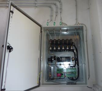
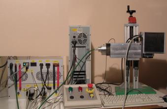
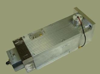
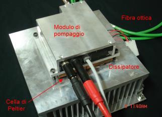
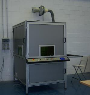
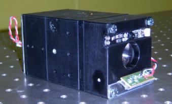
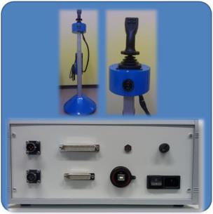
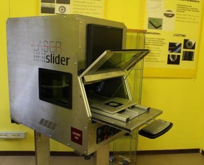
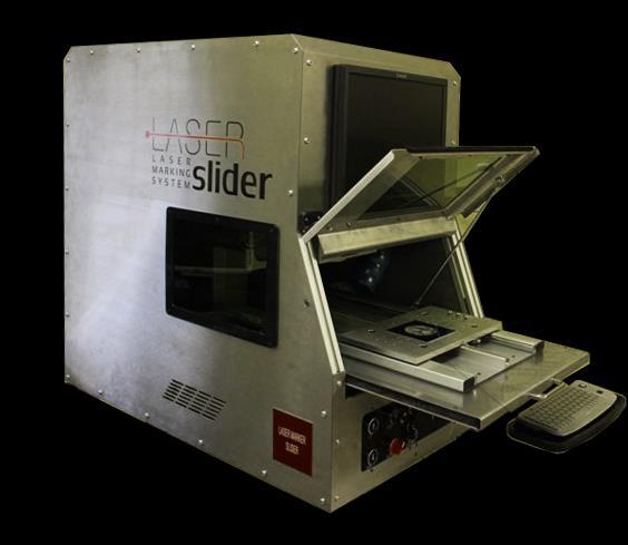
5 Focused product Portfolio LASER Systems Laser Processes development Laser Ready Fabrication of full custom Production machine: Laser Slider marking, drilling, cutting and welding Optical Design Beam shapers Fiber Pumping Simulation & prototyping Test set-up for processes engineering Electronics Design Laser s Power driver Automation Sensors Design, test and production Design of full custom electronics Hardware, Firmware and Software

6 Main Customers


7 LASER PROCESSES


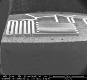
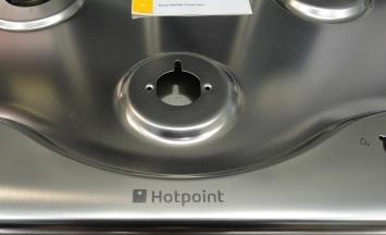
8 Micro Machining Microla knowledge is based on over 10 years of experience on specific materials such as: Polymers Metals Glasses Ceramics Leather Serial code, linear barcode, matrix code, QR code and logos can be engraved onto the surface of products Certified marking processes through engraving and ablation controlled thickness. Electronic Devices Gadget Carbon Fiber Organic Material Wood Silicon


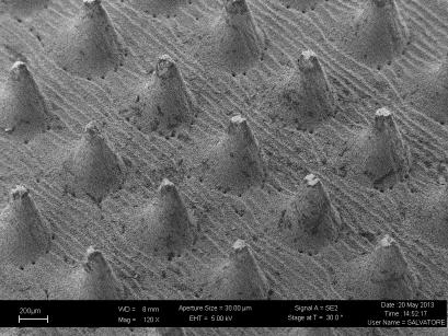
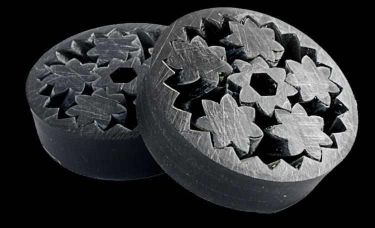
9 Micro Machining Soft and deep engraving processes for surface micro-machining used to create special pattern designed by customer Several application as microfluidic devices, heat transfer, chalcography and master for molding Micro holes and slits can be performed on request in micrometric range and related dimensional analysis is available


10 Micro Machining Soft and deep engraving processes for surface micro-machining used to create special pattern designed by customer Several application as microfluidic devices, heat transfer, chalcography and master for molding Micro holes and slits can be performed on request in micrometric range and related dimensional analysis is available

11 PRODUCTS

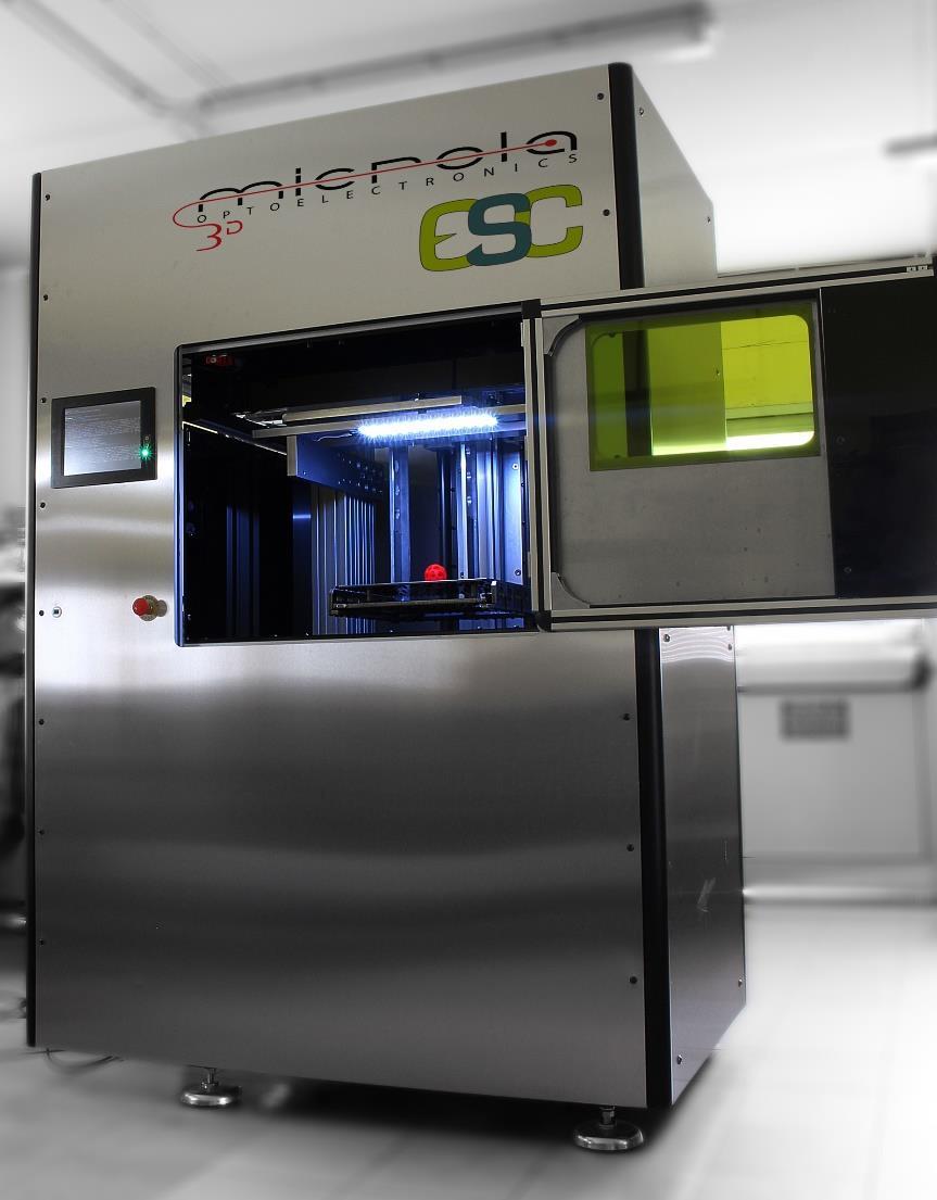
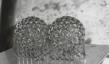
12 Micro Machining

13 Micro Machining

14 Micro Machining


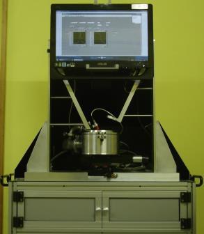
15 DESIGN OF LASER SYSTEMS


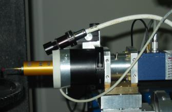
16 LASER welding LASER Plastic welding: Designing of Optical, Electronics and Soldering process Contour Welding Quasi-simultaneous welding Simultaneous welding Mask welding


17 LASER welding Microla designs laser systems for laser welding machines producers Optical systems design & Fabrication Electronics design & Fabrication Thermal heat sink design & Fabrication


18 LASER welding Microla design laser systems for laser welding machines producers Design Assembly


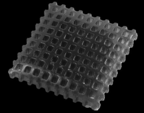

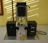
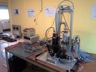
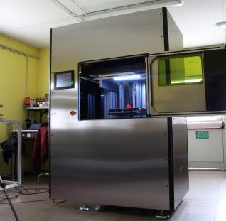
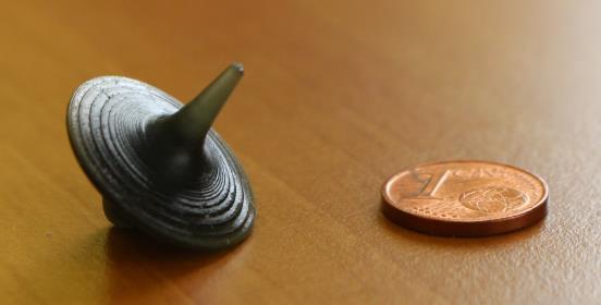
19 3D - Printing Forma: Polymeric Stereo-lithography LASER 1 cm 1 cm 1 cm 1 cm


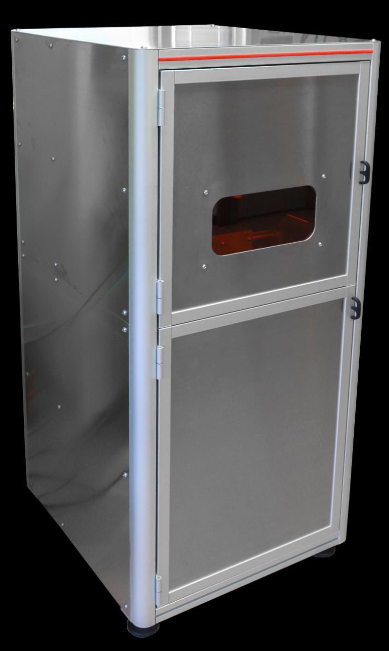
20 3D - Printing Microla s SLA Machine


21 4D - Printing 4D printing is: creating objects with advanced materials and innovative processes Self assembling structures Embedded optics Embedded electronics


22 4D - Printing 4D printing is: creating objects with advanced materials and innovative processes CONDUCTIVE POLYMERS FILM DEPOSITION IN STEREOLITHOGRAPHY

23 4D - Printing 4D printing is: creating objects with advanced materials and innovative processes Our nano-filler: carbon nanotubes length/diameter=10 4 external diameter= nm Other properties: High thermal conductivity High electrical conductivity Strong mechanical properties Carbon nanotubes Thermal conductivity [W/mK] Electrical conductivity [S/m] > Copper 400 6x10 7

24 4D - Printing Specific conductance(s/cm) 4D printing is: creating objects with advanced materials and innovative processes Results Resin without CNTs Wt% CNTs

25 4D - Printing 4D printing is: creating objects with advanced materials and innovative processes Stereolithography process


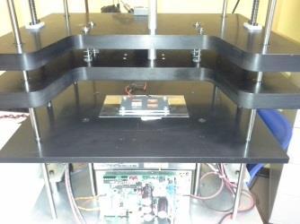
26 4D - Printing 4D printing is: creating objects with advanced materials and innovative processes Film deposition Platform Resin vat Resin IN Recoat er Resin vat Recoater Liquid resin Growing object Growing object

27 4D - Printing 4D printing is: creating objects with advanced materials and innovative processes Film deposition Advantages: Less material consumption The recoater holds minimum resin quantities The resin reservoir feeds directly the recoater Simple resin recovery at the end of process Accurate recoating Faster process

28 Future perspectives Finding optimal printing parameters Multi-material stereolithography Embedded micro/nano electronics with our printer and polymers! We will be on the market as soon as our 4D printer will be ready!


29 Thank you Felice Catania Microla Optoelectronics S.r.l. Tel: Fax: Labs & Administration Campus Tecnologico Località Baraggino CHIVASSO (TO)
Marking Cutting Welding Micro Machining Additive Manufacturing
 Marking Cutting Welding Micro Machining Additive Manufacturing Slide: 1 CM-F00003 Rev 4 G4 Pulsed Fiber Laser Slide: 2 CM-F00003 Rev 4 Versatility for Industry Automotive 2D/3D Cutting Night & Day Marking
CONTROL LASER TECHNOLOGY
 CONTROL LASER TECHNOLOGY CHANGING INDUSTRIES The Global Leader in Laser System Solutions for over 50 years specializing in: Laser Marking & Engraving, Laser Cutting, Micromachining, Semiconductors, Wire
Lasers for Materials Processing
 Lasers for Materials Processing Superior Reliability & Performance Any Material Any Pro cess At the forefront of materials processing applications Since its inception in 1966, Coherent has been at the
NanoFabrication Kingston. Seminar and Webinar January 31, 2017 Rob Knobel Associate Professor, Dept. of Physics Queen s University
 NanoFabrication Kingston Seminar and Webinar January 31, 2017 Rob Knobel Associate Professor, Dept. of Physics Queen s University What is NFK? It s a place, an team of experts and a service. The goal of
INTERNATIONAL ELECTRONIC CONFERENCE ON SENSORS AND APPLICATIONS
 INTERNATIONAL ELECTRONIC CONFERENCE ON SENSORS AND APPLICATIONS 01 16 JUNE 2014 AUTHORS / RESEARCHERS A.F.M. Anuar, Y. Wahab, H. Fazmir, M. Najmi, S. Johari, M. Mazalan, N.I.M. Nor, M.K. Md Arshad Advanced
Practical Applications of Laser Technology for Semiconductor Electronics
 Practical Applications of Laser Technology for Semiconductor Electronics MOPA Single Pass Nanosecond Laser Applications for Semiconductor / Solar / MEMS & General Manufacturing Mark Brodsky US Application
FIBER LASERS Ytterbium, Thulium and Erbium short pulse and CW lasers
 About V-Gen V-Gen develops, manufactures and markets high quality innovative laser systems for a wide range of industrial applications. The company s laser systems are the product of extensive experience
Applications of Maskless Lithography for the Production of Large Area Substrates Using the SF-100 ELITE. Jay Sasserath, PhD
 Applications of Maskless Lithography for the Production of Large Area Substrates Using the SF-100 ELITE Executive Summary Jay Sasserath, PhD Intelligent Micro Patterning LLC St. Petersburg, Florida Processing
Studying the Effect of Using Assist Gas with Low Power CO 2 LaserGlass Drilling
 American Journal of Engineering Research (AJER) 2018 American Journal of Engineering Research (AJER) e-issn: 2320-0847 p-issn : 2320-0936 Volume-7, Issue-1, pp-23-27 www.ajer.org Research Paper Open Access
Snapshot Mask-less fabrication of embedded monolithic SU-8 microstructures with arbitrary topologies
 Snapshot Mask-less fabrication of embedded monolithic SU-8 microstructures with arbitrary topologies Pakorn Preechaburana and Daniel Filippini Linköping University Post Print N.B.: When citing this work,
Design Analysis Process
 Prototype Design Analysis Process Rapid Prototyping What is rapid prototyping? A process that generates physical objects directly from geometric data without traditional tools Rapid Prototyping What is
Please contact T E L : ~ 4.
 Please contact T E L : +82-32-623-6320~ 4 E-MAIL : sales@kortherm.co.kr jshuh@kortherm.co.kr 1. LASER SAMPLE TEST - To serve companies and individuals who need sample tests before buying new laser micromachining
Advances in Laser Micro-machining for Wafer Probing and Trimming
 Advances in Laser Micro-machining for Wafer Probing and Trimming M.R.H. Knowles, A.I.Bell, G. Rutterford & A. Webb Oxford Lasers June 10, 2002 Oxford Lasers June 2002 1 Introduction to Laser Micro-machining
Introduction to Laser Material Processing
 Introduction to Laser Processing Laser material processing utilizes laser energy to modify the shape or appearance of a material. This method of material modification provides numerous advantages to customers
Application Bulletin 240
 Application Bulletin 240 Design Consideration CUSTOM CAPABILITIES Standard PC board fabrication flexibility allows for various component orientations, mounting features, and interconnect schemes. The starting
The Laser Processing of Diamond and Sapphire
 The Laser Processing of Diamond and Sapphire Neil Sykes Micronanics Limited neil@micronanics.com Diamond Diamond has the highest hardness and thermal conductivity of any bulk material 10/10 on the Mohs
EE 143 Microfabrication Technology Fall 2014
 EE 143 Microfabrication Technology Fall 2014 Prof. Clark T.-C. Nguyen Dept. of Electrical Engineering & Computer Sciences University of California at Berkeley Berkeley, CA 94720 EE 143: Microfabrication
Beam Shaping and Simultaneous Exposure by Diffractive Optical Element in Laser Plastic Welding
 Beam Shaping and Simultaneous Exposure by Diffractive Optical Element in Laser Plastic Welding AKL`12 9th May 2012 Dr. Daniel Vogler Page 1 Motivation: Quality and flexibility diffractive spot shaping
Micron Laser Technology
 Micron Laser Technology AS9100C / ISO9001:2008 Certified 18,000 sq. ft. facility with 20 laser drilling systems solely dedicated to microvia drilling, laser material processing, micromachining, prototyping,
Classification of Metal Removal Processes and Machine tools. Introduction to Manufacturing and Machining
 Classification of Metal Removal Processes and Machine tools Introduction to Manufacturing and Machining Production Engineering covers two domains: (a) Production or Manufacturing Processes (b) Production
NON-TRADITIONAL MACHINING PROCESSES ULTRASONIC, ELECTRO-DISCHARGE MACHINING (EDM), ELECTRO-CHEMICAL MACHINING (ECM)
, ELECTRO-CHEMICAL MACHINING (ECM)") NON-TRADITIONAL MACHINING PROCESSES ULTRASONIC, ELECTRO-DISCHARGE MACHINING (EDM), ELECTRO-CHEMICAL MACHINING (ECM) A machining process is called non-traditional if its material removal mechanism is basically
NON-TRADITIONAL MACHINING PROCESSES ULTRASONIC, ELECTRO-DISCHARGE MACHINING (EDM), ELECTRO-CHEMICAL MACHINING (ECM) A machining process is called non-traditional if its material removal mechanism is basically
Laser MicroJet Technology. Cool Laser Machining.
 Laser MicroJet Technology Cool Laser Machining www.synova.ch Synova S.A., headquartered in Duillier, Switzerland, manufactures leading-edge laser cutting systems since 1997 that incorporate the proprietary
Reviewed, accepted August 29, 2003
 ON CERAMIC PARTS FABRICATED RAPID PROTOTYPING MACHINE BASED ON CERAMIC LASER FUSION H. H. Tang*, H. C. Yen*, and W. H. Lin** *Department of Mechanical Engineering, National Taipei University of Technology,
ON-DEMAND PARTS MANUFACTURING. Quickparts
 ON-DEMAND PARTS MANUFACTURING Quickparts On-demand parts manufacturing services Using our additive and traditional manufacturing technologies, bring your design to life and create real functional end-use
Laser-induced transfer of PVD-films
 Laser-induced transfer of PVD-films Laser Transfer ARA-LT and ARA Authentic-LT PVD films are applied directly from the carrier foil to the product surface by using a laser beam. The ARA-LT and ARA Authentic-LT
Measurement of Microscopic Three-dimensional Profiles with High Accuracy and Simple Operation
 238 Hitachi Review Vol. 65 (2016), No. 7 Featured Articles Measurement of Microscopic Three-dimensional Profiles with High Accuracy and Simple Operation AFM5500M Scanning Probe Microscope Satoshi Hasumura
HOT LIGHT POWER TOOLS FROM THE JEWELRY ENGRAVING EXPERTS
 LASER MARKING, ENGRAVING & CUTTING SOLUTIONS HOT LIGHT POWER TOOLS FROM THE JEWELRY ENGRAVING EXPERTS LASER MARKING & ENGRAVING APPLICATIONS Precious Metals Novelty Items LASER MARKING & ENGRAVING SYSTEMS
PROCEEDINGS OF SPIE. Opportunities and challenges for 3D printing of solid-state lighting systems
 PROCEEDINGS OF SPIE SPIEDigitalLibrary.org/conference-proceedings-of-spie Opportunities and challenges for 3D printing of solid-state lighting systems Nadarajah Narendran Indika U. Perera Xi Mou Dinusha
FRAUNHOFER INSTITUTE FOR PHOTONIC MICROSYSTEMS IPMS. Application Area. Quality of Life
 FRAUNHOFER INSTITUTE FOR PHOTONIC MICROSYSTEMS IPMS Application Area Quality of Life Overlay image of visible spectral range (VIS) and thermal infrared range (LWIR). Quality of Life With extensive experience
The Swiss Army Knife for the Lab Micro Material Processing with the LPKF ProtoLaser U4
 The Swiss Army Knife for the Lab Micro Material Processing with the LPKF ProtoLaser U4 Micro Machining in the Lab LPKF ProtoLasers have been in use in leading electronics laboratories around the world
Virtual Manufacturing Laboratory:
 Virtual Manufacturing Laboratory: Desktop PC (Core i5)-3 nos. Software: 1. IGRIP Interactive Graphics Robot Instruction Programme. (Stratasys, Model-Objet. 30) 2. QUEST- Queuing vent Simulation (Deneb
Part 5-1: Lithography
 Part 5-1: Lithography Yao-Joe Yang 1 Pattern Transfer (Patterning) Types of lithography systems: Optical X-ray electron beam writer (non-traditional, no masks) Two-dimensional pattern transfer: limited
Energy & Space. International Presentations
 Energy & Space International Presentations 2012-2013 Advanced Electronics 3D Printed Circuit Boards 3D Printed Circuit Boards for Solder-Free Printable Electronics 4x4 Vehicles Arduino WiFi Android Controllers
Nanoimprinting of micro-optical components fabricated using stamps made with Proton Beam Writing
 Nanoimprinting of micro-optical components fabricated using stamps made with Proton Beam Writing JA van Kan 1 AA Bettiol 1,T. Osipowicz 2 and F. Watt 3 1 Research fellow, 2 Deputy Director of CIBA and
R&D, Project Management and Consulting
 R&D, Project Management and Consulting Catalogue Version 2 10-2018 Contents Specification of Pusher Fingers... 2 Sample case: Pusher Fingers specification... 3 Accessories... 3 Contact materials... 5 Overview
Major Fabrication Steps in MOS Process Flow
 Major Fabrication Steps in MOS Process Flow UV light Mask oxygen Silicon dioxide photoresist exposed photoresist oxide Silicon substrate Oxidation (Field oxide) Photoresist Coating Mask-Wafer Alignment
ESCC2006 European Supply Chain Convention
 ESCC2006 European Supply Chain Convention PCB Paper 20 Laser Technology for cutting FPC s and PCB s Mark Hüske, Innovation Manager, LPKF Laser & Electronics AG, Germany Laser Technology for cutting FPCs
Fieldlab Multi-material 3D Printing 3D printed structural electronics at TNO AMSYSTEMS Center
 Fieldlab Multi-material 3D Printing 3D printed structural electronics at TNO AMSYSTEMS Center Dr. Wijnand Germs wijnand.germs@tno.nl 3DP STRUCTURAL ELECTRONICS DEMO STATUS TODAY 3DP STRUCTURAL ELECTRONICS
Fabrication of suspended micro-structures using diffsuser lithography on negative photoresist
 Journal of Mechanical Science and Technology 22 (2008) 1765~1771 Journal of Mechanical Science and Technology www.springerlink.com/content/1738-494x DOI 10.1007/s12206-008-0601-8 Fabrication of suspended
Introduction to Manufacturing Processes
 Introduction to Manufacturing Processes Products and Manufacturing Product Creation Cycle Design Material Selection Process Selection Manufacture Inspection Feedback Typical product cost breakdown Manufacturing
Zukunftstechnologie Dünnglasbasierte elektrooptische. Research Center of Microperipheric Technologies
 Zukunftstechnologie Dünnglasbasierte elektrooptische Baugruppenträger Dr. Henning Schröder Fraunhofer IZM, Berlin, Germany Today/Overview Motivation: external roadmaps High Bandwidth and Channel Density
Outline. 1 Introduction. 2 Basic IC fabrication processes. 3 Fabrication techniques for MEMS. 4 Applications. 5 Mechanics issues on MEMS MDL NTHU
 Outline 1 Introduction 2 Basic IC fabrication processes 3 Fabrication techniques for MEMS 4 Applications 5 Mechanics issues on MEMS 2.2 Lithography Reading: Runyan Chap. 5, or 莊達人 Chap. 7, or Wolf and
THE EFFECTS OF MINITUARISATION OF PROJECTION STEREOLITHOGRAPHY EQUIPMENT ON PRINTING QUALITY
 9th International DAAAM Baltic Conference "INDUSTRIAL ENGINEERING 24-26 April 2014, Tallinn, Estonia THE EFFECTS OF MINITUARISATION OF PROJECTION STEREOLITHOGRAPHY EQUIPMENT ON PRINTING QUALITY Rayat,
The Department of Advanced Materials Engineering. Materials and Processes in Polymeric Microelectronics
 The Department of Advanced Materials Engineering Materials and Processes in Polymeric Microelectronics 1 Outline Materials and Processes in Polymeric Microelectronics Polymeric Microelectronics Process
DTU DANCHIP an open access micro/nanofabrication facility bridging academic research and small scale production
 DTU DANCHIP an open access micro/nanofabrication facility bridging academic research and small scale production DTU Danchip National Center for Micro- and Nanofabrication DTU Danchip DTU Danchip is Denmark
Greater accuracy and productivity through powerful new technology
 Greater accuracy and productivity through powerful new technology BUILDING ON A TRADITION OF EXCELLENCE With many recent advances in software and hardware, jig grinding continues to play a critical role
Solder Dross & Metal Recovery. High Performance Solder Products. High Precision Laser Cut Parts. Advanced Stencil & Laser Technology
 High Performance Solder Products Advanced Stencil & Laser Technology High Precision Laser Cut Parts Solder Dross & Metal Recovery Leaders in lead free technology SN100C North America Licensee of Nihon
Integrated Diode Laser System DioPower
 Integrated Diode Laser System DioPower PC with LETSoft program DioPower Integrated Components Applications Laser Diode from 15 to 120W Material processing Laser Diode driver up to 6V / 100A Laser soldering
COHERENT BEAM COMBINING OF HIGH POWER LASERS FOR MATERIALS PROCESSING
 COHERENT BEAM COMBINING OF HIGH POWER LASERS FOR MATERIALS PROCESSING www.civan.co.il EXECUTIVE SUMMARY Civan Advanced Technologies develops and manufactures single-mode, highpower laser systems with a
Stereolithography System Using Multiple Spot Exposure
 Stereolithography System Using Multiple Spot Exposure Yoji MARUTANI, Takayuki KAMITANI Faculty of Engineering OSAKA SANGYO UNIVERSITY 3-1-1 Nakagaito, Daito City OSAKA, 574 JAPAN ABSTRACT A new method
Figure 7 Dynamic range expansion of Shack- Hartmann sensor using a spatial-light modulator
 Figure 4 Advantage of having smaller focal spot on CCD with super-fine pixels: Larger focal point compromises the sensitivity, spatial resolution, and accuracy. Figure 1 Typical microlens array for Shack-Hartmann
Micro-PackS, Technology Platform. Security Characterization Lab Opening
 September, 30 th 2008 Micro-PackS, Technology Platform Security Characterization Lab Opening Members : Micro-PackS in SCS cluster From Silicium to innovative & commucating device R&D structure, gathering
Trans-African Hydro-Meteorological Observatory
 Trans-African Hydro-Meteorological Observatory Sensor Design Competition A design by: 1. Kolyanga Emmanuel Email: emmakoly@gmail.com 2. Wogisha Benjamin Email: wogisha@gmail.com Executive Summary Proposal
1.8.3 Haptic-Based CAD 1.9 About this Book 1.10 Exercises References Development of Additive Manufacturing Technology
 Contents 1 Introduction and Basic Principles 1 1.1 What Is Additive Manufacturing? 1 1.2 What Are AM Parts Used for? 3 1.3 The Generic AM Process 4 1.3.1 Step 1: CAD 4 1.3.2 Step 2: Conversion to STL 4
AgilOptics mirrors increase coupling efficiency into a 4 µm diameter fiber by 750%.
 Application Note AN004: Fiber Coupling Improvement Introduction AgilOptics mirrors increase coupling efficiency into a 4 µm diameter fiber by 750%. Industrial lasers used for cutting, welding, drilling,
Laser Engraving. Exotica Crafts Hotel Supply and Custom Products
 SALES KIT LOGO 1 Laser Engraving Laser Engraving or also known as laser etching is the process of burning the surface of material with a focused laser to engrave or etch your desired graphic or logo. A
Diverse Lasers Support Key Microelectronic Packaging Tasks
 Diverse Lasers Support Key Microelectronic Packaging Tasks Written by D Muller, R Patzel, G Oulundsen, H Halou, E Rea 23 July 2018 To support more sophisticated and compact tablets, phones, watches and
Machine Tool Order Intake in Germany Real changes against the previous year in %
 Brilliant Performance Efficiency, Power, Brightness, Reliability of nlight Diode Laser Systems Kirk, Rob, Frank, Ingolf, others? Current economic situation: (might skip as total debrief) We are in the
DTU DANCHIP an open access micro/nanofabrication facility bridging academic research and small scale production
 DTU DANCHIP an open access micro/nanofabrication facility bridging academic research and small scale production DTU Danchip National Center for Micro- and Nanofabrication DTU Danchip DTU Danchip is Denmark
CAPABILITIES Rev novembre 2017
 THE PRINTED CIRCUIT BOARD PRODUCTION PROCESS CAPABILITIES Rev. 8-27 novembre 2017 Tecnometal Srl PCB & ELECTRONICS INDUSTRY SERVICES TECNOMETAL S.r.l. Via Ancona nr. 3-20060 Trezzano Rosa (MI) ITALY Tel:
Novel laser power sensor improves process control
 Novel laser power sensor improves process control A dramatic technological advancement from Coherent has yielded a completely new type of fast response power detector. The high response speed is particularly
Здра вствуйте, това рищи!
 Manufacturing of Smart Objects by Printing Technologies Здра вствуйте, това рищи! Moscow / RUS, June 05, 2013 Reinhard R. Baumann Chemnitz University of Technology Chair of Digital Printing Fraunhofer
ADVANCES IN USING A POLYMERIC TAPE FOR LASER-INDUCED DEPOSITION AND ABLATION
 ADVANCES IN USING A POLYMERIC TAPE FOR LASER-INDUCED DEPOSITION AND ABLATION Arne Koops, tesa AG, Hamburg, Germany Sven Reiter, tesa AG, Hamburg, Germany 1. Abstract Laser systems for industrial materials
flexible lighting technology
 As a provider of lighting solutions for the Machine Vision Industry, we are passionate about exceeding our customers expectations. As such, our ISO 9001 quality procedures are at the core of everything
DOE Project: Resist Characterization
 DOE Project: Resist Characterization GOAL To achieve high resolution and adequate throughput, a photoresist must possess relatively high contrast and sensitivity to exposing radiation. The objective of
Scanning solutions for industrial applications
 Scanning solutions for industrial applications Competence made in Germany ARGES has been a pioneer in the laser sector for over 20 years. In addition to the production and development of a versatile applicable
Low Temperature Integration of Thin Films and Devices for Flexible and Stretchable Electronics
 Low Temperature Integration of Thin Films and Devices for Flexible and Stretchable Electronics Pooran Joshi, Stephen Killough, and Teja Kuruganti Oak Ridge National Laboratory FIIW 2015 Displays and PV
MICROSTRUCTURING OF METALLIC LAYERS FOR SENSOR APPLICATIONS
 MICROSTRUCTURING OF METALLIC LAYERS FOR SENSOR APPLICATIONS Vladimír KOLAŘÍK, Stanislav KRÁTKÝ, Michal URBÁNEK, Milan MATĚJKA, Jana CHLUMSKÁ, Miroslav HORÁČEK, Institute of Scientific Instruments of the
A new class of LC-resonator for micro-magnetic sensor application
 Journal of Magnetism and Magnetic Materials 34 (26) 117 121 www.elsevier.com/locate/jmmm A new class of LC-resonator for micro-magnetic sensor application Yong-Seok Kim a, Seong-Cho Yu a, Jeong-Bong Lee
Backplane Considerations for an RGB 3D Display Device
 by Daniel Browning, 7.10.14.v.1 0. Introduction This is the third paper in a series that describes a futuristic design for a 3D display device. The first paper introduced the subject and looked at invisibility
THE ARCOR WAY: A PASSION FOR PRECISION
 THE ARCOR WAY: A PASSION FOR PRECISION 1 THE A-TEAM Our entire team is ready to take on your toughest challenges. When you work with our A-Team leaders, you can feel confident that From engineers to project
Department of 4i Laboratory IITKanpur. Conventional/non conventional Machining tools For industrial applications
 Department of 4i Laboratory IITKanpur Conventional/non conventional Machining tools For industrial applications Machining facilities available Rapid prototyping CNC Water Jet Laser cutting Lathe Drilling
Nanoimprint lithography with a focused laser beam for the fabrication of micro-/nano-hybrid patterns
 Supplementary Material (ESI) for Lab on a Chip This journal is The Royal Society of Chemistry 20XX Nanoimprint lithography with a focused laser beam for the fabrication of micro-/nano-hybrid patterns Hyungjun
Laser patterning and projection lithography
 Introduction to Nanofabrication Techniques: Laser patterning and projection lithography Benjamin Johnston Macquarie University David O Connor Bandwidth Foundry - USYD The OptoFab node of ANFF Broad ranging
LASER MARKING SYSTEM MOD. ALS 6100
 LASER MARKING SYSTEM MOD. ALS 6100 Aurel Automation SpA Via Foro dei Tigli, 4 47015 MODIGLIANA (FC) ITALY Tel. +39 0546 941124 Fax +39 0546 941660 www.aurelautomation.com automation@aurelautomation.com
Laser Experts in Semiconductor Manufacturing
 Laser Experts in Semiconductor Manufacturing Backed by more than three decades of experience in laser material processing, ROFIN is one of the best established companies in this field. The company has
Photonic device package design, assembly and encapsulation.
 Photonic device package design, assembly and encapsulation. Abstract. A.Bos, E. Boschman Advanced Packaging Center. Duiven, The Netherlands Photonic devices like Optical transceivers, Solar cells, LED
MICRO-ENGINEERING APPLICATIONS OF PULSED LASERS
 MICRO-ENGINEERING APPLICATIONS OF PULSED LASERS Nadeem Rizvi Exitech Limited Hanborough Park, Long Hanborough, Oxford OX8 8LH, United Kingdom. INTRODUCTION Lasers are currently being used world-wide in
Sealed CO 2 DIAMOND. Sealed CO 2 Laser Systems. Reliable Lasers for Precision Machining
 Coherent Sealed CO 2 RF-Excited DIAMOND Sealed CO 2 Laser Systems Reliable Lasers for Precision Machining Brilliance DIAMOND K-Series and G-Series lasers feature Brilliance, a combination of mode quality,
Since
 Since 1999 www.kortherm.co.kr Advanced Laserr Technology at KORTherm Science S Since founded in 1999 we put our endeavor into building a specialized business, focusing on the application of lasers and
Lockheed Martin 2016 LOCKHEED MARTIN CORPORATION. ALL RIGHTS RESERVED
 Lockheed Martin 1 Helping the Future Arrive 2 Our People 115,000 Employees 60,000 Scientists & Engineers 500+ U.S. Facilities Operating in 70 Countries 3 Lockheed Martin 100+ Years of Accelerating Tomorrow
Packaging Roadmap: The impact of miniaturization. Bob Pfahl, inemi Celestica-iNEMI Technology Forum May 15, 2007
 Packaging Roadmap: The impact of miniaturization Bob Pfahl, inemi Celestica-iNEMI Technology Forum May 15, 2007 The Challenges for the Next Decade Addressing the consumer experience using the converged
Visual Imaging in the Electronic Age
 Visual Imaging in the Electronic Age ART 2107, ARCH 3702, CS 1620, ENGRI 1620 3D Printing October 20, 2015 Prof. Donald P. Greenberg dpg5@cornell.edu Types of 3D Printers Selective deposition printers
Nanofabrication technologies: high-throughput for tomorrow s metadevices
 Nanofabrication technologies: high-throughput for tomorrow s metadevices Rob Eason Ben Mills, Matthias Feinaugle, Dan Heath, David Banks, Collin Sones, James Grant-Jacob, Ioannis Katis. Fabrication fundamentals
A BASIC EXPERIMENTAL STUDY OF CAST FILM EXTRUSION PROCESS FOR FABRICATION OF PLASTIC MICROLENS ARRAY DEVICE
 A BASIC EXPERIMENTAL STUDY OF CAST FILM EXTRUSION PROCESS FOR FABRICATION OF PLASTIC MICROLENS ARRAY DEVICE Chih-Yuan Chang and Yi-Min Hsieh and Xuan-Hao Hsu Department of Mold and Die Engineering, National
Midaz Micro-Slab DPSS Lasers:
 Midaz Micro-Slab DPSS Lasers: Higher power & pulse rate for higher speed micromachining Professor Mike Damzen Midaz Laser Ltd 4 June 2008 AILU Meeting Industrial opportunities in laser micro and nano processing
Ch 2: Manufacturing Operations
 Ch 2: Manufacturing Operations Learning Objectives: By the end of the lecture the student should be able to: Explain the difference between technological and economical definition of manufacturing. Properly
Consortium Capabilities
 Consortium Capabilities The driver in advanced materials development is to create products with competitive advantages. Products must continuously become faster, lighter and cheaper and must provide additional
GROMAX - HAN S LASER MARKER SERIES For
 more detailed information, please visit our website at GROMAX - HAN S LASER MARKER SERIES For www.gromaxonline.com Fiber Series Laser engraving/marking is the process of using lasers to engrave or etch
Weber Manufacturing Technologies Kitchen & Bath
 Weber Manufacturing Technologies Kitchen & Bath Chris Barber Overview Founded in 1962, Weber Manufacturing Technologies Inc. is a leading manufacturer of precision tooling for Automotive, Aerospace, and
INDUSTRIAL TECHNOLOGIES FOR SCHOOLS
 INDUSTRIAL TECHNOLOGIES FOR SCHOOLS (LMS) Director: Prof. George Chryssolouris Dept. of Mechanical Engineering & Aeronautics University of Patras, Greece INDUSTRIAL TECHNOLOGIES FOR SCHOOLS: BACKGROUND
Highly Versatile Laser System for the Production of Printed Circuit Boards
 When batch sizes go down and delivery schedules are tight, flexibility becomes more important than throughput Highly Versatile Laser System for the Production of Printed Circuit Boards By Bernd Lange and
Nanostencil Lithography and Nanoelectronic Applications
 Microsystems Laboratory Nanostencil Lithography and Nanoelectronic Applications Oscar Vazquez, Marc van den Boogaart, Dr. Lianne Doeswijk, Prof. Juergen Brugger, LMIS1 Dr. Chan Woo Park, Visiting Professor
Shiga Prefecture. Group of specialists challenging the impossible and creating unique products. Developing and producing original LCD systems
 I.S.T. Corporation (Otsu City) Group of specialists challenging the impossible and creating unique products Mold Research Co., Ltd. (Kusatsu City) Producing high precision parts by powder injection molding
True Three-Dimensional Interconnections
 True Three-Dimensional Interconnections Satoshi Yamamoto, 1 Hiroyuki Wakioka, 1 Osamu Nukaga, 1 Takanao Suzuki, 2 and Tatsuo Suemasu 1 As one of the next-generation through-hole interconnection (THI) technologies,
Optical Bus for Intra and Inter-chip Optical Interconnects
 Optical Bus for Intra and Inter-chip Optical Interconnects Xiaolong Wang Omega Optics Inc., Austin, TX Ray T. Chen University of Texas at Austin, Austin, TX Outline Perspective of Optical Backplane Bus
Unique and sustainable surface refinement of products with innovative thin films: Ara Authentic. R. Domnick, Ara-Authentic GmbH
 Unique and sustainable surface refinement of products with innovative thin films: Ara Authentic R. Domnick, Ara-Authentic GmbH 1 Introduction - About us - Piracy of products a growing problem - Protection
WDM board-level optical communications
 MIT Microphotonics Center Spring Meeting, May 22 nd WDM board-level optical communications Jürgen Schrage Siemens AG,, Germany Outline Introduction to board-level optical communications, WDM motivation
64 Channel Flip-Chip Mounted Selectively Oxidized GaAs VCSEL Array
 64 Channel Flip-Chip Mounted Selectively Oxidized GaAs VCSEL Array 69 64 Channel Flip-Chip Mounted Selectively Oxidized GaAs VCSEL Array Roland Jäger and Christian Jung We have designed and fabricated
3D and Aerosol Printed Conductor Dielectric Full- 3D RF Metamaterials
 3D and Aerosol Printed Conductor Dielectric Full- 3D RF Metamaterials June 22, 2017 Jimmy Hester, Evan Nguyen, Jesse Tice, and Vesna Radisic Approved for Public Release: NG17-1180, 6/2/17 Outline Introduction