Please contact T E L : ~ 4.
|
|
|
- Abraham Richard
- 5 years ago
- Views:
Transcription

1 Please contact T E L : ~ 4 sales@kortherm.co.kr jshuh@kortherm.co.kr
2 1. LASER SAMPLE TEST - To serve companies and individuals who need sample tests before buying new laser micromachining systems, KORTherm Science provides laser testing with a wide range of lasers. For quotations, following rules will be applied in the contract Minimum working time in a contract : 10 hours (based on 5 years of experience worker) Testing is performed by the drawing that customer provides. Labor Charges 1) UV,GREEN,IR LASER : $150/hour *10hours = $1,500 2) CO2 LASER : $200/hour * 10hours = $2,000 Minimum 4 hours required for Laser Settings: alignment and parameter. Labor charge varied by the difficulty of testing Additional tools and parts not included and to be quoted seperately. Test result not guaranteed once agreed
 2 Quotation 3 Test request form to be filled out and")
 6 Test Sample to return to the customer (by")
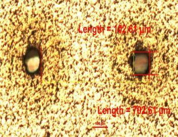
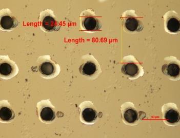
3 1-1. Process of LASER SAMPLE TEST 1 Technical request from customer (Feasibility and test details to be specified : Laser type, thickness, materials) 2 Quotation 3 Test request form to be filled out and samples to be sent by customer 7 Payment in advance KORTHERM 4 LASER Test done 5 Test report to share through (Microscope image and analysis included) 6 Test Sample to return to the customer (by Express) CUSTOMER
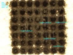
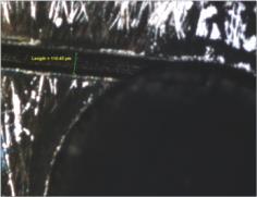
4 1-2. What are Parameters for laser processing? 1. Pass 2. Scanning Speed 3. Pulse Energy 4. Pulse Width 5. Repetition Rate Depending on the sample status and processing, KOS optimizes Laser procssing parameters to find out the best processing conditions. 4
5 1-2.
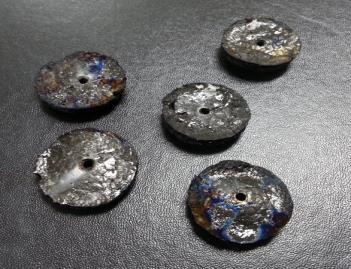
6 2. SAMPLE TEST Cutting Hole Drilling ITO / FTO Patterning Scribing Marking Film Cutting (Polymer) Transparent materials such as Glass, Quartz, Sapphire, Fused Silica(CaF 2, MgF 2 ) ITO/PI, ITO/PET, ZnO/PI, ZnO/PET Carbon, Graphene

7 3. SAMPLE TEST TOOL


8 3. SAMPLE TEST TOOL-1 µ-lab Microscope/Scanner NIR radiation : 1064 nm Precisely small beam control Compact size design Easy to use with a software Up to 20W average output power More than 20kW peak power Works in true CW or pulsed regime Applications - Marking - Engraving - Soldering - Micromachining - Cutting - Micro hole drilling - Scribing - Sintering - Welding -Thin film patterning - Edge isolation of solar cell


9 3. SAMPLE TEST TOOL-2 µ-fab Micromachining System Single Nd:YAG Laser 1064/532/355nm wavelength Scribing speed: mm/s Scribing width < 60um Vacuum chuck system Assist gas and Suction system Auto alignment and inspection system Applications - Marking - Engraving - Soldering - Micromachining - Cutting - Micro hole drilling - Scribing - Sintering - Welding - Thin film patterning - Edge isolation of solar cell


10 4. SAMPLE TEST TOOL-3 Light from CO 2 lasers is absorbed strongly by most nonmetallic materials. This makes CO 2 lasers a natural choice for cutting a wide variety of organic and plastic materials. CO 2 lasers can cut materials of varying thickness-for example. from 0.05mm for ceramic to 30mm for wood. ABS,PET Cotton Polyethylene Acrylic Epoxy Resins Polyimide(Kapton T Alumina Leather Polyurethane Aluminum Nitride Maple PVC Birch Mylar TM Quartz Borosilicate Glass Nylon Rosewood Cardboard Paper Rubber Ceramic Plywood Silicon Corian TM PMMA Teflon TM M )
11 5. APPLICATIONS Photovoltaic Applications Thin Film Scribing P1, P2, P3 Edge Deletion P4 Photovoltaic Applications c-si Edge Isolation Doping / Diffusion Data-Matrix marking Metal Wrap Through Selective Emitter Semiconductor Dicing Via drilling Thin film ablation Microelectronic PCB cutting, drilling Depanelling Ceramic Cutting Engraving / cavity Drilling Polymer / Polyimide Cutting Drilling Texturing Metal Deep engraving / 3D Drilling Texturing Films Cutting Ablation Carbon - Graphene Cutting Drilling
12 6. LASER SPECIFICATION ND-YAG (DPSS) LASER - 355nm / 532nm / 1064nm CO2 LASER μm / 9.35μm / 9.4μm FIBER LASER nm EXCIMER LASER - 193nm / 248nm


 Wavelength:")
 Wavelength:")

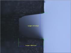
13 7. Laibray Polymer (1) Cutting of polymer Wavelength: 1064nm Pulse energy: Rep rate: 40kHz Proceeding speed : 300mm/s Hole Drilling (on the PI film) Scribing of IMI film on Glass Pulse energy: Rep rate: 30kHz Proceeding speed : 500mm/s Film Release FTO Patterning (FTO on glass) Wavelength: 1060nm FTO Patterning (on the PI film) Wavelength: 1080nm PET Film Cutting Wavelength: 10.6 μm PET Easy Cut ITO Patterning (on the PET film)
 PET")

")


14 7. Library Polymer (2) PET Film Cutting PET Film Cutting FTO Release (FTO on glass) Polyimide Film Release Polyimide Film Cutting ITO Scribing (Including Ag) ABS Hole Drilling Thickness: 2.8mm Polaroid Film Patterning ITO Scribing (Ag Including)
 Acrylic Resin")


 PMMA")


15 7. Library Polymer (3) Acrylic Resin Patterning Wavelength: 10.6 μm Thickness: 5mm PI Film Drilling ITO Patterning Wavelength: 1,080nm (PICO Laser) PMMA Cutting Wavelength: 10.6 μm Ag Film Punching (Ag & Polymer Film) Wavelength: 10.6 μm PI Film Drilling FTO Scribing Polymer Deposition Thin-film Patterning ITO Scribing Wavelength: 1,080nm
 (1)")


16 7. Library Wafer (Ceramic) (1) Scribing of Ceramic Wavelength: 1080nm Solar cell Wafer Edge isolation Wavelength : 532nm Solar Cell Wafer Doping Wafer Doping Wavelength : 532nm Ceramic Film Patterning LED CELL Si Wafer Drilling Wavelength : 532nm Si Wafer Align Key Marking Ceramic Hole Wavelength: 10.6 μm
 Drilling of Si-Wafer")


17 7. Library Wafer (Si/Ceramic) (2) Drilling of Si-Wafer Wavelength: 1064nm Pulse energy: Rep rate: 10kHz Proceeding speed : 20mm/s Si Wafer Round Cutting Thickness: 520 μm Edge Isolation of Si Solarcell Wavelength: 1064nm Pulse energy: Rep rate: 500kHz Proceeding speed : 2m/s Si Wafer Pattern Cutting Removal of TCO on CIGS + Mo+Glass Wavelength: 1064nm Pulse energy: Rep rate: 500kHz Proceeding speed : 2m/s Removal of CIGS on Mo+Glass Wavelength: 1064nm Pulse energy: Rep rate: 500kHz Proceeding speed : 2m/s Silicone Sheet Hole Drilling AIN Wafer Hole Drilling Si Wafer Pattern Cutting
 (3)")


 Green")


 Si Wafer")
18 7. Library Wafer (Si/Ceramic) (3) Patterned Si-Wafer Cutting (Membrane Pattern) Si Wafer Full Cutting ARC Ablation (Anti-Reflective Coating) LGBC Scribing (Laser Grooved Buried Contracts) Green Sheet Scribing (Unfired Ceramic Sheet) Si Wafer Cutting Fired Ceramic Sheet (Via Hole) Si Wafer Patterning Si Wafer Scribing (Scanner Type)
 (4)")
")


19 7. Library Wafer (Si/Ceramic) (4) Ceramic Cutting (Ni Oxide + YSZ) Wavelength: 1064nm Ceramic Cutting (Ni Oxide + YSZ) Wavelength: 1064nm Si Wafer Round Cutting Si Wafer Hatching Patterning Si Wafer Full Cutting (Cross-Section) Thickness: 0.3mm Si Wafer Cutting (Membrane Pattern)
")


 Removing of")

20 7. Library Metal/Ferrite (1) Via Hole Metal on PET Wavelength: 10.6μm SUS Thin Film Hole Drilling Ferrite Compound Cutting (Cross-Section) Thickness: 150μm Metal Hole Drilling Cu Thin Film Drilling Scribing of ZnO on glass Mo Scribing (Solar Cell Thin Film) Removing of ZnO on Glass Pulse energy: Rep rate: 30kHz Proceeding speed : 200mm/s


 Aluminium")

21 7. Library Metal (2) Tungsten-Carbide Hole Drilling (Via Hole) Tungsten-Carbide & Nickel Complex Hole Drilling (Via Hole) Mg Surface Patterning Wafer Doping Wavelength : 532nm Tantalum (Ta) Hole Drilling Cu Wafer Cutting Gold Thin Film Patterning (Inner Transparent & Flexible PDMA Film) Aluminium Oxide Wafer Hole Drilling Mo (Molybdenum) Thin Film Hole Drilling
 SUS Scribing")
 Scribing")


 Ag")


22 7. Library Metal (3) SUS Scribing Invar Steel (Fe-NI) Scribing SUS420J2 Scribing Cathode/Anode Electrode Cutting (Copper & Aluminium) Thickness: 25μm Pure Mg Cutting (Magnesium) Ag Coated GdBCO on STS Cutting (Cross-Section) Aluminium Through Line Patterning Metal Oxide Film Ablation Si Wafer Metal Layer Ablation
 Au Pad Full")


 Ag")


23 7. Library Metal (4) Au Pad Full Scribing Copper Foil Hole Drilling Back Electrode Film Ablation (ZnO on the Glass) Ag Nano Wire Thin-film Scribing Wavelength: 1064nm Cu Hole Drilling Thickness: 0.1mm SUS Hole Drilling Thickness: 0.1mm Alumina Tube Hole Drilling Wavelength: 10.6μm Metal Film Patterning SUS304 Hole Drilling


24 7. Library Carbon/Glass/Diamond/Quartz. (1) Graphite Patterning Scribing of Glass Pulse energy: Rep rate: 30kHz Proceeding speed : 200mm/s Hole Drilling on the Aluminium Wavelength : 355nm Artificial Diamond Patterning Glass Patterning Quartz Patterning Graphene Cutting Carbon Disk Hole Drilling (100% Carbon) Quartz Hole Patterning (Via Hole)

")

")


")

25 7. Library Transparent materials. (2) Quartz Micro-Hole Drilling (Cross-Section) Sapphire Micro-Hole Drilling Thickness: 420μm Soda-Lime Glass Hole Scribing (Via Hole) Wavelength : 355nm Epoxy Resin Patterning Wavelength: 10.6μm Superconductor GdBCO Thin Film Scribing (Cross-Section) Superconductor GdBCO Thin Film Hole Drilling (Through Hole) Quartz Scribing Wavelength: 10.6μm Flexible Gorilla Glass Cutting Slide Glass Cutting

 Sapphire Wafer")
")

 Glass")

 Glass")


26 7. Library Transparent materials. (3) Sapphire Wafer Cutting (Cross-Section) Gold/Pt/CVD Diamond Pattern Scribing (Using Edge Alignment) Glass Full Cutting Thickness: 0.5T PMN-PT Patterning (Piezoelectric Element) Glass Microwire Cutting Quartz Thin Film Cutting Sapphire Wafer Scribing OLED Light Hole Drilling Thickness: 0.88mm Glass Channel Patterning (Lab-on-a-chip)


27 7. Library Transparent materials. (4) Quartz Wafer Hole Drilling Wavelength: 10.6μm Thickness: 500μm Quartz Wafer Round Cutting Wavelength: 10.6μm Thickness: 680μm Transparent Electrode Scribing Thickness: 0.71mm Glass Full Cutting


28 after the F-πShaper Input laser beam I Output beam I 1/e² 6mm p 6mm In Case of F-πShaper required, additional costs worth of 10 hours will be charged.
29 Thank you! KORTherm Science Co., Ltd. T E L : ~ 4 sales@kortherm.co.kr jshuh@kortherm.co.kr C-1203B, Woorim Lion s Valley 425, Cheoncheon-dong Bupyeong-gu, Incheon, South Korea
Since
 Since 1999 www.kortherm.co.kr Advanced Laserr Technology at KORTherm Science S Since founded in 1999 we put our endeavor into building a specialized business, focusing on the application of lasers and
Practical Applications of Laser Technology for Semiconductor Electronics
 Practical Applications of Laser Technology for Semiconductor Electronics MOPA Single Pass Nanosecond Laser Applications for Semiconductor / Solar / MEMS & General Manufacturing Mark Brodsky US Application
Marking Cutting Welding Micro Machining Additive Manufacturing
 Marking Cutting Welding Micro Machining Additive Manufacturing Slide: 1 CM-F00003 Rev 4 G4 Pulsed Fiber Laser Slide: 2 CM-F00003 Rev 4 Versatility for Industry Automotive 2D/3D Cutting Night & Day Marking
Precision Cold Ablation Material Processing using High-Power Picosecond Lasers
 Annual meeting Burgdorf Precision Cold Ablation Material Processing using High-Power Picosecond Lasers Dr. Kurt Weingarten kw@time-bandwidth.com 26 November 2009 Background of Time-Bandwidth Products First
Sub-ns Microchip Lasers Technology: Overview and Progress in Health Science and Industrial Applications Florent Thibault
 Sub-ns Microchip Lasers Technology: Overview and Progress in Health Science and Industrial Applications Florent Thibault May 2012/ page 1 Agenda 1. Company overview 2. Laser technology 3. Added value for
Midaz Micro-Slab DPSS Lasers:
 Midaz Micro-Slab DPSS Lasers: Higher power & pulse rate for higher speed micromachining Professor Mike Damzen Midaz Laser Ltd 4 June 2008 AILU Meeting Industrial opportunities in laser micro and nano processing
Application of EOlite Flexible Pulse Technology. Matt Rekow Yun Zhou Nicolas Falletto
 Application of EOlite Flexible Pulse Technology Matt Rekow Yun Zhou Nicolas Falletto 1 Topics Company Background What is a Flexible Pulse Laser? Why Tailored or Flexible Pulse? Application of Flexible
HipoCIGS: enamelled steel as substrate for thin film solar cells
 HipoCIGS: enamelled steel as substrate for thin film solar cells Lecturer D. Jacobs*, Author S. Efimenko, Co-author C. Schlegel *:PRINCE Belgium bvba, Pathoekeweg 116, 8000 Brugge, Belgium, djacobs@princecorp.com
LARGE SELECTION LASER MARKER. FAYb CO2. Laser Marker Selection Guide LASER MARKER LP-S/SW SERIES LP-300 SERIES LP-M/MA SERIES LP-V/W SERIES
 Laser Marker Selection Guide LARGE SELECTION LASER MARKER FAYb LASER MARKER LP-M/MA SERIES LP-Z SERIES LP-S/SW SERIES LP-RF SERIES LP-V/W SERIES CO2 LASER MARKER LP-RC SERIES LP-400 SERIES LP-GS SERIES
Excimer laser projector for microelectronics applications
 Excimer laser projector for microelectronics applications P T Rumsby and M C Gower Exitech Ltd Hanborough Park, Long Hanborough, Oxford OX8 8LH, England ABSTRACT Fully integrated excimer laser mask macro
Advances in Laser Micro-machining for Wafer Probing and Trimming
 Advances in Laser Micro-machining for Wafer Probing and Trimming M.R.H. Knowles, A.I.Bell, G. Rutterford & A. Webb Oxford Lasers June 10, 2002 Oxford Lasers June 2002 1 Introduction to Laser Micro-machining
Micron Laser Technology
 Micron Laser Technology AS9100C / ISO9001:2008 Certified 18,000 sq. ft. facility with 20 laser drilling systems solely dedicated to microvia drilling, laser material processing, micromachining, prototyping,
Studying the Effect of Using Assist Gas with Low Power CO 2 LaserGlass Drilling
 American Journal of Engineering Research (AJER) 2018 American Journal of Engineering Research (AJER) e-issn: 2320-0847 p-issn : 2320-0936 Volume-7, Issue-1, pp-23-27 www.ajer.org Research Paper Open Access
Laser MicroJet Technology. Cool Laser Machining.
 Laser MicroJet Technology Cool Laser Machining www.synova.ch Synova S.A., headquartered in Duillier, Switzerland, manufactures leading-edge laser cutting systems since 1997 that incorporate the proprietary
PRESENTATION OF METALLURGICAL SUPPLIES A METALLOGRAPHY WORLD CORPORATION POLISHING CLOTH'S
 PRESENTATION OF METALLURGICAL SUPPLIES A METALLOGRAPHY WORLD CORPORATION POLISHING CLOTH'S PREMIUM POLISHING CLOTH SAMPLE CARD AVAILABLE Quick reference guide cross compares to Struers & Buehler Cloth
Micro Precision Apertures
 National Aperture, Inc. Micro Precision Apertures Product Guide Precision apertures, targets and patterns, including round, slit, square, etc., for universal and high power applications National Aperture,
DLMP TECHNOLOGY CUTTING ENGRAVING MARKING. Creating Opportunities with Digital Laser Material Processing Technology
 DLMP TECHNOLOGY TM CUTTING ENGRAVING MARKING Creating Opportunities with Digital Laser Material Processing Technology DLMP (Digital Laser Material Processing) Technology DLMP technology enables users to
AVIA DPSS Lasers: Advanced Design for Increased Process Throughput
 White Paper AVIA DPSS Lasers: Advanced Design for Increased Process Throughput The Q-switched, diode-pumped, solid-state (DPSS) laser has become a widely employed tool in a broad range of industrial micromachining
FIBER LASERS Ytterbium, Thulium and Erbium short pulse and CW lasers
 About V-Gen V-Gen develops, manufactures and markets high quality innovative laser systems for a wide range of industrial applications. The company s laser systems are the product of extensive experience
Who we are. was born in 2006 as Spin-Off of Politecnico of Torino. Full time people employed 8. Laboratories and facilities 300 m 2
 Who we are was born in 2006 as Spin-Off of Politecnico of Torino Full time people employed 8 Laboratories and facilities 300 m 2 Administration and offices 250 m 2 Consolidated Turnover more then 600k
CHAPTER 11: Testing, Assembly, and Packaging
 Chapter 11 1 CHAPTER 11: Testing, Assembly, and Packaging The previous chapters focus on the fabrication of devices in silicon or the frontend technology. Hundreds of chips can be built on a single wafer,
Diverse Lasers Support Key Microelectronic Packaging Tasks
 Diverse Lasers Support Key Microelectronic Packaging Tasks Written by D Muller, R Patzel, G Oulundsen, H Halou, E Rea 23 July 2018 To support more sophisticated and compact tablets, phones, watches and
ESCC2006 European Supply Chain Convention
 ESCC2006 European Supply Chain Convention PCB Paper 20 Laser Technology for cutting FPC s and PCB s Mark Hüske, Innovation Manager, LPKF Laser & Electronics AG, Germany Laser Technology for cutting FPCs
NON-TRADITIONAL MACHINING PROCESSES ULTRASONIC, ELECTRO-DISCHARGE MACHINING (EDM), ELECTRO-CHEMICAL MACHINING (ECM)
, ELECTRO-CHEMICAL MACHINING (ECM)") NON-TRADITIONAL MACHINING PROCESSES ULTRASONIC, ELECTRO-DISCHARGE MACHINING (EDM), ELECTRO-CHEMICAL MACHINING (ECM) A machining process is called non-traditional if its material removal mechanism is basically
NON-TRADITIONAL MACHINING PROCESSES ULTRASONIC, ELECTRO-DISCHARGE MACHINING (EDM), ELECTRO-CHEMICAL MACHINING (ECM) A machining process is called non-traditional if its material removal mechanism is basically
Chapter 11 Testing, Assembly, and Packaging
 Chapter 11 Testing, Assembly, and Packaging Professor Paul K. Chu Testing The finished wafer is put on a holder and aligned for testing under a microscope Each chip on the wafer is inspected by a multiple-point
Module - 2 Lecture - 13 Lithography I
 Nano Structured Materials-Synthesis, Properties, Self Assembly and Applications Prof. Ashok. K.Ganguli Department of Chemistry Indian Institute of Technology, Delhi Module - 2 Lecture - 13 Lithography
Microprobe-enabled Terahertz sensing applications
 Microprobe-enabled Terahertz sensing applications World of Photonics, Laser 2015, Munich Protemics GmbH Aachen, Germany Terahertz microprobing technology: Taking advantage of Terahertz range benefits without
The Department of Advanced Materials Engineering. Materials and Processes in Polymeric Microelectronics
 The Department of Advanced Materials Engineering Materials and Processes in Polymeric Microelectronics 1 Outline Materials and Processes in Polymeric Microelectronics Polymeric Microelectronics Process
Low Temperature Integration of Thin Films and Devices for Flexible and Stretchable Electronics
 Low Temperature Integration of Thin Films and Devices for Flexible and Stretchable Electronics Pooran Joshi, Stephen Killough, and Teja Kuruganti Oak Ridge National Laboratory FIIW 2015 Displays and PV
True Three-Dimensional Interconnections
 True Three-Dimensional Interconnections Satoshi Yamamoto, 1 Hiroyuki Wakioka, 1 Osamu Nukaga, 1 Takanao Suzuki, 2 and Tatsuo Suemasu 1 As one of the next-generation through-hole interconnection (THI) technologies,
Laser MicroJet Frequently Asked Questions
 Laser MicroJet Frequently Asked Questions Who is Synova? Synova is the inventor and patent owner of a new laser cutting technology (the Laser-Microjet) and provides its systems for a broad range of micromachining
Laser Experts in Semiconductor Manufacturing
 Laser Experts in Semiconductor Manufacturing Backed by more than three decades of experience in laser material processing, ROFIN is one of the best established companies in this field. The company has
Innovations in Laser Technologies and European scale
 Vilnius Innovation Forum, 3-4 September, 2015 Innovations in Laser Technologies and European scale Dr. Gediminas Račiukaitis Head of Department of Laser Technologies Center for Physical Sciences and Technology
Digital Laser Material Processing Technology (DLMPT)
") Digital Laser Material Processing Technology (DLMPT) Digital laser material processing is a rapid transformation of digital information using non-contact, highly accurate materials modification processes.
Digital Laser Material Processing Technology (DLMPT) Digital laser material processing is a rapid transformation of digital information using non-contact, highly accurate materials modification processes.
Laser Edge Isolation for High-efficiency Crystalline Silicon Solar Cells
 Journal of the Korean Physical Society, Vol. 55, No. 1, July 2009, pp. 124 128 Laser Edge Isolation for High-efficiency Crystalline Silicon Solar Cells Dohyeon Kyeong, Muniappan Gunasekaran, Kyunghae Kim,
Measurement of Microscopic Three-dimensional Profiles with High Accuracy and Simple Operation
 238 Hitachi Review Vol. 65 (2016), No. 7 Featured Articles Measurement of Microscopic Three-dimensional Profiles with High Accuracy and Simple Operation AFM5500M Scanning Probe Microscope Satoshi Hasumura
SNAPP Swiss National Applicaton Laboratory for Photonic tools and Photonic manufacturing
 SNAPP Swiss National Applicaton Laboratory for Photonic tools and Photonic manufacturing Details of SNAPP Look into the laboratories of the partner Swiss National Photonics Labs SNAPP Swiss National Applicaton
Hermetic Packaging Solutions using Borosilicate Glass Thin Films. Lithoglas Hermetic Packaging Solutions using Borosilicate Glass Thin Films
 Hermetic Packaging Solutions using Borosilicate Glass Thin Films 1 Company Profile Company founded in 2006 ISO 9001:2008 qualified since 2011 Headquarters and Production in Dresden, Germany Production
Mikrobohren mit gepulsten Faserlasern
 Mikrobohren mit gepulsten Faserlasern Ronald Holtz (Class 4 Laser Professionals AG) Christoph Rüttimann, Noémie Dury (Rofin Lasag AG) Content - Market and applications overview - Properties of lamp pumped
Rear Side Processing of Soda-Lime Glass Using DPSS Nanosecond Laser
 Lasers in Manufacturing Conference 215 Rear Side Processing of Soda-Lime Glass Using DPSS Nanosecond Laser Juozas Dudutis*, Paulius Gečys, Gediminas Račiukaitis Center for Physical Sciences and Technology,
High power UV from a thin-disk laser system
 High power UV from a thin-disk laser system S. M. Joosten 1, R. Busch 1, S. Marzenell 1, C. Ziolek 1, D. Sutter 2 1 TRUMPF Laser Marking Systems AG, Ausserfeld, CH-7214 Grüsch, Switzerland 2 TRUMPF Laser
The Swiss Army Knife for the Lab Micro Material Processing with the LPKF ProtoLaser U4
 The Swiss Army Knife for the Lab Micro Material Processing with the LPKF ProtoLaser U4 Micro Machining in the Lab LPKF ProtoLasers have been in use in leading electronics laboratories around the world
The Laser Processing of Diamond and Sapphire
 The Laser Processing of Diamond and Sapphire Neil Sykes Micronanics Limited neil@micronanics.com Diamond Diamond has the highest hardness and thermal conductivity of any bulk material 10/10 on the Mohs
Safe & Unsafe Materials for the Laser Cutter
 Safe & Unsafe Materials for the Laser Cutter BARNEYARTLABS.COM Any questions please email paula.rondon@nyu.edu UNSAFE ( NEVER CUT THESE MATERIALS) WARNING : Because many plastics are dangerous to cut,
LASER CUTTER. Armstrong Hall of Engineering Artisan and Fabrication Laboratories (AFL) Safety and Operational Procedure. PPE Required: Safety Glasses
 Safety and Operational Procedure. PPE Required: Safety Glasses") Gantry Safety Shield Air Vent Laser Tube Work Table Laser Nozzle E-stop water reservoir Main Power switch PPE Required: Safety Glasses Prohibited Clothing: None Machine Access Level: Supervised Only Materials:
Gantry Safety Shield Air Vent Laser Tube Work Table Laser Nozzle E-stop water reservoir Main Power switch PPE Required: Safety Glasses Prohibited Clothing: None Machine Access Level: Supervised Only Materials:
SUPPLEMENTARY INFORMATION
 A transparent bending-insensitive pressure sensor Sungwon Lee 1,2, Amir Reuveny 1,2, Jonathan Reeder 1#, Sunghoon Lee 1,2, Hanbit Jin 1,2, Qihan Liu 5, Tomoyuki Yokota 1,2, Tsuyoshi Sekitani 1,2,3, Takashi
New techniques for laser micromachining MEMS devices
 New techniques for laser micromachining MEMS devices Charles Abbott, Ric Allott, Bob Bann, Karl Boehlen, Malcolm Gower, Phil Rumsby, Ines Stassen- Boehlen and Neil Sykes Exitech Ltd, Oxford Industrial
A Low-cost Through Via Interconnection for ISM WLP
 A Low-cost Through Via Interconnection for ISM WLP Jingli Yuan, Won-Kyu Jeung, Chang-Hyun Lim, Seung-Wook Park, Young-Do Kweon, Sung Yi To cite this version: Jingli Yuan, Won-Kyu Jeung, Chang-Hyun Lim,
Micromachining with tailored Nanosecond Pulses
 Micromachining with tailored Nanosecond Pulses Hans Herfurth a, Rahul Patwa a, Tim Lauterborn a, Stefan Heinemann a, Henrikki Pantsar b a )Fraunhofer USA, Center for Laser Technology (CLT), 46025 Port
Recommended Dressing per Application
 Recommended Dressing per Application General: Substrate matrices and quality requirements may vary and be different from customer to customer. The ADT recommended dressing procedures are general / generic
Laser Marking 2011 and Beyond. What is a Laser How does a Laser Work What Products are being Marked Why Laser marking is so Popular
 Laser Marking 2011 and Beyond What is a Laser How does a Laser Work What Products are being Marked Why Laser marking is so Popular 3 Key Laser components 1. A laser source,- generates the laser beam. 2.
Focus on Fine Solutions
 WE THINK LASER ROFIN - The open minded consultant - 2 - ROFIN - We know your applications Macro Cutting Welding Surface modification Micro Fine welding Fine cutting Micro structuring Micro drilling Perforation
Processes for Flexible Electronic Systems
 Processes for Flexible Electronic Systems Michael Feil Fraunhofer Institut feil@izm-m.fraunhofer.de Outline Introduction Single sheet versus reel-to-reel (R2R) Substrate materials R2R printing processes
Sealed CO 2 DIAMOND. Sealed CO 2 Laser Systems. Reliable Lasers for Precision Machining
 Coherent Sealed CO 2 RF-Excited DIAMOND Sealed CO 2 Laser Systems Reliable Lasers for Precision Machining Brilliance DIAMOND K-Series and G-Series lasers feature Brilliance, a combination of mode quality,
Flexible Glass Applications & Process Scaling
 Flexible Glass Applications & Process Scaling Sean Garner, Sue Lewis, Gary Merz, Alex Cuno, Ilia Nikulin October 16, 2017 Outline Flexible Glass Applications Process Scaling Summary 2 Flexible Glass Enables
Integrated diodes. The forward voltage drop only slightly depends on the forward current. ELEKTRONIKOS ĮTAISAI
 1 Integrated diodes pn junctions of transistor structures can be used as integrated diodes. The choice of the junction is limited by the considerations of switching speed and breakdown voltage. The forward
National Science Foundation Center for Lasers and Plasmas for Advanced Manufacturing. Mool C. Gupta Applied Research Center Old Dominion University
 National Science Foundation Center for Lasers and Plasmas for Advanced Manufacturing Mool C. Gupta Applied Research Center Old Dominion University National Science Foundation Center - Center Mission -
Development of Solid-State Detector for X-ray Computed Tomography
 Proceedings of the Korea Nuclear Society Autumn Meeting Seoul, Korea, October 2001 Development of Solid-State Detector for X-ray Computed Tomography S.W Kwak 1), H.K Kim 1), Y. S Kim 1), S.C Jeon 1), G.
FLASHSOLDERING UPDATE EXTENDING FINE MAGNET WIRE JOINING APPLICATIONS
 FLASHSOLDERING UPDATE EXTENDING FINE MAGNET WIRE JOINING APPLICATIONS David W. Steinmeier microjoining Solutions & Mike Becker Teka Interconnection Systems Abstract: FlashSoldering was first developed
Wah Lee Industrial Corp. was founded in In order to integrate the industry development of Taiwan with the overall operation requirement of Wah
 2010 10 Wah Lee Industrial Corp. was founded in 1968. In order to integrate the industry development of Taiwan with the overall operation requirement of Wah Lee, we defined our mission as "Introduce and
About Us. Materials for Laser Cutting and Laser Engraving: 1. Metals 2. Plastics and Rubbers 3. Woods and Bamboos 4. Leathers 5. Papers and Cardboards
 About Us Yinuo is a professional manufacturer of laser cutting and laser engraving in China. We provide a variety of custom laser cutting service and laser engraving service according to customer requirements,
ICALEO 2007, October 29 November 1, Hilton in the WALT DISNEY WORLD Resort, Orlando, FL, USA
 WHAT IS THE BEST CHOICE FOR LASER MATERIAL PROCESSING ROD, DISK, SLAB OR FIBER? Paper 201 Erwin Steiger Erwin Steiger LaserService, Graf-Toerring-Strasse 68, Maisach, Bavaria, 82216, Germany Abstract Laser
Part 5-1: Lithography
 Part 5-1: Lithography Yao-Joe Yang 1 Pattern Transfer (Patterning) Types of lithography systems: Optical X-ray electron beam writer (non-traditional, no masks) Two-dimensional pattern transfer: limited
Mirrors. Plano and Spherical. Mirrors. Published on II-VI Infrared
 Page 1 of 13 Published on II-VI Infrared Plano and Spherical or total reflectors are used in laser cavities as rear reflectors and fold mirrors, and externally as beam benders in beam delivery systems.
High speed laser machining using polygon scanner technology. Ronny De Loor CEO, Next Scan Technology
 High speed laser machining using polygon scanner technology Ronny De Loor CEO, Next Scan Technology Overview Company introduction Polygon scanner system Applications Future developments Mission statement
BMC s heritage deformable mirror technology that uses hysteresis free electrostatic
 Optical Modulator Technical Whitepaper MEMS Optical Modulator Technology Overview The BMC MEMS Optical Modulator, shown in Figure 1, was designed for use in free space optical communication systems. The
OPTI510R: Photonics. Khanh Kieu College of Optical Sciences, University of Arizona Meinel building R.626
 OPTI510R: Photonics Khanh Kieu College of Optical Sciences, University of Arizona kkieu@optics.arizona.edu Meinel building R.626 Announcements Homework #3 is due today No class Monday, Feb 26 Pre-record
PHGN/CHEN/MLGN 435/535: Interdisciplinary Silicon Processing Laboratory. Simple Si solar Cell!
 Where were we? Simple Si solar Cell! Two Levels of Masks - photoresist, alignment Etch and oxidation to isolate thermal oxide, deposited oxide, wet etching, dry etching, isolation schemes Doping - diffusion/ion
Clamping filigree parts
 Clamping filigree parts August 2005 Getting a good hold on bits and pieces For almost all shapes and sizes of parts there are suitable clamping technologies available on the market. However demands on
- Optics Design - Lens - Mirror - Window - Filter - Prism
 - Optics Design - Lens - Mirror - Window - Filter - Prism Optics Design Camera lens Design Laser Line Beam Design Lithography lens Design F-theta lens Design Beam Expender Design Zoom Lens Design, etc.
EMI Shielding and Grounding Materials
 EMI Shielding and Grounding Materials P-SHIELD Shielding and Grounding Materials Polymer Science, Inc. offers a complete EMI shielding and grounding materials product line. P-SHIELD EMI shielding materials
2. Only a substrate is provided. I rely on a film-forming manufacturer. Acquisition of film-forming items. Acceptance inspection(tcn)
") The processing route explanation It's possible to process it at 3 routes. 1.The case, Customer provide a substrate with a film, and we works patterning. 2.The case, Customer provide us glass or substrate,
The processing route explanation It's possible to process it at 3 routes. 1.The case, Customer provide a substrate with a film, and we works patterning. 2.The case, Customer provide us glass or substrate,
Precision Micro-Aperture Catalog
 National Aperture, Inc. Precision Micro-Aperture Catalog Version 2012 PLEASE CONTACT: Data Optics, Inc. Distributor for National Aperture, Inc. Phone: (734) 483-8228 (800) 321-9026 Fax: (734) 483-9879
Vertical External Cavity Surface Emitting Laser
 Chapter 4 Optical-pumped Vertical External Cavity Surface Emitting Laser The booming laser techniques named VECSEL combine the flexibility of semiconductor band structure and advantages of solid-state
New Lasers Improve Glass Cutting Methods
 New Lasers Improve Glass Cutting Methods Over the past decade, glass has become an increasingly sophisticated structural and functional component in uses as varied as flat panel displays (FPDs), automobiles
Lasers for Materials Processing
 Lasers for Materials Processing Superior Reliability & Performance Any Material Any Pro cess At the forefront of materials processing applications Since its inception in 1966, Coherent has been at the
Domes Apertures Reticules
 Domes Stock and custom Domes available for a range of underwater, ROV and Pyronometer and high pressure viewport applications. Available in BK7, Silicon, Sapphire, UV Quartz and Acrylic. Custom BK7 glass
Dicing Through Hard and Brittle Materials in the Micro Electronic Industry By Gideon Levinson, Dicing Tools Product Manager
 Dicing Through Hard and Brittle Materials in the Micro Electronic Industry By Gideon Levinson, Dicing Tools Product Manager A high percentage of micro electronics dicing applications require dicing completely
Kaitian - Model: Engraving & Cutting Laser System CM1309SH 1 Head One (01) KT Laser tube Watts
 KT Laser tube Watts") ESTIMATE No.: Los Angeles, Client: Contact: Telephone: C e l l - Phone: E-mail: Address: City, State: Fax: Zip Code: Country: Kaitian - Model: Engraving & Cutting Laser System CM1309SH 1 Head One (01)
ESTIMATE No.: Los Angeles, Client: Contact: Telephone: C e l l - Phone: E-mail: Address: City, State: Fax: Zip Code: Country: Kaitian - Model: Engraving & Cutting Laser System CM1309SH 1 Head One (01)
Pulse control in high-power UV laser enables new micromachining options
 INDUSTRIAL LASERS Pulse control in high-power UV laser enables new micromachining options RAJESH PATEL, JAMES BOVATSEK, and ASHWINI TAMHANKAR Manufacturing mobile consumer electronics requires increasingly
Laser Singulation of Thin Wafers & Difficult Processed Substrates: A Niche Area over Saw Dicing
 Laser Singulation of Thin Wafers & Difficult Processed Substrates: A Niche Area over Saw Dicing M.H. Hong *, **, Q. Xie *, K.S. Tiaw * *, ** and T.C. Chong * Data Storage Institute, DSI Building 5, Engineering
Innovative pcb solutions used in medical and other devices Made in Switzerland
 Innovative pcb solutions used in medical and other devices Made in Switzerland Chocolate Watches Money.PCB`s innovative pcb`s... Customer = innovation driver Need to add more parts and I/O make smaller/thinner
Microprecision waterjet cutting / waterjet fine machining
 Microprecision waterjet cutting / waterjet fine machining Opportunities and potential of a new production process as an example for punched plates, samples, prototypes, and small to medium runs What is
Precision Micro-Aperture Catalog
 National Aperture, Inc. Precision Micro-Aperture Catalog Version 2013 PLEASE CONTACT: Dan Gentile Sales Associate, National Aperture, Inc. Telephone: (603) 893-7393, (800) 360-4598, Fax: (603) 893-7857
GF Machining Solutions. AgieCharmilles LASER P 400
 GF Machining Solutions AgieCharmilles LASER P 400 GF Machining Solutions : all about you When all you need is everything, it s good to know that there is one company that you can count on to deliver complete
SNT Package User's Guide
 (Small outline Non-leaded Thin package) [Target Packages] SNT-4A SNT-6A SNT-6A (H) SNT-8A SNT Package User s Guide Introduction This manual describes the features, dimensions, mountability, reliability,
15 Industrial Tools. Recognized by Professionals. Work Together. Scribing Needle. Replacement of Scribing Needle. Features. Use A B
 Industrial Tools Recognized by Professionals Work Together With battery : Sleeve package Card Box Clear package Scribing Needle 74444 74468 78638 78646 7864 7860 7444 74469 Retracts needle by turning body
PicoBlade 2 Picosecond Micromachining Laser. Precision and flexibility for optimized processes a fully featured, machine-ready system
 PicoBlade 2 Picosecond Micromachining Laser Precision and flexibility for optimized processes a fully featured, machine-ready system www.lumentum.com Data Sheet The PicoBlade 2 laser system is a versatile
Material Effects of Laser Energy When Processing Circuit Board Substrates during Depaneling
 Material Effects of Laser Energy When Processing Circuit Board Substrates during Depaneling Ahne Oosterhof Eastwood Consulting Hillsboro, OR ABSTRACT Using modern laser systems for the depanelization of
Recent years have introduced products which continue on a trend toward smaller,
 Alexander Holiat MSE 542 I Flexible Electronics Term Paper May 11,2006 I I Laser Drilling for Electrical Interconnections in Flexible Electronics Recent years have introduced products which continue on
Laser Protective Eyewear Guide
 Laser Protective Eyewear Use of Laser Protective Eyewear According to the directives from the Ministry of Health, Labor and Welfare [On Measures to Prevent Injury from Laser Radiation], laser protective
DTU DANCHIP an open access micro/nanofabrication facility bridging academic research and small scale production
 DTU DANCHIP an open access micro/nanofabrication facility bridging academic research and small scale production DTU Danchip National Center for Micro- and Nanofabrication DTU Danchip DTU Danchip is Denmark
StarBright XLT Optical Coatings
 StarBright XLT Optical Coatings StarBright XLT is Celestron s revolutionary optical coating system that outperforms any other coating in the commercial telescope market. Our most popular Schmidt-Cassegrain
EMI Shielding and Grounding Materials
 EMI Shielding and Grounding Materials P-SHIELD Shielding and Grounding Materials Polymer Science, Inc. offers a complete EMI shielding and grounding materials product line. P-SHIELD EMI shielding materials
Newer process technology (since 1999) includes :
 includes :") Newer process technology (since 1999) includes : copper metalization hi-k dielectrics for gate insulators si on insulator strained silicon lo-k dielectrics for interconnects Immersion lithography for masks
Newer process technology (since 1999) includes : copper metalization hi-k dielectrics for gate insulators si on insulator strained silicon lo-k dielectrics for interconnects Immersion lithography for masks
Opto-digital Microscope. DSX Series. DSX Applications. High-resolution Upright scope. High-resolution Inverted scope. Free-angle Wide zoom scope
 Opto-digital Microscope DSX Series DSX Applications High-resolution Upright scope High-resolution Inverted scope Free-angle Wide zoom scope DSX Applications Electrical parts Pressure sensor/ Inspection
MEMS for RF, Micro Optics and Scanning Probe Nanotechnology Applications
 MEMS for RF, Micro Optics and Scanning Probe Nanotechnology Applications Part I: RF Applications Introductions and Motivations What are RF MEMS? Example Devices RFIC RFIC consists of Active components
ML-7320DL- 3D/7350DL-3D
 3D Fiber Laser Marker (20W/50W) ML-7320DL- 3D/7350DL-3D A 3D fiber laser marker equipped with long-awaited 3D features has been released as part of the popular fiber laser series. Performs high-speed,
Technology development for a flexible, low-cost backplane for lighting applications
 IMAPS-Benelux Spring Event 2014 Technology development for a flexible, low-cost backplane for lighting applications M. Cauwe 1, A. Sridhar 2, T. Sterken 1 1 imec - Cmst, Technologiepark, Zwijnaarde, Belgium
M J.A. Woollam Co., Inc. Ellipsometry Solutions
 M-2000 J.A. Woollam Co., Inc. Ellipsometry Solutions Speed Discover the Difference Focused M-2000 The M-2000 line of spectroscopic ellipsometers is engineered to meet the diverse demands of thin film characterization.