National Science Foundation Center for Lasers and Plasmas for Advanced Manufacturing. Mool C. Gupta Applied Research Center Old Dominion University
|
|
|
- Griffin Mathews
- 5 years ago
- Views:
Transcription
1 National Science Foundation Center for Lasers and Plasmas for Advanced Manufacturing Mool C. Gupta Applied Research Center Old Dominion University
2 National Science Foundation Center - Center Mission - Develop Science, Engineering and Technology Base for Laser and Plasma Processing of Materials, Devices and Systems for Advanced Manufacturing
3 Partnership Industry Fed. Labs Projects Univ. Overhead & Membership Facility Membership Funds & National CIT Membership State NSF Recognition


4 Industrial Advisory Board Members Science & Technology Corp. Spectra Physics NASA Langley Research Center Philip Morris Framatome ANP Jefferson Lab Economic Development Authority of the City of Newport News Virginia s Center for Innovative Technology Luna Innovations Materials Modification Inc. Vistakon
5 PROJECTS Projects Primary Interest Effect of Fs pulse width on micromachining (Spectra Physics) Laser induced compressive stresses (Framatome) Plasma Processing (CIT, EDA) Nanocatalysts for CO oxidation (Philip Morris) Nanostructures and Electron emission (Jefferson Lab) Carbon Nanotubes for EM Shielding (NASA-Langley, STC) Fullerenes (Luna Innovations) Nanoparticles (MMI) Optical Surfaces (Vistakon)
6 ADDITIONAL RESEARCH Laser Crystallization of a-si for Solar Cells (NSF & BPSolar) Laser Crystallization of Diamond like Carbon Films (Anatech,CIT) Butterfly Color Formation (Alcoa Corporation) Laser Texturing for Adhesion of Shape Memory Alloys (NASA) nm VUV Lamp Source for Lithography (DARPA) BST Nanoparticles by Ablation for Microwave devices (to Army) Lasers for Art Cleaning & Preservation (to Dept. of Interior) Laser Hardening of Sensors (submitted to AFOSR) Fs laser holography,tera Hertz Applications and Electro-Optic Beam Scanner
7 Nanostructures & Electron Emission Primary Interest: Jefferson Lab. FEL High Charge > 1 nc; Polarization not important Pulse Duration~ ps; I~ 100 ma Energy~ fraction of MeV; Emittance ~ 1 mm mrad Nuclear Physics Low Charge ~ 1 nc; Polarization~ 80% Pulse duration < 1 ps; I~ 100 µa Energy~fraction of MeV; Emittance not important


8 Nanostructures & Electron Emission Carbon Nanotubes Current Density: A/cm 2 Emission Pulse width: Picosecond Repetition Rate: MHz Emission Area: > 1 cm 2 Dong, Xu and Gupta


9 Carbon Nanotube Electron Emission Imaging from CNT ITO Film Phosphor CNT Dong, Myneni and Gupta


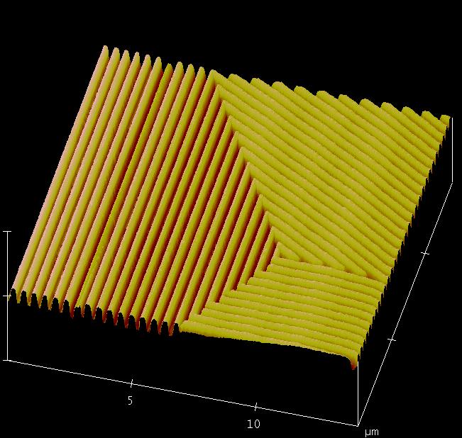
10 RESULTS LINE STRUCTURE Still picture of single-pass cutting on Silicon τ p = 110fs τ p = 500fs τ p = 1ps Chien & Gupta τ p = 5ps τ p = 10ps
11 RESULTS LINE STRUCTURE * Laser cutting on E = 10 µj pass 5-pass 10-pass Pulse width (ps) pass 5-pass 10-pass Pulse width (ps) Chien & Gupta


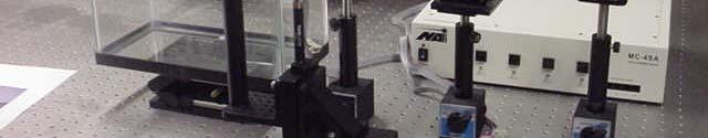
12 LASER PEENING SET UP Bugayev and Gupta
13 X-RAY DIFFRACTION PATTERN of 316L 16 DIFFRACTED BEAM (a.u.) [111] [200] STEEL 316L before LSP after LSP [220] Θ (degree) Bugayev and Gupta
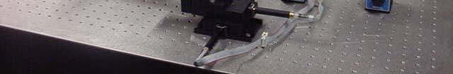
14 Fs Laser Holography Bugayev and Gupta
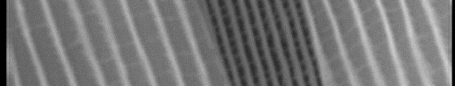
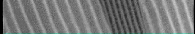
15 Fs Laser Holography 0.48 mm Bugayev and Gupta

16 Balance photodiode Input laser Probe beam Xu and Gupta
17 7 Power Absorption Spectrum 6 Room temperature water vapor Frequency (THz) Xu and Gupta
18 Aim: To improve the efficiency of Si solar cells. Diode Laser Laser Crystallization of a-si:h Set up Method: Crystallize a-si:h using a semiconductor laser. Diode Array Laser Beam Path Focusing Lens a-si:h film Sponsor: National Science Foundation Result CPS [a.u] Advantages: - Manufacturing Compatibility -Solar cell Stability. [111] 2θ XRD of crystallized Si Nayak & Gupta

19 Butterfly Color Formation Wong and Gupta


20 Butterfly Surface under SEM Wong and Gupta

21 Grating Fabrication Wong and Gupta
22 121.6 nm VUV Lamp Chamber for MIT-Lincoln Lab RF Input VUV Radiation for Materials Processing Si Detector Discharge Chamber Gas Input Spectra Pressure = 500 Torr Flowrate = 900 Sccm 0.058% H2 RF = 60 W 10 5 Yan and Gupta Wavelength (nm) Supported by DARPA


23 Some Experiments on Plasma Interaction with Materials RF input power 150W, Ar silicon plate 0.5mm T = 1683 K Akhmerov and Gupta


24 Yang and Gupta Plasma Modification of Surfaces Rotary stage Polymer film Plasma jet Roller


25 Plasma Processing Oxygen Treated Untreated PET Fluorochemical Yang, Mohajer and Gupta Teflon
Bioimaging of cells and tissues using accelerator-based sources
 Analytical and Bioanalytical Chemistry Electronic Supplementary Material Bioimaging of cells and tissues using accelerator-based sources Cyril Petibois, Mariangela Cestelli Guidi Main features of Free
Demonstration of exponential growth and saturation at VUV wavelengths at the TESLA Test Facility Free-Electron Laser. P. Castro for the TTF-FEL team
 Demonstration of exponential growth and saturation at VUV wavelengths at the TESLA Test Facility Free-Electron Laser P. Castro for the TTF-FEL team 100 nm 1 Å FEL radiation TESLA Test Facility at DESY
Outline of the proposed JLAMP VUV/soft X-ray FEL and the challenges for the photon beamlines and optics
 Outline of the proposed JLAMP VUV/soft X-ray FEL and the challenges for the photon beamlines and optics J. Michael Klopf Jefferson Lab - Free Electron Laser Division Workshop on Future Light Sources SLAC
GaN-based Schottky diodes for EUV/VUV/UV photodetection
 1 GaN-based Schottky diodes for EUV/VUV/UV photodetection F. Shadi Shahedipour-Sandvik College of Nanoscale Science and Engineering University at Albany - SUNY, Albany NY 12203 cnse.albany.edu sshahedipour@uamail.albany.edu
SYNTHESIS AND ANALYSIS OF SILICON NANOWIRES GROWN ON Si (111) SUBSTRATE AT DIFFERENT SILANE GAS FLOW RATE
 SUBSTRATE AT DIFFERENT SILANE GAS FLOW RATE") SYNTHESIS AND ANALYSIS OF SILICON NANOWIRES GROWN ON Si (111) SUBSTRATE AT DIFFERENT SILANE GAS FLOW RATE Habib Hamidinezhad*, Yussof Wahab, Zulkafli Othaman and Imam Sumpono Ibnu Sina Institute for Fundamental
SYNTHESIS AND ANALYSIS OF SILICON NANOWIRES GROWN ON Si (111) SUBSTRATE AT DIFFERENT SILANE GAS FLOW RATE Habib Hamidinezhad*, Yussof Wahab, Zulkafli Othaman and Imam Sumpono Ibnu Sina Institute for Fundamental
High Rep-Rate KrF Laser Development and Intense Pulse Interaction Experiments for IFE*
 High Rep-Rate KrF Laser Development and Intense Pulse Interaction Experiments for IFE* Y. Owadano, E. Takahashi, I. Okuda, I. Matsushima, Y. Matsumoto, S. Kato, E. Miura and H.Yashiro 1), K. Kuwahara 2)
Romania and High Power Lasers Towards Extreme Light Infrastructure in Romania
 Romania and High Power Lasers Towards Extreme Light Infrastructure in Romania Razvan Dabu, Daniel Ursescu INFLPR, Magurele, Romania Contents GiWALAS laser facility TEWALAS laser facility CETAL project
Innovations in Laser Technologies and European scale
 Vilnius Innovation Forum, 3-4 September, 2015 Innovations in Laser Technologies and European scale Dr. Gediminas Račiukaitis Head of Department of Laser Technologies Center for Physical Sciences and Technology
Lecture 19 Optical Characterization 1
 Lecture 19 Optical Characterization 1 1/60 Announcements Homework 5/6: Is online now. Due Wednesday May 30th at 10:00am. I will return it the following Wednesday (6 th June). Homework 6/6: Will be online
COMMISSIONING STATUS AND FURTHER DEVELOPMENT OF THE NOVOSIBIRSK MULTITURN ERL*
 COMMISSIONING STATUS AND FURTHER DEVELOPMENT OF THE NOVOSIBIRSK MULTITURN ERL* O.A.Shevchenko #, V.S.Arbuzov, E.N.Dementyev, B.A.Dovzhenko, Ya.V.Getmanov, E.I.Gorniker, B.A.Knyazev, E.I.Kolobanov, A.A.Kondakov,
Atlantic. Industrial High Power Picosecond Lasers. features
 Industrial High Picosecond Lasers lasers have been designed as a versatile tool for a variety of industrial material processing applications. They are compact, OEM rugged, with up to 6 W output power at
Enable Highly-Stable Plasma Operations at High Pressures with the Right RPS Solution
 Enable Highly-Stable Plasma Operations at High Pressures with the Right RPS Solution Created by Advanced Energy Industries, Inc., Fort Collins, CO Abstract Conventional applications for remote plasma sources
Jian-Wei Liu, Jing Zheng, Jin-Long Wang, Jie Xu, Hui-Hui Li, Shu-Hong Yu*
 Supporting Information Ultrathin 18 O 49 Nanowire Assemblies for Electrochromic Devices Jian-ei Liu, Jing Zheng, Jin-Long ang, Jie Xu, Hui-Hui Li, Shu-Hong Yu* Experimental Section Synthesis and Assembly
Microprobe-enabled Terahertz sensing applications
 Microprobe-enabled Terahertz sensing applications World of Photonics, Laser 2015, Munich Protemics GmbH Aachen, Germany Terahertz microprobing technology: Taking advantage of Terahertz range benefits without
Japan Update. EUVA (Extreme Ultraviolet Lithography System Development Association) Koichi Toyoda. SOURCE TWG 2 March, 2005 San Jose
 Koichi Toyoda. SOURCE TWG 2 March, 2005 San Jose") 1 Japan Update EUVA (Extreme Ultraviolet Lithography System Development Association) Koichi Toyoda SOURCE TWG 2 March, 2005 San Jose Outline 2 EUVA LPP at Hiratsuka R&D Center GDPP at Gotenba Branch Lab.
1 Japan Update EUVA (Extreme Ultraviolet Lithography System Development Association) Koichi Toyoda SOURCE TWG 2 March, 2005 San Jose Outline 2 EUVA LPP at Hiratsuka R&D Center GDPP at Gotenba Branch Lab.
A novel High Average Power High Brightness Soft X-ray Source using a Thin Disk Laser System for optimized Laser Produced Plasma Generation
 A novel High Average Power High Brightness Soft X-ray Source using a Thin Disk Laser System for optimized Laser Produced Plasma Generation I. Mantouvalou, K. Witte, R. Jung, J. Tümmler, G. Blobel, H. Legall,
Supplementary Materials for
 advances.sciencemag.org/cgi/content/full/4/2/e1700324/dc1 Supplementary Materials for Photocarrier generation from interlayer charge-transfer transitions in WS2-graphene heterostructures Long Yuan, Ting-Fung
LUCX - THZ PROGRAM: OVERVIEW AND PROSPECTS
 LUCX - THZ PROGRAM: OVERVIEW AND PROSPECTS A. Aryshev On behalf of QB group and THz collaboration 14 Outline THz project overview LUCX activity LUCX Projects Overview THz program LUCX Laser system LUCX
Solar Cells, Modules, Arrays, and Characterization
 ... energizing Ohio for the 21st Century Solar Cells, Modules, Arrays, and Characterization April 17, 2014 The University of Toledo, Department of Physics and Astronomy SSARE, PVIC Principles and Varieties
Monolithically integrated InGaAs nanowires on 3D. structured silicon-on-insulator as a new platform for. full optical links
 Monolithically integrated InGaAs nanowires on 3D structured silicon-on-insulator as a new platform for full optical links Hyunseok Kim 1, Alan C. Farrell 1, Pradeep Senanayake 1, Wook-Jae Lee 1,* & Diana.
NIST EUVL Metrology Programs
 NIST EUVL Metrology Programs S.Grantham, C. Tarrio, R.E. Vest, Y. Barad, S. Kulin, K. Liu and T.B. Lucatorto National Institute of Standards and Technology (NIST) Gaithersburg, MD USA L. Klebanoff and
Femtosecond laser microfabrication in. Prof. Dr. Cleber R. Mendonca
 Femtosecond laser microfabrication in polymers Prof. Dr. Cleber R. Mendonca laser microfabrication focus laser beam on material s surface laser microfabrication laser microfabrication laser microfabrication
PGx11 series. Transform Limited Broadly Tunable Picosecond OPA APPLICATIONS. Available models
 PGx1 PGx3 PGx11 PT2 Transform Limited Broadly Tunable Picosecond OPA optical parametric devices employ advanced design concepts in order to produce broadly tunable picosecond pulses with nearly Fourier-transform
Evaluation of high power laser diodes for space applications: effects of the gaseous environment
 Evaluation of high power laser diodes for space applications: effects of the gaseous environment Jorge Piris, E. M. Murphy, B. Sarti European Space Agency, Optoelectronics section, ESTEC. M. Levi, G. Klumel,
FLASH II. FLASH II: a second undulator line and future test bed for FEL development.
 FLASH II FLASH II: a second undulator line and future test bed for FEL development Bart.Faatz@desy.de Outline Proposal Background Parameters Layout Chalenges Timeline Cost estimate Personnel requirements
Supporting Information. Epitaxially Aligned Cuprous Oxide Nanowires for All-Oxide, Single-Wire Solar Cells
 Supporting Information Epitaxially Aligned Cuprous Oxide Nanowires for All-Oxide, Single-Wire Solar Cells Sarah Brittman, 1,2 Youngdong Yoo, 1 Neil P. Dasgupta, 1,3 Si-in Kim, 4 Bongsoo Kim, 4 and Peidong
Designing for Femtosecond Pulses
 Designing for Femtosecond Pulses White Paper PN 200-1100-00 Revision 1.1 July 2013 Calmar Laser, Inc www.calmarlaser.com Overview Calmar s femtosecond laser sources are passively mode-locked fiber lasers.
Atlantic. Industrial High Power Picosecond Lasers. features
 Atlantic Industrial High Picosecond Lasers lasers have been designed as a versatile tool for a variety of industrial material processing applications. They are compact, OEM rugged, with up to 8 W output
Digital multimirror devices for precision laser micromachining
 Digital multimirror devices for precision laser micromachining Rob Eason, Ben Mills, Matthias Feinäugle, Dan Heath, Collin Sones, James Grant-Jacob, Ioannis Katis, Collin Sones. Optoelectronics Research
On-line spectrometer for FEL radiation at
 On-line spectrometer for FEL radiation at FERMI@ELETTRA Fabio Frassetto 1, Luca Poletto 1, Daniele Cocco 2, Marco Zangrando 3 1 CNR/INFM Laboratory for Ultraviolet and X-Ray Optical Research & Department
The TSIS Spectral Irradiance Monitor: Prism Optical Degradation Studies
 The TSIS Spectral Irradiance Monitor: Prism Optical Degradation Studies Lo Erik Richard, Dave Harber, Joel Rutkowski, Matt Triplett, Kasandra O Malia Laboratory for Atmospheric and Space Physics (LASP)
Robert G. Hunsperger. Integrated Optics. Theory and Technology. Sixth Edition. 4ü Spri rineer g<
 Robert G. Hunsperger Integrated Optics Theory and Technology Sixth Edition 4ü Spri rineer g< 1 Introduction 1 1.1 Advantages of Integrated Optics 2 1.1.1 Comparison of Optical Fibers with Other Interconnectors
Generation of a Line Focus for Material Processing from an Array of High Power Diode Laser Bars R. Baettig, N. Lichtenstein, R. Brunner, J.
 Generation of a Line Focus for Material Processing from an Array of High Power Diode Laser Bars R. Baettig, N. Lichtenstein, R. Brunner, J. Müller, B. Valk, M. Kreijci, S. Weiss Overview This slidepack
SNV/U High Performances UV Microchip Series
 SNV/U High Performances UV Microchip Series Key features 355nm and 266nm Repetition rate up to 20kHz Ultrashort pulses down to 550ps Multi-kW peak power Excellent beam quality Efficient, air-cooled Sealed
Development of a high-power coherent THz sources and THz-TDS system on the basis of a compact electron linac
 Development of a high-power coherent THz sources and THz-TDS system on the basis of a compact electron linac Masafumi Kumaki A) Ryunosuke Kuroda B), Hiroyuki Toyokawa B), Yoshitaka Taira B), Kawakatsu
Supplementary Materials for
 advances.sciencemag.org/cgi/content/full/3/10/eaao4204/dc1 Supplementary Materials for Enhanced mobility CsPbI3 quantum dot arrays for record-efficiency, high-voltage photovoltaic cells Erin M. Sanehira,
Atlantic. series. Industrial High Power Picosecond DPSS Lasers
 Atlantic series Industrial High Power Picosecond DPSS Lasers Laser description Laser micromachining is rapidly becoming the material processing technology of choice for numerous small scale, real world
Silicon Light Machines Patents
 820 Kifer Road, Sunnyvale, CA 94086 Tel. 408-240-4700 Fax 408-456-0708 www.siliconlight.com Silicon Light Machines Patents USPTO No. US 5,808,797 US 5,841,579 US 5,798,743 US 5,661,592 US 5,629,801 US
k λ NA Resolution of optical systems depends on the wavelength visible light λ = 500 nm Extreme ultra-violet and soft x-ray light λ = 1-50 nm
 Resolution of optical systems depends on the wavelength visible light λ = 500 nm Spatial Resolution = k λ NA EUV and SXR microscopy can potentially resolve full-field images with 10-100x smaller features
Development of scalable laser technology for EUVL applications
 Development of scalable laser technology for EUVL applications Tomáš Mocek, Ph.D. Chief Scientist & Project Leader HiLASE Centre CZ.1.05/2.1.00/01.0027 Lasers for real-world applications Laser induced
Atlantic. Industrial High Power Picosecond Lasers. features
 Atlantic Industrial High Power Picosecond Lasers lasers have been designed as a versatile tool for a variety of industrial material processing applications. They are compact, OEM rugged, with up to 8 W
Progress in High Gradient Accelerator Research at MIT
 Progress in High Gradient Accelerator Research at MIT Presented by Richard Temkin MIT Physics and Plasma Science and Fusion Center May 23, 2007 MIT Accelerator Research Collaborators MIT Plasma Science
Dual Vivaldi UWB nanoantenna for optical applications
 Dual Vivaldi UWB nanoantenna for optical applications Zeev Iluz, Yuval Yifat, Doron Bar-Lev, Michal Eitan, Yoni Kantarovsky, Yuav Blue, Yael Hanein, Koby Scheuer, and Amir Boag School of Electrical Engineering
Electromagnetic Applications in Nanotechnology
 Electromagnetic Applications in Nanotechnology Carbon nanotubes (CNTs) Hexagonal networks of carbon atoms 1nm diameter 1 to 100 microns of length Layer of graphite rolled up into a cylinder Manufactured:
Consortium Capabilities
 Consortium Capabilities The driver in advanced materials development is to create products with competitive advantages. Products must continuously become faster, lighter and cheaper and must provide additional
SUPPLEMENTARY INFORMATION
 SUPPLEMENTARY INFORMATION doi:10.1038/nature10864 1. Supplementary Methods The three QW samples on which data are reported in the Letter (15 nm) 19 and supplementary materials (18 and 22 nm) 23 were grown
12/08/2003 H. Schlarb, DESY, Hamburg
 K. Bane, F.-J. Decker, P. Emma, K. Hacker, L. Hendrickson,, C. L. O Connell, P. Krejcik,, H. Schlarb*, H. Smith, F. Stulle*, M. Stanek, SLAC, Stanford, CA 94025, USA * σ z NDR 6 mm 1.2 mm 3-stage compression
Theoretical Approach. Why do we need ultra short technology?? INTRODUCTION:
 Theoretical Approach Why do we need ultra short technology?? INTRODUCTION: Generating ultrashort laser pulses that last a few femtoseconds is a highly active area of research that is finding applications
Waveguide-Integrated Optical Antenna nanoleds for On-Chip Communication
 Waveguide-Integrated Optical Antenna nanoleds for On-Chip Communication Michael Eggleston, Kevin Messer, Seth Fortuna, Eli Yablonovitch, Ming C. Wu Department of Electrical Engineering and Computer Sciences
FLASH at DESY. FLASH. Free-Electron Laser in Hamburg. The first soft X-ray FEL operating two undulator beamlines simultaneously
 FLASH at DESY The first soft X-ray FEL operating two undulator beamlines simultaneously Katja Honkavaara, DESY for the FLASH team FEL Conference 2014, Basel 25-29 August, 2014 First Lasing FLASH2 > First
Arūnas Krotkus Center for Physical Sciences & Technology, Vilnius, Lithuania
 Arūnas Krotkus Center for Physical Sciences & Technology, Vilnius, Lithuania Introduction. THz optoelectronic devices. GaBiAs: technology and main physical characteristics. THz time-domain system based
Nuclear Instruments and Methods in Physics Research A
 Nuclear Instruments and Methods in Physics Research A 729 (2013) 19 24 Contents lists available at ScienceDirect Nuclear Instruments and Methods in Physics Research A journal homepage: www.elsevier.com/locate/nima
CALIBRATION OF TERAHERTZ SPECTROMETERS
 CALIBRATION OF TERAHERTZ SPECTROMETERS Mira Naftaly and Richard A. Dudley National Physical Laboratory, Teddington TW LW, UK Corresponding author: mira.naftaly@npl.co.uk Abstract Calibration methods for
TIME-PRESERVING MONOCHROMATORS FOR ULTRASHORT EXTREME-ULTRAVIOLET PULSES
 TIME-PRESERVING MONOCHROMATORS FOR ULTRASHORT EXTREME-ULTRAVIOLET PULSES Luca Poletto CNR - Institute of Photonics and Nanotechnologies Laboratory for UV and X-Ray Optical Research Padova, Italy e-mail:
Fiber Laser Chirped Pulse Amplifier
 Fiber Laser Chirped Pulse Amplifier White Paper PN 200-0200-00 Revision 1.2 January 2009 Calmar Laser, Inc www.calmarlaser.com Overview Fiber lasers offer advantages in maintaining stable operation over
Project: IEEE P Working Group for Wireless Personal Area Networks N
 July, 2008 Project: IEEE P802.15 Working Group for Wireless Personal Area Networks N (WPANs( WPANs) Submission Title: Millimeter-wave Photonics for High Data Rate Wireless Communication Systems Date Submitted:
Introduction to Optoelectronic Devices
 Introduction to Optoelectronic Devices Dr. Jing Bai Assistant Professor Department of Electrical and Computer Engineering University of Minnesota Duluth October 30th, 2012 1 Outline What is the optoelectronics?
Lithography. 3 rd. lecture: introduction. Prof. Yosi Shacham-Diamand. Fall 2004
 Lithography 3 rd lecture: introduction Prof. Yosi Shacham-Diamand Fall 2004 1 List of content Fundamental principles Characteristics parameters Exposure systems 2 Fundamental principles Aerial Image Exposure
THE ORION PHOTOINJECTOR: STATUS and RESULTS
 THE ORION PHOTOINJECTOR: STATUS and RESULTS Dennis T. Palmer SLAC / ARDB ICFA Sardinia 4 July 2002 1. Introduction 2. Beam Dynamics Simulations 3. Photoinjector 1. RF Gun 2. Solenoidal Magnet 3. Diagnostics
DCS laser for Thomson scattering diagnostic applications
 DCS laser for Thomson scattering diagnostic applications Authors Jason Zweiback 10/6/2015 jzweiback@logostech.net 1 Summary Motivation DCS laser Laser for Thomson scattering diagnostics 2 What is the Dynamic
FemtoFAB. Femtosecond laser micromachining system. tel fax Konstitucijos ave. 23C LT Vilnius, Lithuania
 FemtoFAB Femtosecond laser micromachining system Konstitucijos ave. 23C LT-08105 Vilnius, Lithuania tel. +370 5 272 57 38 fax +370 5 272 37 04 info@wophotonics.com www.wophotonics.com INTRODUCTION FemtoFAB
Development of a fast EUV movie camera for Caltech spheromak jet experiments
 P1.029 Development of a fast EUV movie camera for Caltech spheromak jet experiments K. B. Chai and P. M. Bellan ` California Institute of Technology kbchai@caltech.edu Caltech Spheromak gun 2 Target: study
Testing with Femtosecond Pulses
 Testing with Femtosecond Pulses White Paper PN 200-0200-00 Revision 1.3 January 2009 Calmar Laser, Inc www.calmarlaser.com Overview Calmar s femtosecond laser sources are passively mode-locked fiber lasers.
PHGN/CHEN/MLGN 435/535: Interdisciplinary Silicon Processing Laboratory. Simple Si solar Cell!
 Where were we? Simple Si solar Cell! Two Levels of Masks - photoresist, alignment Etch and oxidation to isolate thermal oxide, deposited oxide, wet etching, dry etching, isolation schemes Doping - diffusion/ion
SNP High Performances IR Microchip Series
 SNP High Performances IR Microchip Series Key features Repetition rate up to 130kHz Ultrashort pulses down to 600ps Multi-kW peak power Excellent beam quality, M²
Optical Interconnection in Silicon LSI
 The Fifth Workshop on Nanoelectronics for Tera-bit Information Processing, 1 st Century COE, Hiroshima University Optical Interconnection in Silicon LSI Shin Yokoyama, Yuichiro Tanushi, and Masato Suzuki
POLYMER MICROSTRUCTURE WITH TILTED MICROPILLAR ARRAY AND METHOD OF FABRICATING THE SAME
 POLYMER MICROSTRUCTURE WITH TILTED MICROPILLAR ARRAY AND METHOD OF FABRICATING THE SAME Field of the Invention The present invention relates to a polymer microstructure. In particular, the present invention
Practical Applications of Laser Technology for Semiconductor Electronics
 Practical Applications of Laser Technology for Semiconductor Electronics MOPA Single Pass Nanosecond Laser Applications for Semiconductor / Solar / MEMS & General Manufacturing Mark Brodsky US Application
Precision Cold Ablation Material Processing using High-Power Picosecond Lasers
 Annual meeting Burgdorf Precision Cold Ablation Material Processing using High-Power Picosecond Lasers Dr. Kurt Weingarten kw@time-bandwidth.com 26 November 2009 Background of Time-Bandwidth Products First
Far infrared generation by CO 2 lasers frequencies subtraction in a ZnGeP 2 crystal.
 Far infrared generation by CO 2 lasers frequencies subtraction in a ZnGeP 2 crystal. Yu.A.Shakir V.V.Apollonov A.M.Prokhorov A.G.Suzdal tsev General Physics Institute of RAS, 38 Vavilov st., Moscow 117333,
THz Pump Beam for LCLS. Henrik Loos. LCLS Hard X-Ray Upgrade Workshop July 29-31, 2009
 Beam for LCLS Henrik Loos Workshop July 29-31, 29 1 1 Henrik Loos Overview Coherent Radiation Sources Timing THz Source Performance 2 2 Henrik Loos LCLS Layout 6 MeV 135 MeV 25 MeV 4.3 GeV 13.6 GeV σ z.83
In the name of God, the most merciful Electromagnetic Radiation Measurement
 In the name of God, the most merciful Electromagnetic Radiation Measurement In these slides, many figures have been taken from the Internet during my search in Google. Due to the lack of space and diversity
Drive Beam Photo-injector Option for the CTF3 Nominal Phase
 CTF3 Review Drive Beam Photo-injector Option for the CTF3 Nominal Phase Motivation CTF3 Drive Beam Requirements CTF3 RF gun design The Laser (I. Ross / RAL) The Photocathode Cost estimate Possible schedule
Supplementary Materials for
 www.sciencemag.org/cgi/content/full/science.1234855/dc1 Supplementary Materials for Taxel-Addressable Matrix of Vertical-Nanowire Piezotronic Transistors for Active/Adaptive Tactile Imaging Wenzhuo Wu,
SNP High Performances IR Microchip Series
 SNP High Performances IR Microchip Series KEY FEATURES Repetition rate up to 130 khz Ultrashort pulses down to 600 ps Multi-kW peak power Excellent beam quality, M²
A BaF2 calorimeter for Mu2e-II
 A BaF2 calorimeter for Mu2e-II I. Sarra, on behalf of LNF group Università degli studi Guglielmo Marconi Laboratori Nazionali di Frascati NEWS General Meeting 218 13 March 218 Proposal (1) q This technological
Typical LED Characteristics
 Typical LED Characteristics Characteristic Unit Value Light output 1 mw > 1 2 Peak wavelength 3 nm 255 nm to 28 nm 4 Viewing angle Degrees 11 5 Full width at half maximum 3 (@1 ma) nm 16 Forward voltage
taccor Optional features Overview Turn-key GHz femtosecond laser
 taccor Turn-key GHz femtosecond laser Self-locking and maintaining Stable and robust True hands off turn-key system Wavelength tunable Integrated pump laser Overview The taccor is a unique turn-key femtosecond
Photoresist erosion studied in an inductively coupled plasma reactor employing CHF 3
 Photoresist erosion studied in an inductively coupled plasma reactor employing CHF 3 M. F. Doemling, N. R. Rueger, and G. S. Oehrlein a) Department of Physics, University at Albany, State University of
THz Imaging by a Wide-band Compact FEL
 FEL-2004, Trieste, Italy THz Imaging by a Wide-band Compact FEL 2 Sep. 2004 Young Uk Jeong, Grigori M. Kazakevitch b, Hyuk Jin Cha, Seong Hee Park, and Byung Cheol Lee Korea Atomic Energy Research Institute
Plasma Efficiency and Losses for pulsed Xe Excimer DBDs at high Power Densities
 Plasma Efficiency and Losses for pulsed Xe Excimer DBDs at high Power Densities Mark Paravia, Michael Meisser, Wolfgang Heering GEC, Saratoga Springs 29,, Germany KIT University of the State of Baden-Württemberg
Robert Magnusson, Ph.D.
 Robert Magnusson, Ph.D. Texas Instruments Distinguished University Chair in Nanoelectronics Director of the Nanophotonics Device Group Co-founder and Chief Technical Officer of Resonant Sensors Incorporated
Single frequency MOPA system with near diffraction limited beam
 Single frequency MOPA system with near diffraction limited beam quality D. Chuchumishev, A. Gaydardzhiev, A. Trifonov, I. Buchvarov Abstract Near diffraction limited pulses of a single-frequency and passively
Directional Growth of Ultra-long CsPbBr 3 Perovskite. Nanowires for High Performance Photodetectors
 Supporting information Directional Growth of Ultra-long CsPbBr 3 Perovskite Nanowires for High Performance Photodetectors Muhammad Shoaib, Xuehong Zhang, Xiaoxia Wang, Hong Zhou, Tao Xu, Xiao Wang, Xuelu
Power. Warranty. 30 <1.5 <3% Near TEM ~4.0 one year. 50 <1.5 <5% Near TEM ~4.0 one year
 DL CW Blue Violet Laser, 405nm 405 nm Operating longitudinal mode Several Applications: DNA Sequencing Spectrum analysis Optical Instrument Flow Cytometry Interference Measurements Laser lighting show
Lasers à fibres ns et ps de forte puissance. Francois SALIN EOLITE systems
 Lasers à fibres ns et ps de forte puissance Francois SALIN EOLITE systems Solid-State Laser Concepts rod temperature [K] 347 -- 352 342 -- 347 337 -- 342 333 -- 337 328 -- 333 324 -- 328 319 -- 324 315
Micro-PackS, Technology Platform. Security Characterization Lab Opening
 September, 30 th 2008 Micro-PackS, Technology Platform Security Characterization Lab Opening Members : Micro-PackS in SCS cluster From Silicium to innovative & commucating device R&D structure, gathering
The Department of Advanced Materials Engineering. Materials and Processes in Polymeric Microelectronics
 The Department of Advanced Materials Engineering Materials and Processes in Polymeric Microelectronics 1 Outline Materials and Processes in Polymeric Microelectronics Polymeric Microelectronics Process
H. Lubatschowski T. Ripken, U. Oberheide, C. Ziltz, G. Gerten. Femtosecond Laser Applications in the Huaman Lens
 H. Lubatschowski T. Ripken, U. Oberheide, C. Ziltz, G. Gerten Femtosecond Laser Applications in the Huaman Lens fs-laser induced elasticity changes to improve presbyopic lens accommodation presbyopia material
Polissage et texturation de surface par fusion laser
 Polissage et texturation de surface par fusion laser Christophe ARNAUD, Anthony ALMIRALL, Charly LOUMENA et Rainer KLING C. Arnaud et al., Journal of Laser Applications, Vol. 29, 022501 (2017) Poste laser
PCS-150 / PCI-200 High Speed Boxcar Modules
 Becker & Hickl GmbH Kolonnenstr. 29 10829 Berlin Tel. 030 / 787 56 32 Fax. 030 / 787 57 34 email: info@becker-hickl.de http://www.becker-hickl.de PCSAPP.DOC PCS-150 / PCI-200 High Speed Boxcar Modules
Laser-Produced Sn-plasma for Highvolume Manufacturing EUV Lithography
 Panel discussion Laser-Produced Sn-plasma for Highvolume Manufacturing EUV Lithography Akira Endo * Extreme Ultraviolet Lithography System Development Association Gigaphoton Inc * 2008 EUVL Workshop 11
High Power and Energy Femtosecond Lasers
 High Power and Energy Femtosecond Lasers PHAROS is a single-unit integrated femtosecond laser system combining millijoule pulse energies and high average powers. PHAROS features a mechanical and optical
Broadband Beamforming of Terahertz Pulses with a Single-Chip 4 2 Array in Silicon
 Forum for Electromagnetic Research Methods and Application Technologies (FERMAT) Broadband Beamforming of Terahertz Pulses with a Single-Chip 4 2 Array in Silicon M. Mahdi Assefzadeh and Aydin Babakhani
Infrared Perfect Absorbers Fabricated by Colloidal Mask Etching of Al-Al 2 O 3 -Al Trilayers
 Supporting Information Infrared Perfect Absorbers Fabricated by Colloidal Mask Etching of Al-Al 2 O 3 -Al Trilayers Thang Duy Dao 1,2,3,*, Kai Chen 1,2, Satoshi Ishii 1,2, Akihiko Ohi 1,2, Toshihide Nabatame
Nanoscale Systems for Opto-Electronics
 Nanoscale Systems for Opto-Electronics 675 PL intensity [arb. units] 700 Wavelength [nm] 650 625 600 5µm 1.80 1.85 1.90 1.95 Energy [ev] 2.00 2.05 1 Nanoscale Systems for Opto-Electronics Lecture 5 Interaction
directly on each side of the crystal to form a rugged, monolithic oscillator that is end pumped by a CW diode laser.
 Product Bulletin MicroChip NanoPulse, NanoGreen, and NanoEyeSafe CDRH Solid-State Lasers The JDS Uniphase MicroChip NanoLaser produces high peak power, high repetition rates, and short pulses from compact,
Operating longitudinal mode Several Polarization ratio > 100:1. Power. Warranty. 30 <1.5 <5% Near TEM ~4.0 one year
 DL CW Blue Violet Laser, 405nm 405 nm Operating longitudinal mode Several Applications: DNA Sequencing Spectrum analysis Optical Instrument Flow Cytometry Interference Measurements Laser lighting show
Data sheet for TDS 10XX system THz Time Domain Spectrometer TDS 10XX
 THz Time Domain Spectrometer TDS 10XX TDS10XX 16/02/2018 www.batop.de Page 1 of 11 Table of contents 0. The TDS10XX family... 3 1. Basic TDS system... 3 1.1 Option SHR - Sample Holder Reflection... 4 1.2
EE 143 Microfabrication Technology Fall 2014
 EE 143 Microfabrication Technology Fall 2014 Prof. Clark T.-C. Nguyen Dept. of Electrical Engineering & Computer Sciences University of California at Berkeley Berkeley, CA 94720 EE 143: Microfabrication