Triple i - The key to your success
|
|
|
- Thomasine Bates
- 6 years ago
- Views:
Transcription
1
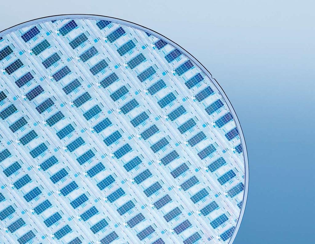
2 Triple i - The key to your success The needs and challenges of today s world are becoming ever more demanding. Standards are constantly rising. Creativity, reliability and high performance are basic prerequisites for a successful future in growth-oriented markets. As a renowned leader in complete process solutions in the fields of microsystems and nanotechnologies, we continually rise to the challenges of the day. Strong partnerships and our power of innovation form the basis for intelligent solutions built with the highest degrees of productivity and quality. Know-how and flexibility lead to cutting-edge innovation in state-of-the-art technologies. Innovative thinking and many years of experience have created an atmosphere in which intelligent solutions are defined and constantly improved. Our philosophy is invent - innovate - implement. 2 3

3 invent There are no limits; only limiting thoughts. Always one step ahead, we push the limits and are at the forefront of setting new standards. We open new paths to the visions of tomorrow. With our equipment and processes, we constantly bring to market emerging applications and develop new technologies in partnership with our customers. 4 5

4 innovate Innovation is dedication and superior competence. Faster than others, we develop new technologies and processes through constant innovation and continuous improvement. Achieving the shortest time lapse between R&D and small-scale production is among our targets. We support our customers in reducing the time it takes to get their products to market. Our creativity and decades of experience enable us not only to meet, but also to outperform the most complex challenges of our customers. 6 7


5 implement Reliability is the demand. Consistently high, trustworthy performance is our response. Our equipment is designed for high volume industrial production. We implement cost efficient large-scale manufacturing technologies for new value-added products to supply our customers industries. As a reliable partner with a high degree of application know-how, we guarantee a high level of security through the optimized system performance of our certified process solutions. We counter the cost factors of uptime and throughput through our proactive approach, while ensuring the highest levels of performance and quality


6 EV Group meets the varied demands of diverse markets. The basis for our success is our products: lithography, bonding and imprint systems. We hold the dominant share of the market for all types of wafer bonding equipment and are the market and technology leader in lithography and nanoimprinting. EVG Markets MEMS (Micro-Electro-Mechanical Systems) MEMS are intelligent, miniaturized 3D devices consisting of microelectronic components (integrated circuits) and micromechanical, optical, chemical, biochemical, or micro-optical compo-nents. MEMS technology is a rapidly emerging field with a high growth rate. Motion sensors, micro mirrors, microphones, gyroscopes, and accelerometers are just a few of the MEMS devices that are found in consumer applications such as cell phones, television sets, digital cameras, gaming devices and laptops. Advanced Packaging, 3D Interconnect Advanced packaging techniques such as wafer bumping, 3D Interconnect, and chip scale packaging allow different components of an integrated circuit (IC) to be stacked on each other and directly connected, rather than side by side on a printed circuit board. These new packaging methods enable the production of ICs with reduced cost, lower power consumption and higher performance. SOI (Silicon On Insulator) SOI technology uses layered siliconinsulator-silicon wafers in place of conventional silicon wafers as a means of producing smaller devices and reducing power consumption. A typical fabrication process for SOI wafers is based on bonding a silicon wafer to an insulating substrate followed by thinning of the topmost Si wafer to the desired thickness. Compound Semiconductor and Silicon-Based Power Devices Compound semiconductors are made from two or more different elements such as gallium arsenide (GaAs). LEDs, laser diodes, and solid-state lasers are examples of devices based on compound semiconductors. Power devices are microelectronic components that are essential functional elements in electrical equipment such voltage converters, power amplifiers, switch-mode power supplies, etc. Essential criteria in power device fabrication are high throughput, yield, process control and quality. Nanotechnology Nanoimprint Lithography (NIL) is one of the most promising and cost-effective new techniques for generating nanometer-scaleresolution patterns for a variety of commercial applications in BioMEMS, microfluidics, micro-optics, and patterned media. Researchers use nanoimprint lithography to produce inexpensive, next-generation nanoelectronic devices. The world of our customers: Automotive Industrial Instrumentation Communication Medical PC/IT Engineered Substrates Home Entertainment Solar

7 Our customers place their confidence in us. Utmost reliability and consistently high performance create an atmosphere of trust. Trust in the concept, development, application, success of the product and trust in the achievement of agreed goals. In close cooperation with our customers, we develop and produce total solutions. We invest 20% of our total annual sales revenue in research and development. This investment allows us to bring our triple-i philosophy (invent-innovate-implement) to life and enables EVG to maintain technological leadership in its markets. Our reliability as a long-term partner and our innovative solutions lead to sustainable long-term growth for our customers. Process know-how is a key factor in achieving shortest time to market. Our comprehensive process knowledge is a result of our decades of experience and creates benefits and advantages for our customers, from development to production. Success is the product of a reliable partnership. Many years of experience provide the key to our success as a total-solution provider from development to turnkey, high-volume solutions to services individually tailored for our customers. Our long-term service strategy includes spare part availability and expert service support. Our customer s confidence and mutual trust guarantee successful products. We know that true success begins with trust.


8 Our highly qualified employees are part of a worldwide network. Commitment without borders. We act globally. Our lithography, bonding and imprint equipment is designed for reliability, productivity and quality, without any limits. Our highly qualified employees are part of a worldwide network and react quickly and flexibly to customer requests and enquiries. We are always prepared for new challenges. Headquarters: EV Group E. Thallner GmbH, DI Erich Thallner Strasse 1, A-4782 St.Florian/Inn, Austria, Phone: , Fax: , Info@EVGroup.com, Web:

9
6-7 October Marina Bay Sands Expo & Convention Centre Peony Ballroom [Level 4]
![6-7 October Marina Bay Sands Expo & Convention Centre Peony Ballroom [Level 4]](/thumbs/80/80853998.jpg "6-7 October Marina Bay Sands Expo & Convention Centre Peony Ballroom [Level 4]") camline http://www.camline.com Booth 22 camline s mission is to provide the highest quality software solutions for factory automation and logistics, helping global manufacturers maintain their competitive
camline http://www.camline.com Booth 22 camline s mission is to provide the highest quality software solutions for factory automation and logistics, helping global manufacturers maintain their competitive
PRESS KIT. High Accuracy Device Bonder with Robotics.
 PRESS KIT High Accuracy Device Bonder with Robotics Press Announcement SET Introduces FC300R High Accuracy Device Bonder with Robotics FC300R: an Easy-to-Use Production Platform Ideal for High Accuracy
Plan Optik AG. Plan Optik AG PRODUCT CATALOGUE
 Plan Optik AG Plan Optik AG PRODUCT CATALOGUE 2 In order to service the high demand of wafers more quickly, Plan Optik provides off the shelf products in sizes from 2 up to 300mm diameter. Therefore Plan
6-7 October Marina Bay Sands Expo & Convention Centre Peony Ballroom [Level 4]
![6-7 October Marina Bay Sands Expo & Convention Centre Peony Ballroom [Level 4]](/thumbs/81/83818377.jpg "6-7 October Marina Bay Sands Expo & Convention Centre Peony Ballroom [Level 4]") camline http://www.camline.com Booth 22 camline s mission is to provide the highest quality software solutions for factory automation and logistics, helping global manufacturers maintain their competitive
camline http://www.camline.com Booth 22 camline s mission is to provide the highest quality software solutions for factory automation and logistics, helping global manufacturers maintain their competitive
POSSUM TM Die Design as a Low Cost 3D Packaging Alternative
 POSSUM TM Die Design as a Low Cost 3D Packaging Alternative The trend toward 3D system integration in a small form factor has accelerated even more with the introduction of smartphones and tablets. Integration
Beam Shaping Excellence
 Beam Shaping Excellence 300 patents 200 employees 13 countries 2 Every photon. In the right place, at the right time. LIMO: The world of beam shaping Whether it's materials processing, illumination or
MEDIA RELEASE FOR IMMEDIATE RELEASE 26 JULY 2016
 MEDIA RELEASE FOR IMMEDIATE RELEASE 26 JULY 2016 A*STAR S IME KICKS OFF CONSORTIA TO DEVELOP ADVANCED PACKAGING SOLUTIONS FOR NEXT-GENERATION INTERNET OF THINGS APPLICATIONS AND HIGH-PERFORMANCE WIRELESS
RealNano & ACINTECH Projektbeispiele für Nanotechnologie in der Mikroelektronik
 RealNano & ACINTECH Projektbeispiele für Nanotechnologie in der Mikroelektronik Reinhold Ebner, Anton Köck, Stefan Defregger Materials Center Leoben Forschung GmbH Roseggerstrasse 12 A-8700 Leoben www.mcl.at
MMIC: Introduction. Evangéline BENEVENT. Università Mediterranea di Reggio Calabria DIMET
 Evangéline BENEVENT Università Mediterranea di Reggio Calabria DIMET 1 Evolution of electronic circuits: high frequency and complexity Moore s law More than Moore System-In-Package System-On-Package Applications
Application-Based Opportunities for Reused Fab Lines
 Application-Based Opportunities for Reused Fab Lines Semicon China, March 17 th 2010 Keith Best Simax Lithography S I M A X A L L I A N C E P A R T N E R S Outline Market: Exciting More than Moore applications
MEMS Sensors: From Automotive. CE Applications. MicroNanoTec Forum Innovations for Industry April 19 th Hannover, Germany
 MEMS Sensors: From Automotive to CE Applications MicroNanoTec Forum Innovations for Industry 2010 April 19 th Hannover, Germany Oliver Schatz, CTO 1 Engineering April 2010 GmbH 2009. All rights reserved,
Contents. Contents. INTRODUCTION Trainer Team Training Facilities. GENERAL COURSES Robot System CAN Bus and CANopen Motion Controllers and Servos
 EV Group Training Courses 2015 Contents Contents INTRODUCTION Trainer Team Training Facilities GENERAL COURSES Robot System CAN Bus and CANopen Motion Controllers and Servos WAFER BONDING SYSTEMS EVG5xx
MEMS in ECE at CMU. Gary K. Fedder
 MEMS in ECE at CMU Gary K. Fedder Department of Electrical and Computer Engineering and The Robotics Institute Carnegie Mellon University Pittsburgh, PA 15213-3890 fedder@ece.cmu.edu http://www.ece.cmu.edu/~mems
HARTING Coaxial and Metric Connectors
 HARTING Coaxial and Metric Connectors HARTING Worldwide Transforming customer wishes into concrete solutions The HARTING Technology Group is skilled in the fields of electrical, electronic and optical
One-Stop-Shop for. Research Fab Microelectronics Germany
 Fraunhofer Group for Microelectronics One-Stop-Shop for Technologies and Systems Research Fab Microelectronics Germany The entire added-value chain for microelectronics and nanoelectronics from a single
THE ARCOR WAY: A PASSION FOR PRECISION
 THE ARCOR WAY: A PASSION FOR PRECISION 1 THE A-TEAM Our entire team is ready to take on your toughest challenges. When you work with our A-Team leaders, you can feel confident that From engineers to project
FRAUNHOFER INSTITUTE FOR PHOTONIC MICROSYSTEMS IPMS. Application Area. Quality of Life
 FRAUNHOFER INSTITUTE FOR PHOTONIC MICROSYSTEMS IPMS Application Area Quality of Life Overlay image of visible spectral range (VIS) and thermal infrared range (LWIR). Quality of Life With extensive experience
FRAUNHOFER GROUP FOR MICROELECTRONICS ONE-STOP-SHOP FOR TECHNOLOGIES AND SYSTEMS
 FRAUNHOFER GROUP FOR MICROELECTRONICS ONE-STOP-SHOP FOR TECHNOLOGIES AND SYSTEMS The entire added-value chain for microelectronics and nanoelectronics from a single provider The Research Fab Microelectronics
TechSearch International, Inc. Corporate Overview E. Jan Vardaman, President
 TechSearch International, Inc. Corporate Overview E. Jan Vardaman, President Corporate Background Founded in 1987 and headquartered in Austin, Texas Recognized around the world as a leading consulting
Midaz Micro-Slab DPSS Lasers:
 Midaz Micro-Slab DPSS Lasers: Higher power & pulse rate for higher speed micromachining Professor Mike Damzen Midaz Laser Ltd 4 June 2008 AILU Meeting Industrial opportunities in laser micro and nano processing
YOUR PARTNER FOR RELIABLE PROCESS SOLUTIONS IN BONDING, SEALING, CASTING AND MORE...
 YOUR PARTNER FOR RELIABLE PROCESS SOLUTIONS IN BONDING, SEALING, CASTING AND MORE... REINHARDT-TECHNIK AND WAGNER WITH EXCELLENT PROSPECTS WHO WE ARE AND WHAT WE STAND FOR Joined materials metals, glass,
Tailor-made R&D Services: Our Areas of Application
 One-Stop-Shop for Technologies and Systems Tailor-made R&D Services: Our Areas of Application Digital Industry: More than Developing Products The traditional industry sector is undergoing a rapid transition
EV Group Solutions for MEMS
 EV Group Solutions for MEMS EV Group Solutions for MEMS Introduction Micro electro mechanical systems (MEMS), sometimes also referred to as micromachines or as micro systems technology (MST), micro optical
Flexible Substrates and SCB-Technology
 Flexible Substrates and SCB-Technology Substrate Technology As requirements are increasing, so are electronic systems becoming smaller and smaller and more complex. In its role as innovative forerunner
Recent Developments in Multifunctional Integration. Stephan Guttowski, Head of Technology Park»Heterointegration«, Fraunhofer FMD
 Recent Developments in Multifunctional Integration Stephan Guttowski, Head of Technology Park»Heterointegration«, Fraunhofer FMD Founding Participants 2 One-Stop-Shop for developments from wafer technologies
More specifically, I would like to talk about Gallium Nitride and related wide bandgap compound semiconductors.
 Good morning everyone, I am Edgar Martinez, Program Manager for the Microsystems Technology Office. Today, it is my pleasure to dedicate the next few minutes talking to you about transformations in future
EV Group. Mask Alignment Systems
 EV Group Mask Alignment Systems EVG Mask Alignment Systems Lithography Introduction EVG s inventions, such as the world s first bottom-side alignment system in 1985, have pioneered and set industry standards
THIS IS INNOVATION Compound Semiconductors
 THIS IS INNOVATION Compound Semiconductors E N A B L I N G This is a quiet industrial revolution, nudging forward the capabilities of the electronics which hide inside nearly every modern day device and
Direct printing tools for flexible hybrid electronics assembly. David Grierson, Ph.D. President & CTO of systemech, LLC
 Direct printing tools for flexible hybrid electronics assembly David Grierson, Ph.D. President & CTO of systemech, LLC We solve the problem of placing ultra-thin, high-performance Si devices onto flexible
 Organic and flexible Electronics in Saxony www.invest-in-saxony.com WElCOME Organic electronics are based on the discovery that specific organic materials possess semiconducting properties. Functional
Final Exam Topics. IC Technology Advancement. Microelectronics Technology in the 21 st Century. Intel s 90 nm CMOS Technology. 14 nm CMOS Transistors
 ANNOUNCEMENTS Final Exam: When: Wednesday 12/10 12:30-3:30PM Where: 10 Evans (last names beginning A-R) 60 Evans (last names beginning S-Z) Comprehensive coverage of course material Closed book; 3 sheets
1.1 PHILOSOPHY OF MICRO/NANOFABRICATION
 CHAPTER Introduction 1 C H A P T E R C O N T E N T S 1.1 Philosophy of Micro/Nanofabrication... 1 1.2 The Industry Science Dualism... 5 1.3 Industrial Applications... 8 1.4 Purpose and Organization of
End-of-line Standard Substrates For the Characterization of organic
 FRAUNHOFER INSTITUTe FoR Photonic Microsystems IPMS End-of-line Standard Substrates For the Characterization of organic semiconductor Materials Over the last few years, organic electronics have become
Otto Bihler Maschinenfabrik GmbH & Co. KG
 Otto Bihler Maschinenfabrik GmbH & Co. KG WELCOME Dear Readers, Welcome to Bihler. For over 60 years, our family-owned company stands for cutting-edge technology made in Germany. More than 1000 employees
Recent Innovations in MEMS Sensors for PNT Applications
 Recent Innovations in MEMS Sensors for PNT Applications Stanford PNT Symposium 2017 Alissa M. Fitzgerald, Ph.D. Founder & CEO amf@amfitzgerald.com Overview Navigation Developments in MEMS gyroscope technology
Chemistry Based on. Toray Profile: Overview and Philosophy
 Toray Profile: Overview and Philosophy Toray Group, headquartered in Tokyo, Japan, is an integrated chemical group. We are involved in global manufacturing, marketing and sales in three business categories
Lithography in our Connected World
 Lithography in our Connected World SEMI Austin Spring Forum TOP PAN P R INTING CO., LTD MATER IAL SOLUTIONS DIVISION Toppan Printing Co., LTD A Broad-Based Global Printing Company Foundation: January 17,
Nanotechnology, the infrastructure, and IBM s research projects
 Nanotechnology, the infrastructure, and IBM s research projects Dr. Paul Seidler Coordinator Nanotechnology Center, IBM Research - Zurich Nanotechnology is the understanding and control of matter at dimensions
MEDIA RELEASE INSTITUTE OF MICROELECTRONICS KICKS OFF COPPER WIRE BONDING CONSORTIUM II TO TACKLE COPPER INTERCONNECTS RELIABILITY ISSUES
 MEDIA RELEASE INSTITUTE OF MICROELECTRONICS KICKS OFF COPPER WIRE BONDING CONSORTIUM II TO TACKLE COPPER INTERCONNECTS RELIABILITY ISSUES 1. Singapore, 25 March, 2013 -- The Institute of Microelectronics
ACCELERATING THE FUTURE OF SEMICONDUCTORS
 ACCELERATING THE FUTURE OF SEMICONDUCTORS 14 PRODUCTION FACILITIES 7R&D FACILITIES 10+ COUNTRIES VERSUM MATERIALS BY THE NUMBERS* *Fiscal year ending September 30, 2018. 250+ CUSTOMERS CORE INDUSTRIES
Low-Cost Far-Infrared FPA based on High-Volume Pressure Sensor Process
 Low-Cost Far-Infrared FPA based on High-Volume Pressure Sensor Process Michael Krueger 1, Ingo Herrmann 1 Robert Bosch GmbH - Automotive Electronics, Tuebinger Str. 13, D-776 Reutlingen, Germany, michael.krueger@de.bosch.com
Press release. New 450 mm positioning system is twice as fast! Revolutionary Twin Gantry from Schneeberger
 Press release New 450 mm positioning system is twice as fast! Revolutionary Twin Gantry from Schneeberger Known for its innovative positioning and motion systems, Swiss firm Schneeberger Linear Technology
Faculty Development Program on Micro-Electro-Mechanical Systems (MEMS Sensor)
") Faculty Development Program on Micro-Electro-Mechanical Systems (MEMS Report MEMS sensors have been dominating the consumer products such as mobile phones, music players and other portable devices. With
Faculty Development Program on Micro-Electro-Mechanical Systems (MEMS Report MEMS sensors have been dominating the consumer products such as mobile phones, music players and other portable devices. With
Infinitely Precise. micrometal. excellence in etching
 Infinitely Precise micrometal excellence in etching A High-Tech Profile Superfine structures and ultra-tight tolerances: precision is our business You give us the specs, and we etch to ultra-tight tolerances.
CORE EXPERTISE IN YOUR TECHNOLOGIES
 CORE EXPERTISE IN YOUR TECHNOLOGIES MERSEN INSIDE MERSEN INSIDE MERSEN INSIDE MERSEN INSIDE CORPORATE PROFILE Global expert in electrical power and advanced materials, Mersen designs innovative solutions
No soft touch only automated systems can boost productivity and quality when lapping/polishing fragile GaAs wafers
 No soft touch only automated systems can boost productivity and quality when lapping/polishing fragile GaAs wafers Author: Mark Kennedy www.logitech.uk.com Overview The processing of GaAs (gallium arsenide)
TAIPRO Engineering. Speaker: M. Saint-Mard Managing director. TAIlored microsystem improving your PROduct
 TAIPRO Engineering MEMS packaging is crucial for system performance and reliability Speaker: M. Saint-Mard Managing director TAIPRO ENGINEERING SA Michel Saint-Mard Administrateur délégué m.saintmard@taipro.be
Technology & Manufacturing
 Technology & Manufacturing Jean-Marc Chery Chief Operating Officer Front-End Manufacturing Unique capability 2 Technology portfolio aligned with application focus areas Flexible IDM model with foundry
Update: SOI Wafer Market Continues Its Growth
 Gartner Dataquest Alert Update: SOI Wafer Market Continues Its Growth The results of Gartner Dataquest's latest survey of the silicon on insulator (SOI) wafer market indicate demand grew 16 percent in
IHP Innovations for High Performance Microelectronics
 IHP Innovations for High Performance Microelectronics IHP - Innovations for High Performance Microelectronics in Frankfurt (Oder) is known for internationally acknowledged research at the highest level.
X-ray Detectors: What are the Needs?
 X-ray Detectors: What are the Needs? Sol M. Gruner Physics Dept. & Cornell High Energy Synchrotron Source (CHESS) Ithaca, NY 14853 smg26@cornell.edu 1 simplified view of the Evolution of Imaging Synchrotron
The SEMATECH Model: Potential Applications to PV
 Continually cited as the model for a successful industry/government consortium Accelerating the next technology revolution The SEMATECH Model: Potential Applications to PV Dr. Michael R. Polcari President
MemsTech MSM3C-S4045 Integrated Silicon Microphone with Supplementary TEM Analysis
 MemsTech MSM3C-S4045 Integrated Silicon Microphone with Supplementary TEM Analysis MEMS Process Review For comments, questions, or more information about this report, or for any additional technical needs
Fraunhofer IZM - ASSID
 FRAUNHOFER-INSTITUT FÜR Zuverlässigkeit und Mikrointegration IZM Fraunhofer IZM - ASSID All Silicon System Integration Dresden Heterogeneous 3D Wafer Level System Integration 3D system integration is one
Guidelines to Promote National Integrated Circuit Industry Development : Unofficial Translation
 Guidelines to Promote National Integrated Circuit Industry Development : Unofficial Translation Ministry of Industry and Information Technology National Development and Reform Commission Ministry of Finance
EE C245 ME C218 Introduction to MEMS Design Fall 2010
 Instructor: Prof. Clark T.-C. Nguyen EE C245 ME C218 Introduction to MEMS Design Fall 2010 Prof. Clark T.-C. Nguyen Dept. of Electrical Engineering & Computer Sciences University of California at Berkeley
Chapter 7 Introduction to 3D Integration Technology using TSV
 Chapter 7 Introduction to 3D Integration Technology using TSV Jin-Fu Li Department of Electrical Engineering National Central University Jungli, Taiwan Outline Why 3D Integration An Exemplary TSV Process
Atotech solutions. Leading plating chemicals, equipment and services. Atotech At a glance
 Atotech solutions Leading plating chemicals, equipment and services Atotech At a glance www.atotech.com Atotech s journey so far 1869 R. Cruickshank Ltd. begins electroplating operations, later rebranded
Atotech solutions. Leading plating chemicals, equipment and services. Atotech At a glance
 Atotech solutions Leading plating chemicals, equipment and services Atotech At a glance www.atotech.com Atotech s journey so far Atotech becomes a stand-alone company 2017 Today #1 in in plating technologies,
INDUSTRIAL IMAGE PROCESSING BUCHANAN
 INDUSTRIAL IMAGE PROCESSING BUCHANAN Industrial Image Processing Image processing is an important efficiency factor in industrial production, whether to support handling processes, the quality control
Model of Open Innovation IMEC IIAP: a View from Russia
 "Again I say to you, that if two of you agree on Earth about anything that they may ask, it shall be done for them by My Father who is in Heaven. Holy Bible, Matthew 18:19 It seems like for the time being
Advanced Packaging Equipment Solder Jetting & Laser Bonding
 Advanced Packaging Equipment Solder Jetting & Laser Bonding www.pactech.comw.pactech.com PacTech Packaging Technologies Pioneering in laser solder jetting technologies since 1995 Our mission is to reshape
ME 434 MEMS Tuning Fork Gyroscope Amanda Bristow Stephen Nary Travis Barton 12/9/10
 ME 434 MEMS Tuning Fork Gyroscope Amanda Bristow Stephen Nary Travis Barton 12/9/10 1 Abstract MEMS based gyroscopes have gained in popularity for use as rotation rate sensors in commercial products like
RF MEMS Simulation High Isolation CPW Shunt Switches
 RF MEMS Simulation High Isolation CPW Shunt Switches Authored by: Desmond Tan James Chow Ansoft Corporation Ansoft 2003 / Global Seminars: Delivering Performance Presentation #4 What s MEMS Micro-Electro-Mechanical
Technology Transfers Opportunities, Process and Risk Mitigation. Radhika Srinivasan, Ph.D. IBM
 Technology Transfers Opportunities, Process and Risk Mitigation Radhika Srinivasan, Ph.D. IBM Abstract Technology Transfer is quintessential to any technology installation or semiconductor fab bring up.
Developing for tomorrow
 Developing for tomorrow Presenting our R&D activities worldwide Introducing technology at Bekaert Research and Development is the key driver of Bekaert s technological leadership. The role of R&D is not
Core Business: Semiconductor-related Inspection Equipment
 Core Business: Semiconductor-related Inspection Equipment Lasertec manufactures unique inspection and measurement systems that incorporate the cutting-edge technologies of applied optics and offers them
420 Intro to VLSI Design
 Dept of Electrical and Computer Engineering 420 Intro to VLSI Design Lecture 0: Course Introduction and Overview Valencia M. Joyner Spring 2005 Getting Started Syllabus About the Instructor Labs, Problem
Industrialization of Micro-Electro-Mechanical Systems. Werner Weber Infineon Technologies
 Industrialization of Micro-Electro-Mechanical Systems Werner Weber Infineon Technologies Semiconductor-based MEMS market MEMS Market 2004 (total 22.7 BUS$) Others mostly Digital Light Projection IR Sensors
EMT 251 Introduction to IC Design
 EMT 251 Introduction to IC Design (Pengantar Rekabentuk Litar Terkamir) Semester II 2011/2012 Introduction to IC design and Transistor Fundamental Some Keywords! Very-large-scale-integration (VLSI) is
LEMNIOV5.TXT. Title: The Next DARPA Revolution: Integrated Microsystems Zachary Lemnios
 Title: The Next DARPA Revolution: Integrated Microsystems Zachary Lemnios The Next DARPA Revolution: Integrated MicroSYSTEMS Zachary J. Lemnios, Director Microsystems Technology Office Defense Advanced
Products for the energy technology of tomorrow. High-voltage bushings for a new energy age
 Products for the energy technology of tomorrow High-voltage bushings for a new energy age 2 About HSP The pillar of your success! The steady growth in population, urbanization and constant increase in
N e w s R e l e a s e
 N e w s R e l e a s e Infineon Austria achieves double-digit growth and takes the vanguard of Industry 4.0 in Austria year-end statement for fiscal year 2014 New Management Board team since April 2014
OMRON's Long - Term Strategy: Value Generation 2020 (VG2020) - 10 years strategy with future trend
 - 10 years strategy with future trend") VABLJENA PREDAVANJA OMRON's Long - Term Strategy: Value Generation 2020 (VG2020) - 10 years strategy with future trend Thorsten Schlüter Area Sales Manager at Omron Electronics GmbH Elisabeth-Selbert-Strasse
VABLJENA PREDAVANJA OMRON's Long - Term Strategy: Value Generation 2020 (VG2020) - 10 years strategy with future trend Thorsten Schlüter Area Sales Manager at Omron Electronics GmbH Elisabeth-Selbert-Strasse
Infineon at a glance
 Infineon at a glance 2017 www.infineon.com We make life easier, safer and greener with technology that achieves more, consumes less and is accessible to everyone. Microelectronics from Infineon is the
TWINSCAN XT:1950i Water-based immersion taken to the max Enabling fast, single-exposure lithography at sub 40 nm
 TWINSCAN XT:1950i Water-based immersion taken to the max Enabling fast, single-exposure lithography at sub 40 nm SEMICON West, San Francisco July 14-18, 2008 Slide 1 The immersion pool becomes an ocean
research in the fields of nanoelectronics
 FRAUNHOFEr center Nanoelectronic Technologies research in the fields of nanoelectronics 1 contents Fraunhofer CNT in Profile 3 Competence Areas Analytics 4 Functional Electronic Materials 5 Device & Integration
Nanostencil Lithography and Nanoelectronic Applications
 Microsystems Laboratory Nanostencil Lithography and Nanoelectronic Applications Oscar Vazquez, Marc van den Boogaart, Dr. Lianne Doeswijk, Prof. Juergen Brugger, LMIS1 Dr. Chan Woo Park, Visiting Professor
... from Design to Implementation
 ... from Design to Implementation WALLRAM Wear-resistant carbide and ceramic products WALLRAM is a member of the WALLRAM Group. The international Group is active in the manufacturing of forming dies (in
Reducing MEMS product development and commercialization time
 Reducing MEMS product development and commercialization time Introduction Fariborz Maseeh, Andrew Swiecki, Nora Finch IntelliSense Corporation 36 Jonspin Road, Wilmington MA 01887 www.intellisense.com
Knives for the Veneer and Plywood Industry
 Knives for the Veneer and Plywood Industry Knives for the veneer and plywood industry 2 3 Precision and Perfection: For optimal cutting performance, surface consistency and longevity. Our in-depth understanding
Hermetic Packaging Solutions using Borosilicate Glass Thin Films. Lithoglas Hermetic Packaging Solutions using Borosilicate Glass Thin Films
 Hermetic Packaging Solutions using Borosilicate Glass Thin Films 1 Company Profile Company founded in 2006 ISO 9001:2008 qualified since 2011 Headquarters and Production in Dresden, Germany Production
SUSS MA/BA Gen4 Series COMPACT MASK ALIGNER PLATFORM FOR RESEARCH AND LOW-VOLUME PRODUCTION
 SEMI-AUTOMATED MASK ALIGNER SUSS MA/BA Gen4 Series COMPACT MASK ALIGNER PLATFORM FOR RESEARCH AND LOW-VOLUME PRODUCTION SEMI-AUTOMATED MASK ALIGNER SUSS MA/BA Gen4 Series SMART FULL-FIELD EXPOSURE TOOL
IMPACT OF 450MM ON CMP
 IMPACT OF 450MM ON CMP MICHAEL CORBETT MANAGING PARTNER LINX CONSULTING, LLC MCORBETT@LINX-CONSULTING.COM PREPARED FOR CMPUG JULY 2011 LINX CONSULTING Outline 1. Overview of Linx Consulting 2. CMP Outlook/Drivers
THE LONG VIEW IN BRIEF
 THE LONG VIEW IN BRIEF April 2016 WORLD LEADER IN GASES, TECHNOLOGIES AND SERVICES FOR INDUSTRY AND HEALTH, AIR LIQUIDE IS PRESENT IN 80 COUNTRIES WITH MORE THAN 50,000 EMPLOYEES AND SERVES MORE THAN 2
IBM Research - Zurich Research Laboratory
 October 28, 2010 IBM Research - Zurich Research Laboratory Walter Riess Science & Technology Department IBM Research - Zurich wri@zurich.ibm.com Outline IBM Research IBM Research Zurich Science & Technology
SiTime SIT8002AC-13-18E50 One Time Programmable Oscillator
 SiTime SIT8002AC-13-18E50 MEMS Process Review For comments, questions, or more information about this report, or for any additional technical needs concerning semiconductor technology, please call Sales
INSPECTION AND REVIEW PORTFOLIO FOR 3D FUTURE
 INSPECTION AND REVIEW PORTFOLIO FOR 3D FUTURE This week announced updates to four systems the 2920 Series, Puma 9850, Surfscan SP5 and edr-7110 intended for defect inspection and review of 16/14nm node
Fabricating 2.5D, 3D, 5.5D Devices
 Fabricating 2.5D, 3D, 5.5D Devices Bob Patti, CTO rpatti@tezzaron.com Tezzar on Semiconduct or 04/15/2013 1 Gen4 Dis-Integrated 3D Memory DRAM layers 42nm node 2 million vertical connections per lay per
MEMS On-wafer Evaluation in Mass Production Testing At the Earliest Stage is the Key to Lowering Costs
 MEMS On-wafer Evaluation in Mass Production Testing At the Earliest Stage is the Key to Lowering Costs Application Note Recently, various devices using MEMS technology such as pressure sensors, accelerometers,
Layout Analysis Floorplan
 Sample Report Analysis from a Touch Screen Controller For any additional technical needs concerning semiconductor and electronics technology, please call Sales at Chipworks. 3685 Richmond Road, Suite 500,
Finishing first how automated systems improve the productivity and repeatability of wafer lapping and polishing
 Finishing first how automated systems improve the productivity and repeatability of wafer lapping and polishing Author: Mark Kennedy www.logitech.uk.com Overview The lapping and polishing of wafers for
WORKING TODAY FOR A BETTER TOMORROW. What we do
 What we do WORKING TODAY FOR A BETTER TOMORROW Eisenmann is a world leader in surface finishing, material flow automation, thermal process technology, and environmental engineering. For around 65 years,
Lecture: Integration of silicon photonics with electronics. Prepared by Jean-Marc FEDELI CEA-LETI
 Lecture: Integration of silicon photonics with electronics Prepared by Jean-Marc FEDELI CEA-LETI Context The goal is to give optical functionalities to electronics integrated circuit (EIC) The objectives
IHP Innovations for High Performance Microelectronics
 IHP Innovations for High Performance Microelectronics The IHP performs research and development in the fields of silicon-based systems, highest-frequency integrated circuits, and technologies for wireless
CITATION OF PRESIDENT S SCIENCE AND TECHNOLOGY MEDAL 2012 WINNER
 CITATION OF PRESIDENT S SCIENCE AND TECHNOLOGY MEDAL 2012 WINNER Professor Dim-Lee Kwong Executive Director, Institute of Microelectronics, Agency for Science, Technology and Research (A*STAR) For his
Developments, Applications and Challenges for the Industrial Implementation of Nanoimprint Lithography
 Developments, Applications and Challenges for the Industrial Implementation of Nanoimprint Lithography Martin Eibelhuber, Business Development Manager m.eibelhuber@evgroup.com Outline Introduction Imprint
The Department of Advanced Materials Engineering. Materials and Processes in Polymeric Microelectronics
 The Department of Advanced Materials Engineering Materials and Processes in Polymeric Microelectronics 1 Outline Materials and Processes in Polymeric Microelectronics Polymeric Microelectronics Process
LED Cost and Technology Trends: How to enable massive adoption in general lighting
 LED Cost and Technology Trends: How to enable massive adoption in general lighting SEMICON West 2011 Moscone Center, San Francisco June 13 th 2011 Lumileds Lumileds OSRAM Aixtron CREE OSRAM OKI OSRAM 45
Emerging Technologies
 Emerging Technologies & Security Dr. Richard Van Atta Introduction to Emerging Technologies Panel PACOM Operational S&T Conference July 16, 2008 Assessing Emerging Tech Understanding emerging technologies