Inkjet resist inks. Krishna Balantrapu
|
|
|
- Mavis Jackson
- 6 years ago
- Views:
Transcription

1 Inkjet resist inks Krishna Balantrapu
2 OUTLINE Conventional Vs. Inkjet-Cost Savings Inkjet Material Design Inkjet Equipment-Lunaris Future work 2


3 DOW-R&D DRIVERS FOR NEW PRODUCT DEVELOPMENT Technology Need Requirements for end device New specifications New material choices Smaller feature size Different feature shape New equipment sets Environmental New legislative requirements Expense in waste treating Concern regarding hazards REACH and RoHS Cost Raw material costs high Fluctuating prices Reduce risk
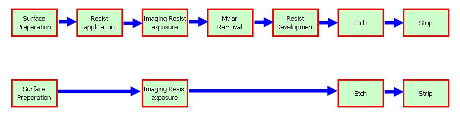
4 CONVENTIONAL Vs. INKJET ETCH RESIST Dry film Process New Inkjet Process 4 - Do not share without permission

5 LEAN MANUFACTURING WITH INKJET 35 Average Minutes Cycle Time/Panel for Imaging Conventional LDI Lunaris *For conventional processing, imaging includes lamination, artwork exposure, mylar peel, developing, and first artcle check. LDI is the same sequence minus first article. Lunaris on the other hand, is just one simple step. 5
6 LABOR COST Throughput Dry Film (manual) Dry Film (automatic) LDI Inkjet Panel output/ hr Production hrs/day Labor Photo plotter Pre-clean & Laminate Printing DES AOI Labor cost/panel $ 4.14 $ 6.21 $ 4.83 $ 1.38 Labor cost/year $828,000 1,242,000 $ 966,000 $ 276,000
7 PROCESS CHEMISTRY COSTS Process step Liters/day of waste Annual cost of chemicals & waste treatment Inkjet material costs Pre-clean 120 $14,300 $7,150 Pre-clean rinse 3600 $4,100 $2,050 Comments No micro etch Vs. dry film Developer 310 $12, Develop rinse 3600 $3, Etcher 1440 $182,400 $182,400 Etching rinse 3600 $4,900 $4,900 Stripper Stripper rinse $17,700 $4,050 $8,850 $2,025 Inkjet strips as sheets Ink thickness is 50% of dry film resist Total $243,050 $207,375 1 m/min line speed@ 35 micron Cu per side and 18 X 24 panels
8 OVERALL SAVINGS OF JET-RESIST ENABLED PCB FAB FACTORY First fully digital, green, automated PCB factory in the world 3-4 year ROI vs China Outsource at Whelen Avg Cost per 18" x 24" Panel $70 $60 $50 $40 $30 $20 $10 $0 China Outsource Whelen Captive Shop

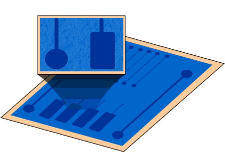
9 CONNECTOR REEL TO REEL PLATING-LITHOJET 250 Band masking seepage Coating in non functional areas


10 CONVENTIONAL MASKING VS. INKJET PLATING RESIST Physical masking Inkjet masking Spot/brush plating tank Gold Inkjet resist Print heads Gold plating tank Resist strip tank Gold Excessive gold bleed ZERO gold bleed Set up time too long Mobile unit which can be fit in any connector line Cannot be used for tight geometries Excessive mask maintenance Excess gold still has to be recovered Coverage zone capability on connector parts ranges from 250 X 250 µm to 3 X 3 Alignment accuracy of ± 100 µm Can be used at line speeds up to 35ft/min No gold recovery step
11 Cost savings/line Line speed (ft/min) Annual ink volume ( kg) Annual Au cost ( 30 µin thick and 20% seepage) kg $ kg $ kg $ kg $ Calculations based on: Strip width: 1 Resist thickness : 15 µm Metal area after connector is formed: 50% Plated area after connector is formed: 20% of metal Masking area : ~ 60% of the metal Working days:
12 12


13 ADVANTAGE FOR HIGH RESOLUTION DESIGN General Inkjet ink LithoJet System Inkjet Head Inkjet Head LithoJet material is formulated for minimizing spreading after jetting After jetting, Ink is spreading. à Limitation for high resolution 13


14 PRE-TREATMENT No shorts or Cu spots due to the lock-in resist to a salt spot since there is no developer No redeposit of debris prior to etch 14
15 MECHANIAL STRENGTH Pencil hardness after UV cure 3 H 15

16 CHEMICAL RESISTANCE S LithoJet ink on High Carbon Steel following an aggressive Ferric Chloride Etch S Etch Depth is approx. 20 mils deep S Good Ink integrity after etching S Customers have had success with etching times over 3 hours Ink Overhang 16
17 POST ETCH RESULTS


18 MATERIAL WASTE COMPARISON ETCH RESIST Inkjet Functional Material Conventional 25 µm Dry Film Inkjet Resist LithoJet inks are 100% solids and do not contain any VOCs 18


19 PACKAGING COMPARISON Dry Film Roll 24 in x 500 ft = 167 panels Includes: Box, End Caps, Core, Wrapper, PET Cover Sheet, and Release Sheet Inkjet container 750g = 300 panels double sided Inkjet ink saves a lot of storage space and storage costs associated with the dry film No cold storage required for LithoJet inks 19
20 LITHOJET 223 ETCH RESIST Inkjet Head Type Jetting Temperature 8-10 cp) Viscosity at Room Temp. Surface Tension Feature Resolution Curing Energy Curing / Pinning Wavelength Pencil Hardness after Curing Color Etch Compatibility Stripping Method Stripping Time Plating Compatibility Applied Thickness Stability At Jetting Temperature Dimatix, OCE, Xerox, Piezoelectric heads C Semi-solid below 60C ~ dynes/cm 30 µm printed gap; 70 µm printed feature (SE-128) mj/cm 365 nm peak UVA and/or UVB H-3H (Cure Dependent) Blue Green Acid copper etch and alkaline ammoniacal etch Surface strip 50 C. Strips as insoluble particles ~60-90 sec. with spray agitation Acid and Alkaline Plating compatible ~ µm (dpi dependant) ~ 10 days 20


21 ADVANTAGES OF LITHOJET Photolithography Alternative Faster Job Turns Direct CAD to image Shorter change-over times Reduced Work In Process (WIP) Smaller batch sizes become practical Green Chemistry 100% solids, no VOCs Low waste, low process steps Achieve High Resolution Advantages of Hot Melt low spread Higher Yields Elimination of repeating mask defects Reduction in alignment / scaling defects Possibility for Various Electronic Devices Fabrication 21
22 22
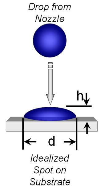
23 PIEZOELECTRIC INKJET DROP EJECTION Drop-on-Demand printing deposits single drops of material Primary technique for electronic imaging is a piezoelectric inkjet print head 1. Rest 2. Fill Chamber 3. Fire 4. Drop Eject Voltage Standard Square Wave Rise Time Pulse Width 23 Fall Time
24 WHAT YOU SEE IS WHAT YOU ETCH Pre etch* Post etch* Resist line width (track) 100 µm 75 µm Line width variation 3σ +/- 10 µm 3σ +/- 10 µm* Space (gap) 50 µm 75 µm Front-to-Back Alignment +/- 15 µm Same-Side Alignment +/- 10 µm Full IQI (AOI) Yes Throughput cores/hour ** 50 Throughput sides/hour ** 100 Substrate size 24 X 24 Panel thickness 0,035 2,5 mm * Typical 2 ounce copper example from Beta Site. Lower cu weights will have better tolerances ** Panel size 610 x 533 mm


25 PATENTED INKJET TECHNOLOGY Without a Print Strategy. CAM data Raster data Nozzle output Etch Resist Uncontrolled flow With Advanced Print Strategy. CAM data Raster data Inkflow calculations based on procédé 26pl drop 65µm spot 10µm panel accuracy Output
26 RESOLUTION IN SCAN DIRECTION Combination of table speed and frequency results in Y-dpi Frequency in Hertz dpi = Table speed in in/sec 30 pl Head Drops merge ~ 500 dpi with 50um drop size Example One: f=1500 Hz dpi = 1500/10 = 225 Table speed = 10 m/min Example Two: f=3000 Hz dpi = 3000/10 = 450 Table speed = 10 m/min Thickness of ink will increase due to overlap! Example Three: f=6000 Hz dpi = 60000/10 = 900 Table speed = 10 m/min 26


27 RESOLUTION IN ORTHOGONAL DIRECTION Example 20 mils = 50 dpi native Spectra SE-128 One head / One pass 10 mils = 100 dpi interlaced 2nd head / 2nd pass 27


28 PRINTED LINES Edge roughness <10 µm pre-etch 2 8


29 REDUNDANCY 20 heads printing 40 heads predicting 3 heads positioned same raster line 60 heads, nozzles in a virtual beam

 Check for Shorts & Filter")
30 100% IMAGE QUALITY INSPECTION Inline-product AOI: IQI Check against CAM Info Check at process speed for errors Detect Opens & Mouse Bites (Missing ink) Text Used for Product Calibration Approval of every printed panel (prior to etching) Check for Shorts & Filter Spots 3 0

31 WHELEN The first fully digital inner and outer layer printer based on ink-jet technology Area requirement placement :6000x3600x3000 mm (LxBxH)

32 LUNARIS IN PRODUCTION 32

33 ROADMAP 33


34 34
The Use of Inkjet Printing Technology for Fabricating Electronic Circuits The Promise and the Practical
 The Use of Inkjet Printing Technology for Fabricating Electronic Circuits The Promise and the Practical Brian Amos Engineering Manager, Dow Electronic Materials, Marlborough, MA, USA Thomas Sutter Emerging
PCB Fabrication Processes Brief Introduction
 PCB Fabrication Processes Brief Introduction AGS-Electronics, Ph: +1-505-550-6501 or +1-505-565-5102, Fx: +1-505-814-5778, Em: sales@ags-electronics.com, Web: http://www.ags-electronics.com Contents PCB
Major Fabrication Steps in MOS Process Flow
 Major Fabrication Steps in MOS Process Flow UV light Mask oxygen Silicon dioxide photoresist exposed photoresist oxide Silicon substrate Oxidation (Field oxide) Photoresist Coating Mask-Wafer Alignment
MICROBUMP CREATION SYSTEM FOR ADVANCED PACKAGING APPLICATIONS
 MICROBUMP CREATION SYSTEM FOR ADVANCED PACKAGING APPLICATIONS Andrew Ahr, EKC Technology, & Chester E. Balut, DuPont Electronic Technologies Alan Huffman, RTI International Abstract Today, the electronics
Ricoh Industrial Ink Jet Technology
 Ricoh Industrial Ink Jet Technology Ink Jet Business Division EMEA IMI Barcelona, November 2014 Presentation Outline HISTORY & ORGANIZATION SOLUTIONS TECHNOLOGY Who is Ricoh? Founded in 1936 108,000+ Employees
Printing as a material deposition process
 Printing as a material deposition process Printing Materials, Mumbai 5 th March 2011 Prof. Fritz Bircher, www.printtechnology.ch 1 Presentation outline Material deposition The inkjet printing process Interaction
Inkjet Printing of Ag Nanoparticles using Dimatix Inkjet Printer, No 1
 University of Pennsylvania ScholarlyCommons Protocols and Reports Browse by Type 1-13-2017 using Dimatix Inkjet Printer, No 1 Amal Abbas amalabb@seas.upenn.edu Inayat Bajwa inabajwa@seas.upenn.edu Follow
Part 5-1: Lithography
 Part 5-1: Lithography Yao-Joe Yang 1 Pattern Transfer (Patterning) Types of lithography systems: Optical X-ray electron beam writer (non-traditional, no masks) Two-dimensional pattern transfer: limited
VELOX IDS 250. Direct-to-shape digital decoration for mass production of cylindrical containers. Unprecedented decoration quality
 VELOX IDS 250 Direct-to-shape digital decoration for mass production of cylindrical containers Unprecedented decoration quality Total operational agility Low total cost of ownership DIGITAL PACKAGING DECORATION
Photolithography Technology and Application
 Photolithography Technology and Application Jeff Tsai Director, Graduate Institute of Electro-Optical Engineering Tatung University Art or Science? Lind width = 100 to 5 micron meter!! Resolution = ~ 3
CLAIMS 1. A suspension board with circuit, characterized in that, it comprises a metal support layer, an insulating layer formed on the metal support
 [19] State Intellectual Property Office of the P.R.C [51] Int. Cl 7 G11B 5/48 H05K 1/11 [12] Patent Application Publication G11B 21/16 [21] Application No.: 00133926.5 [43] Publication Date: 5.30.2001
HIGH QUALITY LABEL PRINTING WITH OUTSTANDING PRECISION.
 LABEL PRINTERS HIGH QUALITY LABEL PRINTING WITH OUTSTANDING PRECISION. Explore a world of having an exceptional print quality across a wide range of label substrates with consistent colour reproduction
Inkjet Filling of TSVs with Silver Nanoparticle Ink. Behnam Khorramdel, Matti Mäntysalo Tampere University of Technology ESTC 2014 Finland, Helsinki
 Inkjet Filling of TSVs with Silver Nanoparticle Ink Behnam Khorramdel, Matti Mäntysalo Tampere University of Technology ESTC 2014 Finland, Helsinki Outline Motivation for this study Inkjet in MEMS fabrication
Printing versus coating technology Which way Printed Electronics with solution coating will go?
 Printing versus coating technology Which way Printed Electronics with solution coating will go? Frank Schäfer, Andrea Glawe, Dr. Daniel Eggerath, KROENERT GmbH& Co KG, Schuetzenstrasse 105, 22761 Hamburg
DIGITAL PACKAGING DECORATION
 DIGITAL PACKAGING DECORATION Direct-to-shape digital decoration for mass production of cylindrical containers Unprecedented decoration quality Total operational agility Low total cost of ownership DIGITAL
Visual Imaging in the Electronic Age
 Visual Imaging in the Electronic Age ART 2107, ARCH 3702, CS 1620, ENGRI 1620 3D Printing November 6, 2014 Prof. Donald P. Greenberg dpg5@cornell.edu Types of 3D Printers Selective deposition printers
FAQs. General. Highcon Products
 General 1. Who is Highcon? Highcon is an Israeli company, founded in 2009, that invented the first digital cutting and creasing machines for folding carton finishing and commercial applications the Highcon
Visual Imaging in the Electronic Age
 Visual Imaging in the Electronic Age ART 2107, ARCH 3702, CS 1620, ENGRI 1620 3D Printing October 20, 2015 Prof. Donald P. Greenberg dpg5@cornell.edu Types of 3D Printers Selective deposition printers
Contrast Enhancement Materials CEM 365HR
 INTRODUCTION In 1989 Shin-Etsu Chemical acquired MicroSi, Inc. including their Contrast Enhancement Material (CEM) technology business*. A concentrated effort in the technology advancement of a CEM led
HEAD TECHNOLOGY ALL IN ONE, USER & ENVIRONMENTAL FRIENDLY DESIGN
 SupraQ Series, 2600S & 3300S Supra Imagination Speed is just a part of it!! With an innovative printing technology and outstanding features, SupraQ is created as an excellent choice in the market. The
ESCC2006 European Supply Chain Convention
 ESCC2006 European Supply Chain Convention PCB Paper 20 Laser Technology for cutting FPC s and PCB s Mark Hüske, Innovation Manager, LPKF Laser & Electronics AG, Germany Laser Technology for cutting FPCs
Fully Printed Conformal Antenna and Sensors on 3D Plastic, Ceramic, and Metallic Substrates. Mike O Reilly
 Fully Printed Conformal Antenna and Sensors on 3D Plastic, Ceramic, and Metallic Substrates Mike O Reilly imaps NE 2016 Antenna and sensor printing via Aerosol Jet Optomec has developed high volume 3D
Direct Printing Technology
 Direct Printing Technology A new dimension for aircraft decoration VILF Jahrestagung 2018 Matthias OTTO Multi-Programme Paint Center Hamburg 08. November 2018 External Paint General paint process Roll
The Impact of Reduced Solder Alloy Powder Size on Solder Paste Print Performance. Presented by Karl Seelig, V.P. Technology AIM Metals & Alloys
 The Impact of Reduced Solder Alloy Powder Size on Solder Paste Print Performance Presented by Karl Seelig, V.P. Technology AIM Metals & Alloys Solder Powder Solder Powder Manufacturing and Classification
Advances in Laser Micro-machining for Wafer Probing and Trimming
 Advances in Laser Micro-machining for Wafer Probing and Trimming M.R.H. Knowles, A.I.Bell, G. Rutterford & A. Webb Oxford Lasers June 10, 2002 Oxford Lasers June 2002 1 Introduction to Laser Micro-machining
How an ink jet printer works
 How an ink jet printer works Eric Hanson Hewlett Packard Laboratories Ink jet printers are the most common type of printing devices used in home environments, and they are also frequently used personal
Jet Press 720S. Production features
 Jet Press 720S Production features Jet Press 720S is built for high quality, short run print High quality print Turn jobs around quickly Integrate with existing production Application flexibility Environment
Safety. Set-up time R&D. Quality. Operator Friendly. Flexibility. Web Handling. Reliability. IMAGE TO PRINT 19 th September 2018
 Safety Set-up time Quality Flexibility IMAGE TO PRINT 19 th September 2018 R&D Operator Friendly Web Handling Reliability We want to make our packaging safe!! How do we reach safety? For sure the quality
Section 2: Lithography. Jaeger Chapter 2. EE143 Ali Javey Slide 5-1
 Section 2: Lithography Jaeger Chapter 2 EE143 Ali Javey Slide 5-1 The lithographic process EE143 Ali Javey Slide 5-2 Photolithographic Process (a) (b) (c) (d) (e) (f) (g) Substrate covered with silicon
Passive Direct Print Sensors
 Passive Wireless Sensor Technology Workshop June 6-7, 2012 Hyatt Regency, La Jolla, CA Passive Direct Print Sensors Mike Newton mnewton@nscrypt.com nscrypt Inc. Orlando, Florida University of Texas at
PHOTO ETCHING BRASS Jerry Gilland Boulder Model Railroad Club Aug. 22, 2013
 PHOTO ETCHING BRASS Jerry Gilland Boulder Model Railroad Club Aug. 22, 2013 Big Boy Running Gear All Brass Etched Nickel Plated Note Surface Relief Riverboat Connecting Rod Brass Etched Joseph Henry Riverboat
with even higher quality.
 Digital Inkjet Label Press Makes short-run label printing more efficient and profitable, with even higher quality. Featuring an Epson Micro Piezo Multi-Print Head Array that is built for extreme durability,
Applications of Maskless Lithography for the Production of Large Area Substrates Using the SF-100 ELITE. Jay Sasserath, PhD
 Applications of Maskless Lithography for the Production of Large Area Substrates Using the SF-100 ELITE Executive Summary Jay Sasserath, PhD Intelligent Micro Patterning LLC St. Petersburg, Florida Processing
PAGE 1/6 ISSUE Jul SERIES Micro-SPDT PART NUMBER R516 XXX 10X R 516 _ 1 0 _
 PAGE 1/6 ISSUE Jul-24-2017 SERIES Micro-SPDT PART NUMBER R516 XXX 10X R516 series: the RAMSES concept merges with the SLIM LINE technology, breaking up the frequency limits of SMT switches : - FULL SMT
The Swiss Army Knife for the Lab Micro Material Processing with the LPKF ProtoLaser U4
 The Swiss Army Knife for the Lab Micro Material Processing with the LPKF ProtoLaser U4 Micro Machining in the Lab LPKF ProtoLasers have been in use in leading electronics laboratories around the world
Infinitely Precise. micrometal. excellence in etching
 Infinitely Precise micrometal excellence in etching A High-Tech Profile Superfine structures and ultra-tight tolerances: precision is our business You give us the specs, and we etch to ultra-tight tolerances.
MGI JETVARNISH 3DS. The Ultimate Inkjet Spot Varnish Solution
 The Ultimate Inkjet Spot Varnish Solution MGI JETVARNISH 3DS With print prices steadily declining, printers need new ways to boost revenue and increase profit margins. The MGI JETVARNISH 3DS gets it done
Processes for Flexible Electronic Systems
 Processes for Flexible Electronic Systems Michael Feil Fraunhofer Institut feil@izm-m.fraunhofer.de Outline Introduction Single sheet versus reel-to-reel (R2R) Substrate materials R2R printing processes
PHGN/CHEN/MLGN 435/535: Interdisciplinary Silicon Processing Laboratory. Simple Si solar Cell!
 Where were we? Simple Si solar Cell! Two Levels of Masks - photoresist, alignment Etch and oxidation to isolate thermal oxide, deposited oxide, wet etching, dry etching, isolation schemes Doping - diffusion/ion
Technology Behind the Digital Magic
 Technology Behind the Digital Magic A Crash Course on Industrial Printing John Sweeterman General Manager Digital Division INX International Ink Co Deliver a Unique Experience for Everyone Why make the
Michael R. Creeden CEO/CID+ San Diego PCB, Inc. & EPTAC (858)
") Michael R. Creeden CEO/CID+ San Diego PCB, Inc. & EPTAC mike.creeden@sdpcb.com (858)271-5722 1. Why we collaborate? 2. When do we collaborate? 3. Who do we collaborate with? 4. What do we collaborate?
Michael R. Creeden CEO/CID+ San Diego PCB, Inc. & EPTAC mike.creeden@sdpcb.com (858)271-5722 1. Why we collaborate? 2. When do we collaborate? 3. Who do we collaborate with? 4. What do we collaborate?
HOTBAR REFLOW SOLDERING
 HOTBAR REFLOW SOLDERING Content 1. Hotbar Reflow Soldering Introduction 2. Application Types 3. Process Descriptions > Flex to PCB > Wire to PCB 4. Design Guidelines 5. Equipment 6. Troubleshooting Guide
Innovative pcb solutions used in medical and other devices Made in Switzerland
 Innovative pcb solutions used in medical and other devices Made in Switzerland Chocolate Watches Money.PCB`s innovative pcb`s... Customer = innovation driver Need to add more parts and I/O make smaller/thinner
Semiconductor Manufacturing Technology. Semiconductor Manufacturing Technology. Photolithography: Resist Development and Advanced Lithography
 Semiconductor Manufacturing Technology Michael Quirk & Julian Serda October 2001 by Prentice Hall Chapter 15 Photolithography: Resist Development and Advanced Lithography Eight Basic Steps of Photolithography
Bumping of Silicon Wafers using Enclosed Printhead
 Bumping of Silicon Wafers using Enclosed Printhead By James H. Adriance Universal Instruments Corp. SMT Laboratory By Mark A. Whitmore DEK Screen Printers Advanced Technologies Introduction The technology
Making a Material Difference
 Making a Material Difference Founded as a QinetiQ corporate investment in January 2002 Spun out in 2007 Locations: Rochester, NYS, USA (HQ and Production) Farnborough and Malvern, UK (R&D, Production and
PCB Production Methods
 PCB Production Methods PCB Development Process Summary Manufacturing Constraints Gerber Schematic Board Manufacture This is art! Ensure that the schematic is accurate. Run the ERC often. This is art! Ensure
Lecture 7. Lithography and Pattern Transfer. Reading: Chapter 7
 Lecture 7 Lithography and Pattern Transfer Reading: Chapter 7 Used for Pattern transfer into oxides, metals, semiconductors. 3 types of Photoresists (PR): Lithography and Photoresists 1.) Positive: PR
DIGITAL SPOT UV COATING, EMBOSSING AND HOT FOIL STAMPING
 DIGITAL SPOT UV COATING, EMBOSSING AND HOT FOIL STAMPING THE MGI JETVARNISH 3DS AND IFOIL S. MORE THAN A GAME CHANGER. IT S A GROWTH ENGINE FOR YOUR BUSINESS. Inline spot UV coater. Hot foil stamping.
Section 2: Lithography. Jaeger Chapter 2 Litho Reader. The lithographic process
 Section 2: Lithography Jaeger Chapter 2 Litho Reader The lithographic process Photolithographic Process (a) (b) (c) (d) (e) (f) (g) Substrate covered with silicon dioxide barrier layer Positive photoresist
PRINTED ELECTRONICS 3
 PRINTED ELECTRONICS 3 4 INKTEC PRINTED ELECTRONICS 5 6 INKTEC PRINTED ELECTRONICS 7 InkTec Leads New Paradigm in Printed Electronic Materials Applications OTFT, Memory Cell, Display, RFID and so on Product
Printing Processes and their Potential for RFID Printing
 Printing Processes and their Potential for RFID Printing Anne Blayo and Bernard Pineaux, EFPG 1 - Printing processes - A.Blayo and B. Pineaux - soc -EUSAI - 12th October 2005, Grenoble Outline General
ADVANCED DIRECT IMAGING HIGH POWER UV LEDS. by ALTIX. ntone 186 C ntone cool gray 9C de produit : 40833
 HIGH POWER UV LEDS ntone 186 C ntone cool gray 9C de produit : 40833 ADVANCED DIRECT IMAGING by ALTIX Enhanced 4 LEDs Photo Heads for Higher Productivity and Printing Quality ADVANCED DIRECT IMAGING by
Azura TU. Designed for high-volume printing, simplified platemaking and uncompromising quality, Azura TU outperforms every other plate in its class.
 Designed for high-volume printing, simplified platemaking and uncompromising quality, outperforms every other plate in its class. www.agfagraphics.com Designed for high-volume printing, simplified platemaking
Section 2: Lithography. Jaeger Chapter 2 Litho Reader. EE143 Ali Javey Slide 5-1
 Section 2: Lithography Jaeger Chapter 2 Litho Reader EE143 Ali Javey Slide 5-1 The lithographic process EE143 Ali Javey Slide 5-2 Photolithographic Process (a) (b) (c) (d) (e) (f) (g) Substrate covered
Preliminary Ideas: PTFE-Based Microwave Laminates and Making Prototypes
 Appendix I Preliminary Ideas: PTFE-Based Microwave Laminates and Making Prototypes A1.1 PTFE Laminates PTFE is a popular abbreviation representing a very useful high frequency material, whose chemical
Printed and Hybrid Integration
 Printed and Hybrid Integration Neil Chilton PhD Technical Director, Printed Electronics Limited, UK Neil.Chilton@PrintedElectronics.com Printed Electronics Limited (PEL) General Overview PEL was founded
TAILORED LABEL CONVERSION
 Océ LabelStream 4000 series TAILORED LABEL CONVERSION BASED ON INKJET DNA NEW Océ LabelStream 4000 series TAILORED LABEL CONVERSION BASED ON INKJET DNA Adapt to CHANGING MARKET DYNAMICS Digital printing
Organic Optical Waveguide Fabrication in a Manufacturing Environment
 Organic Optical Waveguide Fabrication in a Manufacturing Environment Benson Chan, How Lin, Chase Carver, Jianzhuang Huang, Jessie Berry Endicott Interconnect Technologies 1093 Clark Street, Endicott NY
Product Specification - LPS Connector Series
 LPS Product Specification - LPS OVERVIEW The LPS products are solderable versions of those in the Neoconix LPM product series. Also developed for mobile devices and other space-constrained applications,
Key success factors for developing and commercializing a successful aqueous inkjet product: A specialist point of view vs. a generalist perspective
 Key success factors for developing and commercializing a successful aqueous inkjet product: A specialist point of view vs. a generalist perspective Oct 24 th 2018 Hamid M. Shirazi Ph.D. Product Manager,
Digital 2D/3D Spot UV Coater with Inline Hot Foiling
 & Digital 2D/3D Spot UV Coater with Inline Hot Foiling New Expandable Inkjet System Format Up to 75x120 cm/29x47 Innovation in Motion A Technological Revolution... The Technological Revolution: Artificial
Chapter 3 Fabrication
 Chapter 3 Fabrication The total structure of MO pick-up contains four parts: 1. A sub-micro aperture underneath the SIL The sub-micro aperture is used to limit the final spot size from 300nm to 600nm for
XFlex X6 Specifications
 XFlex X6 Specifications 340 430 Max Speed 200 m/min 200 m/min Unwinding roll diameter 1000 mm (40 ) 1000 mm (40 ) Web width 340 mm (13 3/8) 430 mm (17 ) Print width 330 mm (13 ) 420 mm (16,5 ) Infeed /
Technology for the MEMS processing and testing environment. SUSS MicroTec AG Dr. Hans-Georg Kapitza
 Technology for the MEMS processing and testing environment SUSS MicroTec AG Dr. Hans-Georg Kapitza 1 SUSS MicroTec Industrial Group Founded 1949 as Karl Süss KG GmbH&Co. in Garching/ Munich San Jose Waterbury
Holistic View of Lithography for Double Patterning. Skip Miller ASML
 Holistic View of Lithography for Double Patterning Skip Miller ASML Outline Lithography Requirements ASML Holistic Lithography Solutions Conclusions Slide 2 Shrink Continues Lithography keeps adding value
The N610i digital label press
 The N610i digital label press High print quality at flexo speeds ombines the productivity associated with flexo with the flexibility offered by rapid job change digital technology Scan the code to find
Contrast Enhancement Materials CEM 365iS
 INTRODUCTION In 1989 Shin-Etsu Chemical acquired MicroSi, Inc. and the Contrast Enhancement Material (CEM) technology business from General Electric including a series of patents and technologies*. A concentrated
FYS4260/FYS9260: Microsystems and Electronics Packaging and Interconnect. Production of Printed Circuit Boards
 FYS4260/FYS9260: Microsystems and Electronics Packaging and Interconnect Production of Printed Circuit Boards Learning objectives Recap Printed Wiring Board manufacturing process Assembly processes Background
Effect of Corona Treatment on Spreading Behavior of UV Ink over Inkjet Printed Silver Nano-Particle Layer
 Effect of Corona Treatment on Spreading Behavior of UV Ink over Inkjet Printed Silver Nano-Particle Layer Khushbeen Department of Printing Technology GJUS&T, Hisar, Haryana, India Email- khushveen12@gmail.com
Design Analysis Process
 Prototype Design Analysis Process Rapid Prototyping What is rapid prototyping? A process that generates physical objects directly from geometric data without traditional tools Rapid Prototyping What is
ADVANCED MASK MAKING AT RIT. David P. Kanen 5th Year Microelectronic Engineer Student Rochester Institute of Technology ABSTRACT
 ADVANCED MASK MAKING AT RIT David P. Kanen 5th Year Microelectronic Engineer Student Rochester Institute of Technology ABSTRACT This project involved the definition of the steps necessary to generate a
Gallus DCS 340 Digital converting solution
 Gallus DCS 340 Digital converting solution February 2016 Ver. 2016.02.05_3.0 Status quo Conventional presses and job requirements Voice of the Customer Biggest concerns or issues with conventional presses
SurePress L-4033 Digital Label Press VERSATILE PRINTING. CONSISTENT QUALITY.
 SurePress L-4033 Digital Label Press VERSATILE PRINTING. CONSISTENT QUALITY. GO DIGITAL AND BOOST YOUR BOTTOM LINE The SurePress L-4033 Inkjet Digital Label Press makes high-quality short-run printing
AWP TM - DEF/DEW Premium Flexo Plate With Pinning Technology For Clean Transfer
 ASAHI AWP TM - DEF/DEW Premium Flexo Plate With Pinning Technology For Clean Transfer Asahi s AWP TM - DEF/DEW digital flexo plates are part of the premium»pinning Technology for Clean Transfer«plates
Digital Inkjet Spot UV Coater With Tactile Effects and Hot Foil Stamping.
 ENG Digital varnish & ifoil Digital Inkjet Spot UV Coater With Tactile Effects and Hot Foil Stamping. 52x105 cm - 20x42 innovation in motion Take your Prints to.. The Technological Revolution: Artificial
Application Note AN-1011
 AN-1011 Board Mounting Application Note for 0.800mm Pitch Devices For part numbers IRF6100, IRF6100PBF, IR130CSP, IR130CSPPBF, IR140CSP, IR140CSPPBF, IR1H40CSP, IR1H40CSPPBF By Hazel Schofield and Philip
PAGE 1/6 ISSUE SERIES Micro-SPDT PART NUMBER R516 XXX 10X. (All dimensions are in mm [inches]) R 516 _ 1 0 _
![PAGE 1/6 ISSUE SERIES Micro-SPDT PART NUMBER R516 XXX 10X. (All dimensions are in mm [inches]) R 516 _ 1 0 _](/thumbs/96/127769340.jpg "PAGE 1/6 ISSUE SERIES Micro-SPDT PART NUMBER R516 XXX 10X. (All dimensions are in mm [inches]) R 516 _ 1 0 _") PAGE 1/6 ISSUE 15-10-18 SERIES Micro-SPDT PART NUMBER R516 XXX 10X R516 series: the RAMSES concept merges with the SLIM LINE technology, breaking up the frequency limits of SMT switches : - FULL SMT TECHNOLOGY
PAGE 1/6 ISSUE 15-10-18 SERIES Micro-SPDT PART NUMBER R516 XXX 10X R516 series: the RAMSES concept merges with the SLIM LINE technology, breaking up the frequency limits of SMT switches : - FULL SMT TECHNOLOGY
Product Specification - LPM Connector Family
 LPM Product Specification - LPM OVERVIEW Developed for mobile devices and other space-constrained applications, the Neoconix LPM line of connectors feature exceptional X-Y-Z density with a simple, highly
WIFAG-Polytype Technologies AG. WIFAG-Polytype Technologies AG Key Competences in Coating and Digital Printing
 WIFAG-Polytype Technologies AG WIFAG-Polytype Technologies AG Key Competences in Coating and Digital Printing Evolution of WIFAG-Polytype Technologies AG 1904 Founding Company Printing Presses Foundation
Solder Paste Deposits and the Precision of Aperture Sizes
 Solder Paste Deposits and the Precision of Aperture Sizes Ahne Oosterhof Eastwood Consulting Hillsboro, OR, USA ahne@oosterhof.com Stephan Schmidt LPKF Laser & Electronics Tualatin, OR, USA sschmidt@lpkfusa.com
Supporting Information for. Thin, Lightweight, Foldable Thermochromic Displays on Paper
 Supporting Information for Thin, Lightweight, Foldable Thermochromic Displays on Paper Adam C. Siegel, Scott T. Phillips, Benjamin Wiley, and George M. Whitesides Department of Chemistry and Chemical Biology,
Topic 3: Output Devices
 Topic 3: Output Devices 3.1 Introduction Output devices are used to translate computer signals into human readable forms. These devices enable the computer to communicate with the user: - Output: Information
Mimaki JFX Product Presentation
 Mimaki JFX200-2513 Product Presentation A new member joins the JFX family - the JFX200-2513 Mimaki JFX200-2513 JFX200-2513 The low entry model of the JFX line, having the high quality print technology
Simple & Perfect Wide format UV-curable flatbed inkjet printer
 Simple & Perfect Wide format UV-curable flatbed inkjet printer Coming SOON KX7 / KX7-R Large Flatbed with RtoR option New JETRIX KX7 series, Coming with Reliable quality & productivity & functionality
Experiences of users in Digital Radiography
 Computed Radiography Products & Applications Experiences of users in Digital Radiography Jimmy Opdekamp May Jimmy 2006Opdekamp Global Product Manager CR Int l Workshop Imaging NDT Chennai, 25-28 April
COLARIS-NF.MULTI DIGITAL PRINTING & DYEING SYSTEM FOR NARROW FABRICS. ... high speed. ... high quality. ... high efficiency
 COLARIS-NF.MULTI DIGITAL PRINTING & DYEING SYSTEM FOR NARROW FABRICS... high speed... high quality... high efficiency www.zimmer-austria.com 10 May 2016 page 1 COLARIS-NF THE DIGITAL PRINTING SYSTEMS FOR
Introduction of IMS Technology for Advanced Solder Bumping on Wafers / Laminates
 Introduction of IMS Technology for Advanced Solder Bumping on Wafers / Laminates Science & Technology IBM Research Tokyo Yasumitsu Orii, PhD Senju Metal Industry Co.,TW Deputy General Manager Lewis Huang
A novel QA approach to combined In- Line Defect/Pinhole detection and coating Opacity measurement.
 A novel QA approach to combined In- Line Defect/Pinhole detection and coating Opacity measurement. Authors: Mr. Matthieu Richard, Mr. Olivier Porret BOBST, CORES, COntrol & REgister Solutions, Lausanne
SurePress L-4533 Digital Label Press. Versatile printing. Consistent quality.
 SurePress L-4533 Digital Label Press Versatile printing. Consistent quality. Expand your offering and boost your bottom line The SurePress L-4533 inkjet digital label press makes high quality short-run
Until Now There Was No Industrial Digital Printing Solution
 Until Now There Was No Industrial Digital Printing Solution Geert Van den hole Barco Graphics Gent, Belgium The Industrial Printing Market Looking at the digital print world, we clearly distinguish 2 different
THE FINISHING TOUCH MID WEB FINISHING SOLUTION FOR DIGITALLY PRINTED FLEXIBLE PACKAGING AND LABELS.
 THE FINISHING TOUCH MID WEB FINISHING SOLUTION FOR DIGITALLY PRINTED FLEXIBLE PACKAGING AND LABELS. 762MM 30 WIDTH FLEXIBLE PACKAGING LABELS CONFIGURABLE HP INDIGO 20000 COMPATIBLE THE DIGICON 3000 FINISHES
Johnny Shell Vice President, Technical Services SGIA. Option A: Buy a state of the art printing press with every option available.
 High End Screen Printing Johnny Shell Vice President, Technical Services SGIA SGIA.org/Garment 1of 88 Which Will Produce a Better Print? Option A: Buy a state of the art printing press with every option
General Design Rules for Conformal Coating
 General Design Rules for Conformal Coating By Dr Lee Hitchens, Nexus Why it all can go wrong in the design stage for conformal coating Most companies have successfully adopted Design for Manufacture (DFM)
AEROSOL JET PRINTING SYSTEM FOR HIGH SPEED, NON-CONTACT FRONT SIDE METALLIZATION OF SILICON SOLAR CELLS
 AEROSOL JET PRINTING SYSTEM FOR HIGH SPEED, NON-CONTACT FRONT SIDE METALLIZATION OF SILICON SOLAR CELLS Bruce H. King and Stephen M. Barnes Optomec, Inc. 3911 Singer NE, Albuquerque, NM 87109, US Phone
Additional information Indium-free, highly transparent, flexible Cu2O/Cu/Cu2O mesh electrodes for flexible touch screen panels
 Additional information Indium-free, highly transparent, flexible Cu2O/Cu/Cu2O mesh electrodes for flexible touch screen panels By Don-Ju Kim 1, Hyo-Joong Kim 1, Ki-Won Seo 1, Ki-Hyun Kim 2, Tae-Wong Kim
Lecture (03.02) PCB fabrication using. and toner thermal transferee By: Dr. Ahmed ElShafee
 PCB fabrication using. and toner thermal transferee By: Dr. Ahmed ElShafee") Lecture (03.02) PCB fabrication using photo resistive PCB and toner thermal transferee By: Dr. Ahmed ElShafee ١ Dr. Ahmed ElShafee, ACU : Spring 2017, Practical App EE IV photo resistive PCB ٢ Step 1 :
Lecture (03.02) PCB fabrication using photo resistive PCB and toner thermal transferee By: Dr. Ahmed ElShafee ١ Dr. Ahmed ElShafee, ACU : Spring 2017, Practical App EE IV photo resistive PCB ٢ Step 1 :
FUJIFILM Dimatix Technology Integration:
 News Release Editorial Contact: Edward Chrusciel FUJIFILM Dimatix 603-443-5364 echrusciel@dimatix.com FOR IMMEDIATE RELEASE FUJIFILM Dimatix Technology Integration: Helping companies incorporate the power
WOOD 474 Structural Panels. Plywood
 WOOD 474 Structural Panels Plywood 1 Oriented Strand Board Structural panels Plywood Produced from veneers glued together at right angles to maximise stability and strength. Oriented Strand Board (OSB)
EE 143 Microfabrication Technology Fall 2014
 EE 143 Microfabrication Technology Fall 2014 Prof. Clark T.-C. Nguyen Dept. of Electrical Engineering & Computer Sciences University of California at Berkeley Berkeley, CA 94720 EE 143: Microfabrication