Technology Overview. Blind Micro-vias. Embedded Resistors. Chip-on-flex. Multi-Tier Boards. RF Product. Multi-chip Modules. Embedded Capacitance
|
|
|
- Ashley Thomas
- 6 years ago
- Views:
Transcription


1 Blind Micro-vias Embedded Resistors Multi-Tier Boards Chip-on-flex RF Product Multi-chip Modules Embedded Capacitance Technology Overview Fine-line Technology
2 Agenda Corporate Overview Company Profile Standard Technologies Challenging Technologies Extreme Technologies Samples Questions

3 Corporate Overview 30 + Years Experience in Design, Development and Manufacture of Highly-sophisticated Electronic Systems Telecommunications, Medical, Industrial, Transportation and Government Markets Internal Control over Manufacturing Employees
4 Corporate Overview Compunetix, Inc. Chorus Call, Inc. Instrumentation Systems Division Chorus Call, Inc. USA Communication Systems Division Printed Circuit Board Group Video Systems Division Federal Systems Division Chorus Call International Switzerland Germany Italy India South Africa Greece Brazil Canada Australia
5 Company Profile Manufacturing Sales / Marketing Quality Services Engineering Production Global Products Engineering Services Engineering Group Consisting Of 8 Engineers Dedicated To Managing / Fabricating Critical Or Technologically Challenging Projects Company Differentiators PCB Layout & Design To Handle Customer Design Overflow And To Give Support To Customer s Design Group
6 Company Profile SBA/FAR 19 Small Business 38 Years Experience Producing Complex Interconnect Systems Customers in Commercial, Education, Telecommunication, and Government Markets Independent Internal R&D 2006 Revenues: $11.0 Million 80+ Employees 25+ Engineers and Professionals ISO9001:2000 Registered and MIL Spec Certified
7 Quality Certifications Company Profile ISO 9001:2000 Registered UL Certified for Single / Double Sided and Multilayer Boards MIL-P Certified for FR4, Polyimide General Dynamics Land Systems Certified for Prototypes and Production Hamilton Sundstrand Space Certification JPL / NASA Flight Certified General Dynamics UK Award For Best Overall Business Performance 2004 / 2005
8 Types of Business Company Profile Prototypes, Quick Turn & Small To Medium Production Military Spec PCBs Rigid, Flex & Rigid/Flex (Class 2, 3 & Mil Spec) High Layer Count Up to 30 Layers, High Density PCBs Independent Design/Drafting Group Buried Passives High Density Interconnects Multi Chip Modules, Chip-On-Board Engineering / Design Assistance
9 Customer Base Company Profile General Dynamics Land Systems United Kingdom AIS ATP Lockheed Martin DoD / DoE IBM Harris Intel Tektronix Orbital DRS Northrop Grumman Terumo Raytheon L3 Communications Philips Medical Maxtek David Sarnoff Bombardier Teledyne
10 Standard Technologies Technology Can Be Purchased In Volumes Overseas Most US Board Shops Can Produce
11 Standard Technologies Board Material: High Tg FR4 Layer Counts 2 to 12 Layers Trace / Space /.005 on 1 oz. Copper Trace / Space /.004 on 1/2 oz. Copper (inner) BGA s 1.0 mm IPC Class 2 Build Specification Aspect Ratios of < 6:1
12 Challenging Technologies Technology Can Be Purchased In Volumes Overseas From Select Few Sources Few High End US Board Shops Can Produce
13 Challenging Technologies Board Material: Polyimide, Flex, High Speed FR4, Ceramic Filled Materials, Teflon Layer Counts Up To 26 Layers Trace / Space /.004 on 1 oz. Copper Trace / Space /.003 on 1/2 oz. Copper (inner) Trace / Space /.004 on 1/2 oz. Copper (outer) BGA s 0.8 mm IPC Class 3 Build Specification or Mil-Spec Aspect Ratios of < 10:1
14 Challenging Technologies Embedded Passives (Resistors) A True Thin-Film, Nickel-Phosphorous (NiP) Alloy. About 0.1 To 0.4 Microns Of The Alloy Is Electro-Deposited On To The Rough, Or Tooth Side Of Copper Foil During Manufacturing Typical Tolerance Of 10 20% Resistors Tested At Final Test And During Inner Layer OHMEGA-PLY LAMINATE copper resistive material ( micron thick) dielectric substrate copper (EXAMPLE OF AVAILABLE CORE)
15 Challenging Technologies Embedded Passives (Resistors) CURRENT IN COPPER NICKEL RESISTOR DIELECTRIC SUBSTRATE NICKEL RESISTOR DIELECTRIC SUBSTRATE CURRENT OUT COPPER NICKEL RESISTOR DIELECTRIC SUBSTRATE ELECTRIC CURRENT FLOWS THROUGH THE LEAST RESISTIVE MATERIAL COPPER NICKEL COPPER
16 Challenging Technologies Embedded Passives (Resistors) Increased Active Circuit Density Replaces Discrete Resistors Incorporated Within The Board Can Be Placed Under Components Ability To Reduce Board Size Weight Savings Double Sided SMT May Be Converted To Single Sided SMT Improved Electrical Performance Significantly Reduced Signal Path To Resistors Termination Of All Signals Become Possible Low Inductance (Less Than 0.7 nh TYPICAL) Reduced Surface EMI
17 Improved Reliability Challenging Technologies Embedded Passives (Resistors) Elimination Of Solder Joints Excellent Long Term (Trillions Of Component Hours Of Operation) Reliability In Millions Of Circuit Boards In Computer, Consumer, Military And Telecommunications Applications Cost Savings Elimination Of Discrete Resistors Rework Reduction Board Density and/or Size Reduction


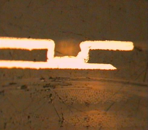
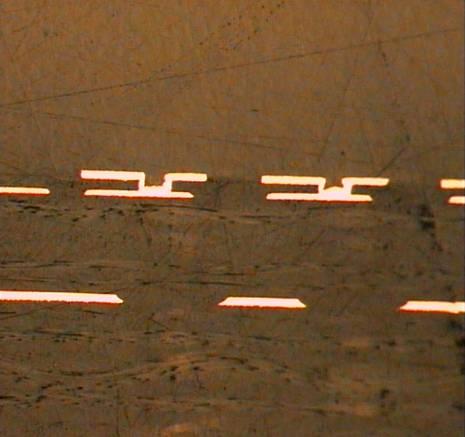
18 Challenging Technologies Embedded Passives (Resistors) Applications Series Termination


19 Challenging Technologies Embedded Passives (Resistors) Applications Parallel Termination
20 Challenging Technologies Embedded Passives (Capacitors) Bulk Capacitance Formed By Placing Power And Ground Layers Close Together Thin Dielectrics Separate Power And Ground To Create Parallel Plate Capacitor C = kea/t Where: C = Capacitance e = Dielectric Constant of Material A = Board Area in Square Inches k = Permittivity of Free Space Constant of 225 t = Dielectric Thickness in inches Cu Film Core Cu Copper clad laminate Double sided (power and ground) Dielectric is a Polyimide and BaTiO composite. Thickness of dielectric is key thinner is better
21 Challenging Technologies Embedded Passives (Capacitors) Reduction In SMT Caps Needed On PCB Closely Spaced Planes Have Lower Inherent Inductance Therefore Supply Current On A Very Short Time Scale Thus Damping Fluctuations Of Voltage At Device Input Low Inductance Planes Reduces EMI Initial Data Indicates That Surface Mounted Capacitance Can Be Effectively Replaced By Embedded Capacitance With Only A Small Fraction Of The Total Discrete Capacitance
22 Products Challenging Technologies Embedded Passives (Capacitors) Properties Product Dupont Interra HK 04 Dupont Interra HK 10 Dupont Interra HK 11 3M C-Ply Capacitance/Area nf/in2 Dielectric Constant Thickness microns Breakdown Voltage Volts Material Dissipation Factor UL Listed Sequential Lam Process >100 Polyimide Poyimide w/filler Poyimide w/filler Ceramic filled Epoxy Yes Yes Pending Yes No Yes Yes Yes


23 Embedded Passives (Capacitors) Application Challenging Technologies Before Embedded Capacitance 18 Layers Blind vias: 1-2, Buried vias 2-17 Over 2000 Caps After Embedded Capacitance 18 Layers No Blind Vias Buried vias 2-17 Removed 800+ Caps
 Controlled Impedance Flex 8 Layers Trace / Space 3.5 / 3.")
24 Challenging Technologies Controlled Impedance Flex Faster Signals with Faster Rise/Fall Times Require Controlled Impedance Flex Cables In Order To Have Cable Flexible, Need To Etch Traces Near 3 mils (Larger Traces Require Thicker Dielectrics For Same Impedance, Making Board Less Flexible) Controlled Impedance Flex 8 Layers Trace / Space 3.5 / 3.5 DuPont AP & LF Flex Material Differential Controlled Impedance

25 Challenging Technologies Rigid-Flex Common Application To Add Reliability And/Or To Reduce Assembly Costs Through Removal Of Connectors And Cabling More Common Due To Tight Spaces And Need For Increased Reliability In Products, Especially In Military Military Avionics Rigid Flex 8 Layers 2 oz. Copper Loose-leaf Design for Increase Flexibility 3 Double Sided Flex Cores w/coverlay Military Specification


26 Challenging Technologies Rigid-Flex Satellite Systems 12 Layers Flight Certified Product Polyimide / DuPont AP Flex Immersion Gold Military 22 Layers 6 Layer Loose-leaf Flex Polyimide / DuPont AP Flex HAL Finish

27 Challenging Technologies High Speed Mixed Material Boards Need For Low Df/Dk Materials for Today s Technology Mix Low Df/Dk, High Cost Material with Higher Df/Dk Low Cost Material Keep Critical Signals on/with Low Df/Dk Material Some Materials can not be Mixed with Certain Other Materials Mixed Material 10Gb Ethernet 8 Layers Blind Vias 1-4 For Stub Control Conductive Epoxy Filled Vias Rogers 4003 / FR4 Material Cavity Construction at Gold Fingers
 Rogers 4000 (Ceramic Filled)")
28 Challenging Technologies High Speed Mixed Material Boards FR4 Material (Glass Bundles) Rogers 4000 (Ceramic Filled)
29 Challenging Technologies Heat Dissipation Boards Smaller Spaces and Hotter Running Parts Require Design Consideration for Heat Dissipation Need To Provide Thermal Path Away From Components Several Design Changes Can be Made To Minimize Thermal Impact to Components Place Heat Generating Part Near Heat Sink or Board Edge Provide Thermal Path In Copper Including Using Edge Plating Use Thermal Vias to Connect to Internal Planes or Heat Sink Use of CB100 for Thermal Vias Heat Sinks Thinner Board Materials Place Component Closer To Heat Sink


30 Challenging Technologies Heat Dissipation Boards Heat Dissipation Board 4 Layers Thin Core FR4 Conductive Epoxy Heat Spreader Attached w/ Thermagon HASL Finish
31 RF Boards Challenging Technologies Boards Typically Made on Teflon or Teflon Blend Products Etching Tolerance of +/ Several Areas of Tight Tolerance Routing +/-.002 (Requires Laser Routing w/vision System Some Designs Require Metal Backing Most Require Wirebondable Gold

32 Challenging Technologies RF Boards Commercial RF 2 Layers Rogers 3003 Laser Routed Slots Trace Tolerance +/ Wirebondable Gold Military RF 4 Layers Rogers 6002, 4350, 4403 Blind 1-2, 4-3; Buried 2-3 Cavity 4 to 3 Trace Tolerance +/ Wirebondable Gold
33 Challenging Technologies Laser Drilled Blind Micro-vias Typically.004 to.006 Laser Drilled Hole From Layers 1 to 2 and/or From N to (N-1) Dielectric Distance.003 to.004 Aspect Ratios less than.50:1 Material Typically RCC (Resin Coated Copper) or Flat Glass FR4 Enables Pin Escaping Small Pitch BGAs or BGAs on Thick PCBs Used to Conserve Routing Channels on Inner Layers Enables Double Sided Assembly in Some Cases
34 Challenging Technologies Laser Drilled Blind Micro-vias
35 Extreme Technologies Overseas Supply Limited to Japan Very Few US Board Shops Can Produce Some Technology Still Under Development

36 Extreme Technologies Chip On Flex (Direct Die Attach) Chip On Flex 2 Layers Trace / Space 2 / 2 2 mil Laser Drilled Vias Wirebondable Gold 2 mil Adhesiveless Pyralux

37 Buried Resistors on Flex Extreme Technologies Buried Resistor on Flex 2 Layers Ohmega Ply Resistor Resistor Covered By Kapton Immersion Silver Finish 2 mil Adhesiveless Pyralux

38 Extreme Technologies Laser Trimmed Embedded Resistors Laser Trimmed Resistors Resistor Laser Trimmed Under Measurement Resistor Trimmed to +/- 1% Final Resistor Tolerance +/- 3% Application: High Speed Testing
39 Copper Filled Micro-vias Extreme Technologies Via-in-pad Provides Flat Pad Surface for BGA Attach Flat Surface Optimal For Stacked Micro-vias Need For Special Plating Chemistry Need For Special Plating Equipment Enables Pin Escaping High Pin Count.5 mm Pitch BGAs Technology Under Development at Several US Shops

40 Copper Filled Micro-vias Current Plating Technology Extreme Technologies

41 Copper Filled Micro-vias Compunetics Test Results Extreme Technologies Test Boards Have Been Received From (2) Chemistry Manufacturers The Smaller The Hole, The More Flat the Plating Plating of Close to 1:1 on Blind Microvias Both Manufacturers to Receive Stacked Microvia Tests Stress Testing In Progress

42 Copper Filled Micro-vias Stacked Micro-vias Extreme Technologies

43 Copper Filled Micro-vias Stepped Micro-vias Extreme Technologies
44 Extreme Technologies High Aspect Ratio Blind Micro-via Plating Some Designs Require More Dielectric Between Layers 1-2 and Still Require Blind Micro-vias Current Technology at approx. 0.7:1 Aspect Ratio Industry Looking for Aspect Ratios of Greater Than 1.25:1 Copper Filled Micro-via Chemistry and Equipment May Help Increase Achievable Aspect Ratios
45 DuPont PF Material All Polyimide Adhesive Extreme Technologies Flex prepreg Without Acrylic Lower Z-axis Expansion Without Acrylic Increase Reliability Much Lower Df (.02 vs..004) Product Withstands MIL-Spec Thermal Shock Testing Product Still In Beta-Test at Several Shops Including Evaluations On-going at Several Large OEMs


46 DuPont PF Material Extreme Technologies Multi-Layer Flex w/ PF Material Multi-Layer Flex w/ LF Bondply
47 Extreme Technologies Fine Line Technology (2 mil Trace/Space & Down) Required for High Pin Count Fine Pitch BGA Routing (<= 0.5 mm Pitch) Chip On Board / Chip On Flex Used To Reduce Layer Count More Tracks per Channel Seen with Laser Drilled Micro-vias Typically on Boards with Small Annular Rings Can be Combined with Embedded Passives

48 Extreme Technologies Laser Ablation Of Soldermask Problem Tighter Pitch Parts Require Better Soldermask Registration Conventional Mask Annular Rings Leave Insufficient Mask Dams Solution BGA Area Covered With Soldermask YAG Laser Used To Remove Mask From BGA Pads Mask Annular Ring Less Than 1 mil Mask Dams Remain Aiding Assembly

49 Extreme Technologies Fine Line Technology (2 mil Trace/Space & Down) Multi-Level Chip Package 6 Layer FR4 2 / 2 Trace / Space Embedded Resistors for Termination Multi-Level Cavity Construction Wirebondable Gold Fine Line Package 1.5 / 1.5 (35 / 35 um) Trace / Space Wirebondable Gold 4 Layers FR4 31 mil Thick +/- 1 mil
50 Ink Jet Printing Extreme Technologies Technology Under Development Printing of: Legend and Soldermask (Near Production) Printing of: Conductors, Resistors, Inductors, etc. (In Development) Advantage: Finer Placement of Material Yields Tighter Tolerance and Finer Features Several Board Shops Helping Industry Develop Technology Inkjet Technology Also Under Development at Several Universities RFID Technology Blind Via Fill

51 Ink Jet Printing Extreme Technologies New System Inkjet Legend Printer Optically Aligned to Panel for Better Registration No Need for Photo-tools or Screens Direct Print From Gerber Files Goal: Thinner / Smaller Characters (Under Development)
PCB technologies and manufacturing General Presentation
 PCB technologies and manufacturing General Presentation 1 Date : December 2014 3 plants for a global offer dedicated to the European market and export Special technologies, Harsh environment PCB for space
CAPABILITIES Specifications Vary By Manufacturing Locations
 Revised June 2011 Toll Free: 1-800-979-4PCB (4722) www.4pcb.com sales@4pcb.com Material FR4 RoHS RF Materials CAPABILITIES Specifications Vary By Manufacturing Locations Number of Conductive Layers Standard
ATTRIBUTES STANDARD ADVANCED
 TECHNOLOGY MATRIX 2017 ATTRIBUTES STANDARD ADVANCED Line/Space.005 /.005.003 /.003 Copper Foil. Oz. Min/Max ½ / 2 3 / 8 Pad Size Int. (dia over Drill).014.008 Pad Size Ext. (dia over Drill).012.008 Drill-to-Metal
Sectional Design Standard for Flexible/Rigid-Flexible Printed Boards
 Sectional Design Standard for Flexible/Rigid-Flexible Printed Boards Developed by the Flexible Circuits Design Subcommittee (D-) of the Flexible Circuits Committee (D-0) of IPC Supersedes: IPC-2223C -
Michael R. Creeden CEO/CID+ San Diego PCB, Inc. & EPTAC (858)
") Michael R. Creeden CEO/CID+ San Diego PCB, Inc. & EPTAC mike.creeden@sdpcb.com (858)271-5722 1. Why we collaborate? 2. When do we collaborate? 3. Who do we collaborate with? 4. What do we collaborate?
Michael R. Creeden CEO/CID+ San Diego PCB, Inc. & EPTAC mike.creeden@sdpcb.com (858)271-5722 1. Why we collaborate? 2. When do we collaborate? 3. Who do we collaborate with? 4. What do we collaborate?
Application Bulletin 240
 Application Bulletin 240 Design Consideration CUSTOM CAPABILITIES Standard PC board fabrication flexibility allows for various component orientations, mounting features, and interconnect schemes. The starting
Generic Multilayer Specifications for Rigid PCB s
 Generic Multilayer Specifications for Rigid PCB s 1.1 GENERAL 1.1.1 This specification has been developed for the fabrication of rigid SMT and Mixed Technology Multilayer Printed Circuit Boards (PCB's)
AltiumLive 2017: Creating Documentation for Successful PCB Manufacturing
 AltiumLive 2017: Creating Documentation for Successful PCB Manufacturing Julie Ellis TTM Field Applications Engineer Thomas Schneider Field Applications Engineer 1 Agenda 1 Complexity & Cost 2 3 4 5 6
Low-Cost PCB Design 1
 Low-Cost PCB Design 1 PCB design parameters Defining PCB design parameters begins with understanding: End product features, uses, environment, and lifetime goals PCB performance, manufacturing, and yield
Overcoming the Challenges of HDI Design
 ALTIUMLIVE 2018: Overcoming the Challenges of HDI Design Susy Webb Design Science Sr PCB Designer San Diego Oct, 2018 1 Challenges HDI Challenges Building the uvia structures The cost of HDI (types) boards
FPGA World Conference Stockholm 08 September John Steinar Johnsen -Josse- Senior Technical Advisor
 FPGA World Conference Stockholm 08 September 2015 John Steinar Johnsen -Josse- Senior Technical Advisor Agenda FPGA World Conference Stockholm 08 September 2015 - IPC 4101C Materials - Routing out from
Innovative pcb solutions used in medical and other devices Made in Switzerland
 Innovative pcb solutions used in medical and other devices Made in Switzerland Chocolate Watches Money.PCB`s innovative pcb`s... Customer = innovation driver Need to add more parts and I/O make smaller/thinner
!"#$"%&' ()#*+,-+.&/0(
#*+,-+.&/0(") !"#$"%&' ()#*+,-+.&/0( Multi Chip Modules (MCM) or Multi chip packaging Industry s first MCM from IBM. Generally MCMs are horizontal or two-dimensional modules. Defined as a single unit containing two
!"#$"%&' ()#*+,-+.&/0( Multi Chip Modules (MCM) or Multi chip packaging Industry s first MCM from IBM. Generally MCMs are horizontal or two-dimensional modules. Defined as a single unit containing two
DESIGN FOR MANUFACTURABILITY (DFM)
") T H A N K S F O R A T T E N D I N G OUR TECHNICAL WEBINAR SERIES DESIGN FOR MANUFACTURABILITY (DFM) Presented by: We don t just sell PCBs. We sell sleep. Cirtech EDA is the exclusive SA representative
T H A N K S F O R A T T E N D I N G OUR TECHNICAL WEBINAR SERIES DESIGN FOR MANUFACTURABILITY (DFM) Presented by: We don t just sell PCBs. We sell sleep. Cirtech EDA is the exclusive SA representative
TCLAD: TOOLS FOR AN OPTIMAL DESIGN
 TCLAD: TOOLS FOR AN OPTIMAL DESIGN THINGS TO CONSIDER WHEN DESIGNING CIRCUITS Many factors come into play in circuit design with respect to etching, surface finishing and mechanical fabrication processes;
BGA (Ball Grid Array)
") BGA (Ball Grid Array) National Semiconductor Application Note 1126 November 2002 Table of Contents Introduction... 2 Package Overview... 3 PBGA (PLASTIC BGA) CONSTRUCTION... 3 TE-PBGA (THERMALLY ENHANCED
BGA (Ball Grid Array) National Semiconductor Application Note 1126 November 2002 Table of Contents Introduction... 2 Package Overview... 3 PBGA (PLASTIC BGA) CONSTRUCTION... 3 TE-PBGA (THERMALLY ENHANCED
Novel Substrate with Combined Embedded Capacitance and Resistance for Better Electrical Performance and Higher Integration
 Novel Substrate with Combined Embedded Capacitance and Resistance for Better Electrical Performance and Higher Integration John Andresakis, Pranabes Pramanik Oak-Mitsui Technologies, LLC Dan Brandler,
Artwork: (A/W) An accurately scaled configuration used to produce the artwork master or production master.
 An accurately scaled configuration used to produce the artwork master or production master.") Adhesive: The material used for bonding two substrates of material together. (usually; LF of FR 0100) Adhesive Squeeze-Out: Adhesive will ooze out slightly during the lamination cycle. Annular Ring: That
Adhesive: The material used for bonding two substrates of material together. (usually; LF of FR 0100) Adhesive Squeeze-Out: Adhesive will ooze out slightly during the lamination cycle. Annular Ring: That
CIRCUIT DESIGN. Tel (678) Fax (678)
 Fax (678)") P R I N T E D CIRCUIT DESIGN is published monthly by: UP Media Group Inc. 2018 Powers Ferry Road, Ste. 600 Atlanta, GA 30339 Tel (678) 589-8800 Fax (678) 589-8850 All material published in this file and
P R I N T E D CIRCUIT DESIGN is published monthly by: UP Media Group Inc. 2018 Powers Ferry Road, Ste. 600 Atlanta, GA 30339 Tel (678) 589-8800 Fax (678) 589-8850 All material published in this file and
Using Embedded Capacitance to Improve Electrical Performance, Eliminate Capacitors and Reduce Board Size in High Speed Digital and RF Applications
 Using Embedded Capacitance to Improve Electrical Performance, Eliminate Capacitors and Reduce Board Size in High Speed Digital and RF Applications Joel S. Peiffer 3M Company 3M Center, MS: 201-1E-21 St.
Ruth Kastner Eli Moshe. Embedded Passives, Go for it!
 Ruth Kastner Eli Moshe Embedded Passives, Go for it! Outline Description of a case study: Problem definition New technology to the rescue: Embedded passive components Benefits from new technology Design
METRIC PITCH BGA AND MICRO BGA ROUTING SOLUTIONS
 White Paper METRIC PITCH BGA AND MICRO BGA ROUTING SOLUTIONS June 2010 ABSTRACT The following paper provides Via Fanout and Trace Routing solutions for various metric pitch Ball Grid Array Packages. Note:
Technology Flexible Printed Circuits Rev For latest information please visit
 Options and Characteristics Online calculation On explicit enquiry Quantity 1 pieces up to 1m² total area 1piece to mass production Number of layers 1 to 2 layers up to 6 layers Material thickness 0,05mm
Technical Capabilities Non Standard Technologies. CML pcbs from just around the corner
 Technical Capabilities Non Standard Technologies PAGE 1 Capabilities Rigid Layer Count 1-12 layer (above 12 layer see HDI) 0.4-3.2 mm (> 3.2 mm on request) Finished Board Thickness Tolerance: +/-10% Core
South Bay Circuits. Manufacturability Guidelines. Printed Circuit Boards FOR. South Bay Circuits, Inc. 99 N. McKemy Ave Chandler, AZ 85226
 Manufacturability Guidelines FOR Printed Circuit Boards South Bay Circuits, Inc. 99 N. McKemy Ave Chandler, AZ 85226 GL-0503B By: Edward Rocha Dear Customer, The intention of this document is to provide
Optimalisation of the PCB design and PCB production to control cost
 Optimalisation of the PCB design and PCB production to control cost Edward Snelleman 1 Introduction Q.P.I. Group 1988 started to be active in the field of PCB supply/development and PCB Design 2015 member
Embedded Thin Film Resistors
 Embedded Thin Film Resistors An Update on Current Applications & Design Bruce Mahler Vice President Ohmega Technologies, Inc. IPC Designers Council Orange County Chapter July 19, 2017 NiP Thin Film Resistive
Manufacture and Performance of a Z-interconnect HDI Circuit Card Abstract Introduction
 Manufacture and Performance of a Z-interconnect HDI Circuit Card Michael Rowlands, Rabindra Das, John Lauffer, Voya Markovich EI (Endicott Interconnect Technologies) 1093 Clark Street, Endicott, NY 13760
Sectional Design Standard for High Density Interconnect (HDI) Printed Boards
 Printed Boards") IPC-2226 ASSOCIATION CONNECTING ELECTRONICS INDUSTRIES Sectional Design Standard for High Density Interconnect (HDI) Printed Boards Developed by the HDI Design Subcommittee (D-41) of the HDI Committee
IPC-2226 ASSOCIATION CONNECTING ELECTRONICS INDUSTRIES Sectional Design Standard for High Density Interconnect (HDI) Printed Boards Developed by the HDI Design Subcommittee (D-41) of the HDI Committee
DuPont Pyralux AP All-Polyimide Flexible Laminate A Family of High-Performance Adhesiveless Laminates for Flexible Printed Circuit Applications
 Technical Information DuPont Pyralux AP All-Polyimide Flexible Laminate A Family of High-Performance Adhesiveless Laminates for Flexible Printed Circuit Applications Product Description Pyralux AP double-sided,
OB-FPC: FLEXIBLE PRINTED CIRCUITS FOR THE ALICE TRACKER
 OB-FPC: FLEXIBLE PRINTED CIRCUITS FOR THE ALICE TRACKER Main Requirements. The OB FPC must meet demanding requirements: Material: Low material budget Electrical: impedance of differential lines @ 100W,
Advanced High-Density Interconnection Technology
 Advanced High-Density Interconnection Technology Osamu Nakao 1 This report introduces Fujikura s all-polyimide IVH (interstitial Via Hole)-multi-layer circuit boards and device-embedding technology. Employing
IT STARTS WITH THE DESIGN: THE CHALLENGE: THE PROBLEM: Page 1
 High Performance Multilayer PCBs Design and Manufacturability Judy Warner, Transline Technology Chris Savalia, Transline Technology Michael Ingham, Spectrum Integrity IT STARTS WITH THE DESIGN: Multilayer
Ohmega / FaradFlex 0
 Ohmega /FaradFlex 0 Introduction Growing number of PCBs with embedded passives. Driven by high frequencies and miniaturization, Embedding resistors within existing layers. Embedding capacitance between
Design for Manufacturability of Rigid Multi-Layer Boards By: Tom Hausherr
 Design for Manufacturability of Rigid Multi-Layer Boards By: Tom Hausherr INTRODUCTION SECTION CONTENTS PAGE 1 INTRODUCTION...1-3 2 RAW MATERIALS SELECTION...2-3 2.1 Material Selection and Panel Utilization...2-3
CAPABILITIES Rev novembre 2017
 THE PRINTED CIRCUIT BOARD PRODUCTION PROCESS CAPABILITIES Rev. 8-27 novembre 2017 Tecnometal Srl PCB & ELECTRONICS INDUSTRY SERVICES TECNOMETAL S.r.l. Via Ancona nr. 3-20060 Trezzano Rosa (MI) ITALY Tel:
High Frequency Single & Multi-chip Modules based on LCP Substrates
 High Frequency Single & Multi-chip Modules based on Substrates Overview Labtech Microwave has produced modules for MMIC s (microwave monolithic integrated circuits) based on (liquid crystal polymer) substrates
Multilayer PCB Stackup Planning
 by Barry Olney In-Circuit Design Pty Ltd Australia This Application Note details tried and proven techniques for planning high speed Multilayer PCB Stackup configurations. Planning the multilayer PCB stackup
What the Designer needs to know
 White Paper on soldering QFN packages to electronic assemblies. Brian J. Leach VP of Sales and Marketing AccuSpec Electronics, LLC Defect free QFN Assembly What the Designer needs to know QFN Description:
Electrical Performance of Microvia PCB Materials for WLAN and RF Module Applications
 Electrical Performance of Microvia PCB Materials for WLAN and RF Module Applications Gregg S. Wildes, Ph.D. Are Bjorneklett Ph.D. W. L. Gore & Associates Ericsson Mobile Communications Elkton, MD, USA
PI3DPX1207B Layout Guideline. Table of Contents. 1 Layout Design Guideline Power and GROUND High-speed Signal Routing...
 PI3DPX1207B Layout Guideline Table of Contents 1 Layout Design Guideline... 2 1.1 Power and GROUND... 2 1.2 High-speed Signal Routing... 3 2 PI3DPX1207B EVB layout... 8 3 Related Reference... 8 Page 1
AltiumLive 2017: 8 NEW DESIGN FEATURES OF HIGH DENSITY PWBS
 AltiumLive 2017: 8 NEW DESIGN FEATURES OF HIGH DENSITY PWBS Happy Holden PCB Technologist San Diego, October 4 th 2017 Agenda What HDI Design Features Gain The Most 1 Where to place the blind vias 2 3
Design for Manufacturing
 2 Design for Manufacturing This chapter will address the fabrication process of the PCB and the requirements of the manufacturer. Manufacturers are separated by their limitations or constraints into categories
TOLERANCE FORGOTTEN: IMPACTS OF TODAY S COMPONENT PACKAGING AND COPPER ROUTING ON ELECTRONIC
 TOLERANCE FORGOTTEN: IMPACTS OF TODAY S COMPONENT PACKAGING AND COPPER ROUTING ON ELECTRONIC Presented By: Dale Lee E-mail: Dale.Lee@Plexus.Com April 2013 High Layer Counts Wide Range Of Component Package
The Effects of PCB Fabrication on High-Frequency Electrical Performance
 As originally published in the IPC APEX EXPO Conference Proceedings. The Effects of PCB Fabrication on High-Frequency Electrical Performance John Coonrod, Rogers Corporation Advanced Circuit Materials
Application Note 5026
 Surface Laminar Circuit (SLC) Ball Grid Array (BGA) Eutectic Surface Mount Assembly Application Note 5026 Introduction This document outlines the design and assembly guidelines for surface laminar circuitry
Silicon Interposers enable high performance capacitors
 Interposers between ICs and package substrates that contain thin film capacitors have been used previously in order to improve circuit performance. However, with the interconnect inductance due to wire
Thick Copper IMS ECP. HSMtec. Multilayer. Double sided PTH. Flexible & Rigid Flexible. NucleuS. HDI Any-Layer. Metal Core. HDI Microvia 2.
 Thick Copper IMS HSMtec ECP Double sided PTH Multilayer Flexible & Rigid Flexible NucleuS HDI Any-Layer 2.5D Metal Core HDI Microvia ALIVH www.ats.net Global PCB Supplier for Advanced Technologies AT&S
The Effects of PCB Fabrication on High-Frequency Electrical Performance
 The Effects of PCB Fabrication on High-Frequency Electrical Performance John Coonrod, Rogers Corporation Advanced Circuit Materials Division Achieving optimum high-frequency printed-circuit-board (PCB)
NextGIn( Connec&on'to'the'Next'Level' Application note // DRAFT Fan-out 0,50mm stapitch BGA using VeCS. Joan Tourné NextGIn Technology BV
 NextGIn( Connec&on'to'the'Next'Level' Application note // DRAFT Fan-out 0,50mm stapitch BGA using VeCS. Joan Tourné NextGIn Technology BV February 27 th 2017 In this document we describe the use of VeCS
High Density Interconnect on Flexible Substrate
 High Density Interconnect on Flexible Substrate Dr. C Q Cui Compass Technology Co., Ltd Shatin, HK June 9, 2004 SCV CPMT Society Chapter Meeting Compass Technology Co Ltd Founded: June, 1997 Will be listed
Design For Manufacture
 NCAB Group Seminar no. 11 Design For Manufacture NCAB GROUP Design For Manufacture Design for manufacture (DFM) What areas does DFM give consideration to? Common errors in the documentation Good design
Tape Automated Bonding
 Tape Automated Bonding Introduction TAB evolved from the minimod project begun at General Electric in 1965, and the term Tape Automated Bonding was coined by Gerard Dehaine of Honeywell Bull in 1971. The
Webinar: Suppressing BGAs and/or multiple DC rails Keith Armstrong. 1of 5
 1of 5 Suppressing ICs with BGA packages and multiple DC rails Some Intel Core i5 BGA packages CEng, EurIng, FIET, Senior MIEEE, ACGI Presenter Contact Info email: keith.armstrong@cherryclough.com website:
Design Guide for High-Speed Controlled Impedance Circuit Boards
 IPC-2141A ASSOCIATION CONNECTING ELECTRONICS INDUSTRIES Design Guide for High-Speed Controlled Impedance Circuit Boards Developed by the IPC Controlled Impedance Task Group (D-21c) of the High Speed/High
Thin Film Resistor Integration into Flex-Boards
 Thin Film Resistor Integration into Flex-Boards 7 rd International Workshop Flexible Electronic Systems November 29, 2006, Munich by Dr. Hans Burkard Hightec H MC AG, Lenzburg, Switzerland 1 Content HiCoFlex:
Processing parameters of PCBs manufactured by TS PCB Techno-Service S.A.
 Processing parameters of PCBs manufactured by TS PCB Techno-Service S.A. Last update: jh 26.09.2017 Table of contents 1. Processing parameters of PCB materials... 3 1.1. Applied laminate types... 3 1.2.
PCB Design considerations
 PCB Design considerations Better product Easier to produce Reducing cost Overall quality improvement PCB design considerations PCB Design to assure optimal assembly Place at least 3 fiducials (global fiducial)
EMERGING SUBSTRATE TECHNOLOGIES FOR PACKAGING
 EMERGING SUBSTRATE TECHNOLOGIES FOR PACKAGING Henry H. Utsunomiya Interconnection Technologies, Inc. Suwa City, Nagano Prefecture, Japan henryutsunomiya@mac.com ABSTRACT This presentation will outline
Printed and Hybrid Integration
 Printed and Hybrid Integration Neil Chilton PhD Technical Director, Printed Electronics Limited, UK Neil.Chilton@PrintedElectronics.com Printed Electronics Limited (PEL) General Overview PEL was founded
High currents in safe paths
 High currents in safe paths Webinar November 3 rd 2015 Speaker: Andreas Schilpp www.we-online.de topics Flex-rigid technology with thick copper layers Update Design Rules Wirelaid Update UL-Listing Wirelaid
PCB Trace Impedance: Impact of Localized PCB Copper Density
 PCB Trace Impedance: Impact of Localized PCB Copper Density Gary A. Brist, Jeff Krieger, Dan Willis Intel Corp Hillsboro, OR Abstract Trace impedances are specified and controlled on PCBs as their nominal
Electroless Bumping for 300mm Wafers
 Electroless Bumping for 300mm Wafers T. Oppert Internepcon 2006 Tokyo Big Sight, Japan Outline Short Company Profile Electroless Ni/Au Under Bump Metallization UBM for Copper Devices Solder Bumping: Stencil
CAPABILITIES OF SYNERGISE PCB INC
 CAPABILITIES OF SYNERGISE PCB INC 2 Surface Treatment Surface Treatment Selective Surface Treatment HASL, L/F HASL, ENIG, Immersion Silver, Hard Gold(Plated gold), Flash Gold, Immersion Tin/Silver, OSP
High Efficient Heat Dissipation on Printed Circuit Boards. Markus Wille, R&D Manager, Schoeller Electronics Systems GmbH
 High Efficient Heat Dissipation on Printed Circuit Boards Markus Wille, R&D Manager, Schoeller Electronics Systems GmbH m.wille@se-pcb.de Introduction 2 Heat Flux: Q x y Q z The substrate (insulation)
B. Flip-Chip Technology
 B. Flip-Chip Technology B1. Level 1. Introduction to Flip-Chip techniques B1.1 Why flip-chip? In the development of packaging of electronics the aim is to lower cost, increase the packaging density, improve
Laminate Based Fan-Out Embedded Die Technologies: The Other Option
 Laminate Based Fan-Out Embedded Die Technologies: The Other Option Theodore (Ted) G. Tessier, Tanja Karila*, Tuomas Waris*, Mark Dhaenens and David Clark FlipChip International, LLC 3701 E University Drive
TD-DEV V Technical Specification
 High-Efficiency MODULE Carrier Board TD-DEV-500-12V Technical Specification POWER SUPPLY TECHNOLOGY FEATURES Low profile 1U, 500W power supply High efficiency power supply Fully integrated with CPU control
DL-150 The Ten Habits of Highly Successful Designers. or Design for Speed: A Designer s Survival Guide to Signal Integrity
 Slide -1 Ten Habits of Highly Successful Board Designers or Design for Speed: A Designer s Survival Guide to Signal Integrity with Dr. Eric Bogatin, Signal Integrity Evangelist, Bogatin Enterprises, www.bethesignal.com
Micron Laser Technology
 Micron Laser Technology AS9100C / ISO9001:2008 Certified 18,000 sq. ft. facility with 20 laser drilling systems solely dedicated to microvia drilling, laser material processing, micromachining, prototyping,
Z-Wrap-110 Loss 31 July 01
 Z-Wrap-11 Loss 31 July 1 Z-Axis J. Sortor TEST METHOD: To accurately measure complex impedance, it is required that the network analyzer be calibrated up to the phase plane of the unit under test (UUT).
What is New about Thin Laminates in 2013?
 PCBDesign 007 QuietPower column What is New about Thin Laminates in 2013? Istvan Novak, Oracle, February 2013 It is almost two years ago that the QuietPower column Thin Laminates: Buried Capacitance or
Bob Willis Process Guides
 What is a Printed Circuit Board Pad? What is a printed circuit board pad, it may sound like a dumb question but do you stop to think what it really does and how its size is defined and why? A printed circuit
RF circuit fabrication rules
 RF circuit fabrication rules Content: Single layer (ref. page 4) No vias (ref. page 4) With riveted vias (ref. pages 4,5,6) With plated vias (ref. pages 4, 5,7,8,9,10,11) Component assembly (ref. pages
High efficient heat dissipation on printed circuit boards
 High efficient heat dissipation on printed circuit boards Figure 1: Heat flux in a PCB Markus Wille Schoeller Electronics Systems GmbH www.schoeller-electronics.com Abstract This paper describes various
Making Sense of Laminate Dielectric Properties By Michael J. Gay and Richard Pangier Isola
 Making Sense of Laminate Dielectric Properties By Michael J. Gay and Richard Pangier Isola Abstract System operating speeds continue to increase as a function of the consumer demand for such technologies
Sunstone Circuits DFMplus Summary Report
 Job Name DFM081-wireless_controller_v0 Part Number Wireless_Controller Customer Name Contact Name Job Class IPC Class 2 Job View Creation Time 2014-08-14 15:55:31 Revision V0 Operator Name lyndap Contact
Organic Packaging Substrate Workshop Overview
 Organic Packaging Substrate Workshop Overview Organized by: International Electronics Manufacturing Initiative (inemi) Mario A. Bolanos November 17-18, 2009 1 Organic Packaging Substrate Workshop Work
ESCC2006 European Supply Chain Convention
 ESCC2006 European Supply Chain Convention PCB Paper 20 Laser Technology for cutting FPC s and PCB s Mark Hüske, Innovation Manager, LPKF Laser & Electronics AG, Germany Laser Technology for cutting FPCs
courtesy Wikipedia user Wikinaut
 What's a PCB? https://learn.sparkfun.com/tutorials/pcb-basics Printed circuit board is the most common name but may also be called printed wiring boards or printed wiring cards. Before the advent of the
Interesting Customer Questions
 Interesting Customer Questions Topics of Customer Questions Gold plating vs Gold Flash Gull Wing Toe Fillet requirements Class 3 rework Tempered leads, what are they? 2 Gold Plating vs Gold Flash Question:
Approach for Probe Card PCB
 San Diego, CA High Density and High Speed Approach for Probe Card PCB Takashi Sugiyama Hitachi Chemical Co. Ltd. Overview Technical trend for wafer level testing Requirement for high density and high speed
Plane Crazy, Part 2 BEYOND DESIGN. by Barry Olney
 by Barry Olney column BEYOND DESIGN Plane Crazy, Part 2 In my recent four-part series on stackup planning, I described the best configurations for various stackup requirements. But I did not have the opportunity
OhmegaPly Embedded Resistor Technology. 1. Electrodeposited thin film resistive material. 2. Standard subtractive PWB processing
 0 OhmegaPly Embedded Resistor Technology 1. Electrodeposited thin film resistive material 2. Standard subtractive PWB processing 3. Surface or embedded resistors 4. Mature technology (36+ years) 5. Field
MICROELECTRONICS ASSSEMBLY TECHNOLOGIES. The QFN Platform as a Chip Packaging Foundation
 West Coast Luncheon January 15, 2014. PROMEX PROMEX INDUSTRIES INC. MICROELECTRONICS ASSSEMBLY TECHNOLOGIES The QFN Platform as a Chip Packaging Foundation 3075 Oakmead Village Drive Santa Clara CA Ɩ 95051
TLAM SYSTEM DESIGN GUIDE
 TLAM SYSTEM DESIGN GUIDE PART TWO: MANUFACTURABILITY www.lairdtech.com Innovative Technology for a Connected World ABOUT LAIRD TECHNOLOGIES Laird Technologies designs and manufactures customized, performancecritical
Designing and Building Microwave Circuits in LTCC
 Designing and Building Microwave Circuits in LTCC Prakash Bhartia & Akshay Mathur Natel Engineering Co., Inc. Chatsworth, CA 91311 USA Deepukumar Nair, Jim Parisi, Ken Souders DuPont Electronics and Communications,
Initial release of document
 This specification covers the requirements for application of SMT Poke In Connectors for use on printed circuit (pc) board based LED strip lighting typically used for sign lighting. The connector accommodates
Chapter 11 Testing, Assembly, and Packaging
 Chapter 11 Testing, Assembly, and Packaging Professor Paul K. Chu Testing The finished wafer is put on a holder and aligned for testing under a microscope Each chip on the wafer is inspected by a multiple-point
Controlled Impedance Test
 Controlled Impedance Test by MARTYN GAUDION The increasing requirement for controlled impedance PCBs is well documented. As more designs require fast data rates, and shrinking dies on new silicon mean
PCB Routing Guidelines for Signal Integrity and Power Integrity
 PCB Routing Guidelines for Signal Integrity and Power Integrity Presentation by Chris Heard Orange County chapter meeting November 18, 2015 1 Agenda Insertion Loss 101 PCB Design Guidelines For SI Simulation
On the Road to 5G Advances in Enabling Technology: A Materials Perspective
 On the Road to 5G Advances in Enabling Technology: A Materials Perspective Agenda Brief summary of 5G Material choices PTFE, thermosets & newer resin systems Detailed electrical characterization Dielectric
Test Pattern Artwork and Sample
 www.nts.com 1.800.270.2516 Test Pattern Artwork and Sample Preparation for UL 796 This document is intended to assist NTS' customers with preparing their samples for submission for testing under the Client
DISTRIBUTED CAPACITANCE
 EMBEDDED CAPACITANCE PATENTS The History of EMBEDDED DISTRIBUTED CAPACITANCE Embedded distributed capacitance is much older than most think, with the first known U.S. patents being issued in the 1920s.
Interposer MATED HEIGHT
 Product Specification: FEATURES High Performance PCBeam Connector Technology Product options at 1.27mm, 1.0mm, and 0.8mm pitch Maximized pin count per form factor 3 form factor sizes available Standard
Essential Thermal Mechanical Concepts Needed in Today s Microwave Circuit Designs. John Coonrod, Nov. 13 th, 2014
 Essential Thermal Mechanical Concepts Needed in Today s Microwave Circuit Designs John Coonrod, Nov. 13 th, 2014 1 Outline Page Basic overview of heat flow for PCB s (Printed Circuit Board) Understanding
Signal Integrity
 www.tuc.com.tw Signal Integrity Factors influencing Signal Integrity 2 Studying Factors Studied the following factors Resin system Fabric Construction Conductor Moisture Temperature Test method 3 Resin
AN5046 Application note
 Application note Printed circuit board assembly recommendations for STMicroelectronics PowerFLAT packages Introduction The PowerFLAT package (5x6) was created to allow a larger die to fit in a standard
Printed circuit boards-solder mask design basics
 Printed circuit boards-solder mask design basics Standards Information on the use of solder mask is contained in IPC-SM-840C Qualification and Performance of Permanent Solder Mask. The specification is
40 Gbps Multicoax Solution
 40 Gbps Multicoax Solution MXP pat. pend. Edition 2010 Maximise your Signal Integrity Maximise your signal integrity Your partner for system solutions The HUBER+SUHNER Group is a leading global supplier