Ruth Kastner Eli Moshe. Embedded Passives, Go for it!
|
|
|
- Britton Lee
- 6 years ago
- Views:
Transcription


1 Ruth Kastner Eli Moshe Embedded Passives, Go for it!
2 Outline Description of a case study: Problem definition New technology to the rescue: Embedded passive components Benefits from new technology Design flow Summary and conclusions 2
3 Outline Description of a case study: Problem definition New technology to the rescue: Embedded passive components Benefits from new technology Design flow Summary and conclusions. 3
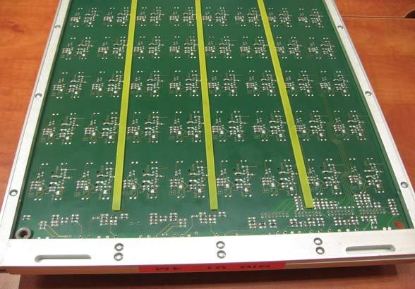
4 11.4 we had to design a board: Size: 30.7 x 11.4 = 350sq 100 pins gold edge Connector 30.7 Material: FR4, Hi-TG Industrial components Termination and P/U Resistors 2300 Controlled Impedance signals 50/100ohm
5 Outline Description of a case study: Problem definition New technology to the rescue: Embedded passive components Benefits from new technology Design flow Summary and conclusions. 5
6 Board size is 30.7 x 11.4 Very few PCB manufacturing houses would be able to handle this size. If they can, the cost would be high. Most would lack the right tooling and capabilities for manufacturing of the PCB. Even fewer assembly houses would be able to place a board of this size within the stencil, on the pick & place machines, and then through the re-flow oven. Again, cost would be an issue
7 Review of options and selection of solution The following criteria led to the selection of Embedded resistor technology: Availability of: Design tools PCB layout tools PCB manufacturers Reliability data Assembly houses An open question remains: How do we construct the Cost model?
8 Cost & Technology Resistor embedded design rules were studied in a very short time with the help of design guidelines by Ohmega-Ply. Found two sources on cost models: Source 1: CALCE Cost modeling: University of Maryland. This model is based on Assembly, Materials, Yield, Trimming, Parts procurement Parts handling, Rework
9 Cost & Technology Source 2. A model for application-specific analysis of discrete passive components P. A. Sandborn, B. Etienne, and G. Subramanian, Application-Specific Economic Analysis of Integral Passives in Printed Circuit Boards." IEEE Trans. on Electronics Packaging Manufacturing, Vol. 24, No. 3, pp , July 2001.
10 Our case study: the board, designed with Embedded resistor technology Size: 12.9 x 14.4 =185sq PCB Thickness 1.6mm Material FR4 Hi-TG 12.9 Industrial components Embedded Resistors 2300 Controlled Impedance signals 50/100ohm 14.4
11 Comparison of boards 11


12 Comparison Chart Standard Technology Embedded Technology dimension 30.7 x 11.4 = 350sq 12.9 x 14.4 = 185sq unit size layout area 100% 52% substrate 41% 16% unit cost BOM 17% 22% assembly 42% 10% 100% 48%
13 This is our case study. We considered Embedded Resistor technology Reasons being.
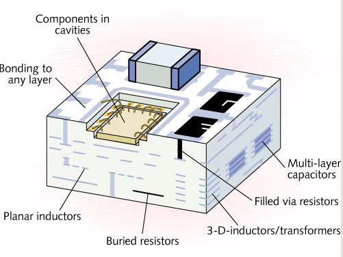
14 PCB Evolution The trend towards miniaturization has been with us for quite a while. A question that arises frequently in this context is as follows: Can we offer miniaturization in three dimensions rather than the conventional two? A positive answer to this question is now provided through the embedded passive technology.
15 PCB Evolution Passive components are known to dominate in many categories. World market share: $700B+ (2004). Passives on circuit boards occupy 40%+ of available substrate area, contain about 30% of all solder joints, take about 90% of the total assembly cost. Each IC employs additonal passive components in a typical design. Passive components have an adverse effect on the size, weight, performance and overall cost of PCBs.
16 Outline Description of a case study: Problem definition New technology to the rescue: Embedded passive components Benefits from new technology Design flow Summary and conclusions. 16

17 Benefit: Electronic Performance Improved line impedance matching Elimination of inductive reactance of SMT devices Reduced series inductance Shorter signal paths Reduced cross-talk, noise and EMI
18 Benefit: Lower resistor parasitic inductance Better functionality lower inductance from: 0.9 nhy for a1206 SMT resistor to: 0.4 nhy for an embedded resistor 18
19 Benefit: Easier PCB Layout Design Increased active component density & reduced form factors Improved wire-ability due to elimination of via and smt pads Reduced board size/ reduced layer count
20 Benefit: Lower Cost Elimination of discrete components Improved assembly yield Assembly on top side rather than on both sides Board reduced size/layer Reduced purchase cost, management, shipments Reduced storage floor area
21 Benefit: Better Quality & Reliability Fewer defects per unit (DPU) when BP is used Two fewer solder joints per discrete component Two fewer vias per discrete component Longer MTBF of an assembled board Actual values can be derived from DoD-MIL-HDBK-217 or Bellcore FR-NWT
22 Outline Description of a case study: Problem definition New technology to the rescue: Embedded passive components Benefits from new technology Design flow Summary and conclusions. 22

23 Design flow Consider BP at the Circuit Design phase, preferably earlier Define material, component technology, select design Kit(s) Analyze your design You can determine if BP is a viable option and which components should be Embedded Decide together with your PCB Manufacturer on the choice of the resistive sheet to be used in the design

24 In the process of schematic design, define naming convention for the BP and run simulation phase Design flow
25 Design flow Component selection: type, value, tolerance, power rating Embedded BOM Conventional BOM
26 Design flow Optimize component design: - p/u & p/d values -termination values Create component library Generate components minimize component area and material use

27 Design flow Design your stack-up Verify with your PCB manufacturer: feasibility, material, cost

28 Design flow Update Stack-up BOM preparation for PCB manufacture indicating: - resistor value - in what layer - what tolerance is required

29 Design flow Start Layout placement: Place main IC and components Place embedded passives in relevant layers

30 Design flow Start Routing: Connect embedded resistors Leave open plane channels Power layer route

31 Design flow GND plane: Direct connection of the embedded resistors to the plane layer


32 Design flow Gerber preparations: Superposition of GND and embedded resistor layers

33
34 Outline Description of a case study: Problem definition New technology to the rescue: Embedded passive components Benefits from new technology Design flow Summary and conclusions. 34

35 What have we gained? Smaller PCB size in production Cheaper Assembly Faster Assembly Higher Reliability Shorter Signal Traces Gained Component storage area Reduced purchase costs

36 11.4 What are the tradeoffs? Flexibility to change resistor values 30.7
37 Example (Mentor Graphics) Eliminating passives in assembly: Can resolve critical bottle necks in assembly! 200 fewer components in 5M parts/hour: 800+ days less in the assembly line! 2000 fewer components in parts/hour: 166+ days less in the assembly 24h operation!

38 Emerging Standards IPC D37A IPC D37B IPC D37C IPC D37D IPC-2316 IPC-4811 IPC-4821 Materials. IPC-4902 Embedded Passive Devices Design Task group Embedded Passive Materials Task group Embedded Passive Devices Performance Task group Embedded Passive Devices Test Methods Task group Design Guide for Embedded Passive Devices Specification for Embedded Passive Resistor Materials. Specification for Embedded Passive Capacitor Specification for Materials for Embedded Passive
39 From the National Institute of Standards and Technology (NIST): Embedded passives are seen as a key enabling technology in the National Electronics Manufacturing Initiative (NEMI) Roadmap. The technology developed in this program will translate to a variety of other applications because of the expanded performance, potential for lower system cost, reduced area requirements, and improved reliability.

40 Yet another board: I. Conventional resistors

41 II. With 2000 embedded resistors
42 THANK YOU Questions and queries are welcome Ruth Kastner ext
PI3HDMIxxx 4-Layer PCB Layout Guideline for HDMI Products
 PI3HDMIxxx 4-Layer PCB Layout Guideline for HDMI Products Introduction The differential trace impedance of HDMI is specified at 100Ω±15% in Test ID 8-8 in HDMI Compliance Test Specification Rev.1.2a and
Application-Specific Economic Analysis of Integral Passives in Printed Circuit Boards
 Application-Specific Economic Analysis of Integral Passives in Printed Circuit Boards Bevin Etienne and Peter Sandborn CALCE Electronic Products and Systems Center University of Maryland College Park,
Embedded Thin Film Resistors
 Embedded Thin Film Resistors An Update on Current Applications & Design Bruce Mahler Vice President Ohmega Technologies, Inc. IPC Designers Council Orange County Chapter July 19, 2017 NiP Thin Film Resistive
Anaren 0805 (B0809J50ATI) balun optimized for Texas Instruments CC1100/CC1101 Transceiver
 balun optimized for Texas Instruments CC1100/CC1101 Transceiver") (ANN-2005) Rev B Page 1 of 13 Anaren 0805 (B0809J50ATI) balun optimized for Texas Instruments CC1100/CC1101 Transceiver Trong N Duong RF Co-Op Nithya R Subramanian RF Engineer Introduction The tradeoff
(ANN-2005) Rev B Page 1 of 13 Anaren 0805 (B0809J50ATI) balun optimized for Texas Instruments CC1100/CC1101 Transceiver Trong N Duong RF Co-Op Nithya R Subramanian RF Engineer Introduction The tradeoff
TD-DEV V Technical Specification
 High-Efficiency MODULE Carrier Board TD-DEV-500-12V Technical Specification POWER SUPPLY TECHNOLOGY FEATURES Low profile 1U, 500W power supply High efficiency power supply Fully integrated with CPU control
Ohmega / FaradFlex 0
 Ohmega /FaradFlex 0 Introduction Growing number of PCBs with embedded passives. Driven by high frequencies and miniaturization, Embedding resistors within existing layers. Embedding capacitance between
CAD Layout Recommendations for the PowerBlox Family
 Solved by APPLICATION NOTE ANP4 TM CAD Layout Recommendations for the PowerBlox Family Introduction The Sipex PowerBlox family of parts offers designers a very high power density solution for wide input
Novel Substrate with Combined Embedded Capacitance and Resistance for Better Electrical Performance and Higher Integration
 Novel Substrate with Combined Embedded Capacitance and Resistance for Better Electrical Performance and Higher Integration John Andresakis, Pranabes Pramanik Oak-Mitsui Technologies, LLC Dan Brandler,
ABA GHz Broadband Silicon RFIC Amplifier. Application Note 1349
 ABA-52563 3.5 GHz Broadband Silicon RFIC Amplifier Application Note 1349 Introduction Avago Technologies ABA-52563 is a low current silicon gain block RFIC amplifier housed in a 6-lead SC 70 (SOT- 363)
PAGE 1/6 ISSUE Jul SERIES Micro-SPDT PART NUMBER R516 XXX 10X R 516 _ 1 0 _
 PAGE 1/6 ISSUE Jul-24-2017 SERIES Micro-SPDT PART NUMBER R516 XXX 10X R516 series: the RAMSES concept merges with the SLIM LINE technology, breaking up the frequency limits of SMT switches : - FULL SMT
APPLICATION NOTE 6381 ORGANIC LAND GRID ARRAY (OLGA) AND ITS APPLICATIONS
 AND ITS APPLICATIONS") Keywords: OLGA, SMT, PCB design APPLICATION NOTE 6381 ORGANIC LAND GRID ARRAY (OLGA) AND ITS APPLICATIONS Abstract: This application note discusses Maxim Integrated s OLGA and provides the PCB design and
Keywords: OLGA, SMT, PCB design APPLICATION NOTE 6381 ORGANIC LAND GRID ARRAY (OLGA) AND ITS APPLICATIONS Abstract: This application note discusses Maxim Integrated s OLGA and provides the PCB design and
Technology Overview. Blind Micro-vias. Embedded Resistors. Chip-on-flex. Multi-Tier Boards. RF Product. Multi-chip Modules. Embedded Capacitance
 Blind Micro-vias Embedded Resistors Multi-Tier Boards Chip-on-flex RF Product Multi-chip Modules Embedded Capacitance Technology Overview Fine-line Technology Agenda Corporate Overview Company Profile
User2User The 2007 Mentor Graphics International User Conference
 7/2/2007 1 Designing High Speed Printed Circuit Boards Using DxDesigner and Expedition Robert Navarro Jet Propulsion Laboratory, California Institute of Technology. User2User The 2007 Mentor Graphics International
TECHNICAL REPORT: CVEL Parasitic Inductance Cancellation for Filtering to Chassis Ground Using Surface Mount Capacitors
 TECHNICAL REPORT: CVEL-14-059 Parasitic Inductance Cancellation for Filtering to Chassis Ground Using Surface Mount Capacitors Andrew J. McDowell and Dr. Todd H. Hubing Clemson University April 30, 2014
PI3DPX1207B Layout Guideline. Table of Contents. 1 Layout Design Guideline Power and GROUND High-speed Signal Routing...
 PI3DPX1207B Layout Guideline Table of Contents 1 Layout Design Guideline... 2 1.1 Power and GROUND... 2 1.2 High-speed Signal Routing... 3 2 PI3DPX1207B EVB layout... 8 3 Related Reference... 8 Page 1
DESIGN FOR MANUFACTURABILITY (DFM)
") T H A N K S F O R A T T E N D I N G OUR TECHNICAL WEBINAR SERIES DESIGN FOR MANUFACTURABILITY (DFM) Presented by: We don t just sell PCBs. We sell sleep. Cirtech EDA is the exclusive SA representative
T H A N K S F O R A T T E N D I N G OUR TECHNICAL WEBINAR SERIES DESIGN FOR MANUFACTURABILITY (DFM) Presented by: We don t just sell PCBs. We sell sleep. Cirtech EDA is the exclusive SA representative
Understanding, measuring, and reducing output noise in DC/DC switching regulators
 Understanding, measuring, and reducing output noise in DC/DC switching regulators Practical tips for output noise reduction Katelyn Wiggenhorn, Applications Engineer, Buck Switching Regulators Robert Blattner,
PAGE 1/6 ISSUE SERIES Micro-SPDT PART NUMBER R516 XXX 10X. (All dimensions are in mm [inches]) R 516 _ 1 0 _
![PAGE 1/6 ISSUE SERIES Micro-SPDT PART NUMBER R516 XXX 10X. (All dimensions are in mm [inches]) R 516 _ 1 0 _](/thumbs/96/127769340.jpg "PAGE 1/6 ISSUE SERIES Micro-SPDT PART NUMBER R516 XXX 10X. (All dimensions are in mm [inches]) R 516 _ 1 0 _") PAGE 1/6 ISSUE 15-10-18 SERIES Micro-SPDT PART NUMBER R516 XXX 10X R516 series: the RAMSES concept merges with the SLIM LINE technology, breaking up the frequency limits of SMT switches : - FULL SMT TECHNOLOGY
PAGE 1/6 ISSUE 15-10-18 SERIES Micro-SPDT PART NUMBER R516 XXX 10X R516 series: the RAMSES concept merges with the SLIM LINE technology, breaking up the frequency limits of SMT switches : - FULL SMT TECHNOLOGY
Surface Mount SOT-363 (SC-70) Package. Pin Connections and Package Marking GND 1 4 V CC
 Package. Pin Connections and Package Marking GND 1 4 V CC") GHz Low Noise Silicon MMIC Amplifier Technical Data INA-63 Features Ultra-Miniature Package Internally Biased, Single 5 V Supply (12 ma) db Gain 3 db NF Unconditionally Stable Applications Amplifier for
GHz Low Noise Silicon MMIC Amplifier Technical Data INA-63 Features Ultra-Miniature Package Internally Biased, Single 5 V Supply (12 ma) db Gain 3 db NF Unconditionally Stable Applications Amplifier for
MICROELECTRONICS ASSSEMBLY TECHNOLOGIES. The QFN Platform as a Chip Packaging Foundation
 West Coast Luncheon January 15, 2014. PROMEX PROMEX INDUSTRIES INC. MICROELECTRONICS ASSSEMBLY TECHNOLOGIES The QFN Platform as a Chip Packaging Foundation 3075 Oakmead Village Drive Santa Clara CA Ɩ 95051
ECE453 Lab 5: FM Quadrature Demodulation / PCB Design Using Eagle
 ECE453 Lab 5: FM Quadrature Demodulation / PCB Design Using Eagle In this lab, you will work with your partner to design a printed circuit board for a quadrature demodulator IC and supporting components.
Antenna Matching Within an Enclosure Part II: Practical Techniques and Guidelines
 Antenna Matching Within an Enclosure Part II: Practical Techniques and Guidelines By Johnny Lienau, RF Engineer June 2012 Antenna selection and placement can be a difficult task, and the challenges of
Top View (Near-side) Side View Bottom View (Far-side) .89±.08. 4x.280. Orientation Marker Orientation Marker.
 Side View Bottom View (Far-side) .89±.08. 4x.280. Orientation Marker Orientation Marker.") Model B2F2AHF Ultra Low Profile 168 Balun Ω to 2Ω Balanced Description The B2F2AHF is a low profile sub-miniature balanced to unbalanced transformer designed for differential input locations on data conversion
Model B2F2AHF Ultra Low Profile 168 Balun Ω to 2Ω Balanced Description The B2F2AHF is a low profile sub-miniature balanced to unbalanced transformer designed for differential input locations on data conversion
Surface Mount SOT-363 (SC-70) Package. Pin Connections and Package Marking GND. V dd. Note: Package marking provides orientation and identification.
 Package. Pin Connections and Package Marking GND. V dd. Note: Package marking provides orientation and identification.") GHz V Low Current GaAs MMIC LNA Technical Data MGA-876 Features Ultra-Miniature Package.6 db Min. Noise Figure at. GHz. db Gain at. GHz Single + V or V Supply,. ma Current Applications LNA or Gain Stage
GHz V Low Current GaAs MMIC LNA Technical Data MGA-876 Features Ultra-Miniature Package.6 db Min. Noise Figure at. GHz. db Gain at. GHz Single + V or V Supply,. ma Current Applications LNA or Gain Stage
EECAD s MUST List. Requests for drawing numbers MUST be submitted via the EECAD job request form at
 Customers are required to follow certain criteria for all designs whether they are ultimately done in EECAD or by the customers themselves. These criteria, approved by EES Management, are listed below:
Hardware Design Considerations for MKW41Z/31Z/21Z BLE and IEEE Device
 NXP Semiconductors Document Number: AN5377 Application Note Rev. 2, Hardware Design Considerations for MKW41Z/31Z/21Z BLE and IEEE 802.15.4 Device 1. Introduction This application note describes Printed
PCB Fundamentals Quiz
 1. PCBs should be fabricated with layers. a. Odd Number of b. Even Number of c. Any Number of Reason: Using an odd number of layers may result in board warpage. 2. Which of the following is not taken into
AN4819 Application note
 Application note PCB design guidelines for the BlueNRG-1 device Introduction The BlueNRG1 is a very low power Bluetooth low energy (BLE) single-mode system-on-chip compliant with Bluetooth specification
Low-Cost PCB Design 1
 Low-Cost PCB Design 1 PCB design parameters Defining PCB design parameters begins with understanding: End product features, uses, environment, and lifetime goals PCB performance, manufacturing, and yield
Features. Preliminary. = +25 C, IF = 1 GHz, LO = +13 dbm*
 Typical Applications Features The is ideal for: Test Equipment & Sensors Point-to-Point Radios Point-to-Multi-Point Radios Military & Space Functional Diagram Wide IF Bandwidth: DC - 17 GHz Input IP3:
PCB Fundamentals Quiz
 1. PCBs should be fabricated with layers. a. Odd Number of b. Even Number of c. Any Number of 2. Which of the following is not taken into consideration when calculating the characteristic impedance for
Pacific Antenna Easy TR Switch
 Pacific Antenna Easy TR Switch Kit Description The Easy TR Switch is an RF sensing circuit with a double pole double throw relay that can be used to automatically switch an antenna between a separate receiver
Using Embedded Capacitance to Improve Electrical Performance, Eliminate Capacitors and Reduce Board Size in High Speed Digital and RF Applications
 Using Embedded Capacitance to Improve Electrical Performance, Eliminate Capacitors and Reduce Board Size in High Speed Digital and RF Applications Joel S. Peiffer 3M Company 3M Center, MS: 201-1E-21 St.
PCB Routing Guidelines for Signal Integrity and Power Integrity
 PCB Routing Guidelines for Signal Integrity and Power Integrity Presentation by Chris Heard Orange County chapter meeting November 18, 2015 1 Agenda Insertion Loss 101 PCB Design Guidelines For SI Simulation
Cost and production analysis for substrates with embedded passives
 Cost and production analysis for substrates with embedded passives Peter A. Sandborn, Bevin Etienne, Jeffrey W. Herrmann, Mandar M. Chincholkar Department of Mechanical Engineering University of Maryland
Application Note 1360
 ADA-4743 +17 dbm P1dB Avago Darlington Amplifier Application Note 1360 Description Avago Technologies Darlington Amplifier, ADA-4743 is a low current silicon gain block RFIC amplifier housed in a 4-lead
Pacific Antenna - Easy TR Switch
 Pacific Antenna - Easy TR Switch Kit Description The Easy TR Switch is an RF sensing switch that can be used to switch an antenna between a receiver and transmitter. It also has a second switched pair
Application Note 5011
 MGA-62563 High Performance GaAs MMIC Amplifier Application Note 511 Application Information The MGA-62563 is a high performance GaAs MMIC amplifier fabricated with Avago Technologies E-pHEMT process and
Part No. P Broadband FR4 Embedded Cellular Antenna. Low Band MHz High Band MHz
 Part No. P522304 Broadband FR4 Embedded Cellular Antenna 850 / 900 / 1800 / 1900 / 2100 MHz Supports: Broadband LTE (OCTA-BAND), LTE CAT-M, NB-IoT, SigFox, LoRa, Cellular LPWA, RPMA, Firstnet DATASHEET
IC Decoupling and EMI Suppression using X2Y Technology
 IC Decoupling and EMI Suppression using X2Y Technology Summary Decoupling and EMI suppression of ICs is a complex system level engineering problem complicated by the desire for faster switching gates,
Analog Devices Welcomes Hittite Microwave Corporation NO CONTENT ON THE ATTACHED DOCUMENT HAS CHANGED
 Analog Devices Welcomes Hittite Microwave Corporation NO CONTENT ON THE ATTACHED DOCUMENT HAS CHANGED www.analog.com www.hittite.com THIS PAGE INTENTIONALLY LEFT BLANK Typical Applications The HMC652LP2E
Design and Demonstration of a Passive, Broadband Equalizer for an SLED Chris Brinton, Matthew Wharton, and Allen Katz
 Introduction Design and Demonstration of a Passive, Broadband Equalizer for an SLED Chris Brinton, Matthew Wharton, and Allen Katz Wavelength Division Multiplexing Passive Optical Networks (WDM PONs) have
HV739 ±100V 3.0A Ultrasound Pulser Demo Board
 HV79 ±00V.0A Ultrasound Pulser Demo Board HV79DB Introduction The HV79 is a monolithic single channel, high-speed, high voltage, ultrasound transmitter pulser. This integrated, high performance circuit
Microcircuit Electrical Issues
 Microcircuit Electrical Issues Distortion The frequency at which transmitted power has dropped to 50 percent of the injected power is called the "3 db" point and is used to define the bandwidth of the
APPLICATION NOTE FOR PA.710A ANTENNA INTEGRATION
 APPLICATION NOTE FOR PA.710A ANTENNA INTEGRATION APN-11-8-001/B Page 1 of 22 1. TABLE OF CONTENTS 1. TABLE OF CONTENTS... 2 2. BASICS... 4 3. APPLICATIONS... 5 4. IMPEDANCE... 5 5. BANDWIDTH... 5 6. GAIN...
Manual Version July 2007
 Manual Version 1.2 - July 2007 Page 1 Table of Contents Section1: M3 Phono Board Build...3 Phono Board Parts List...3 Preparation...4 Fitting the Valve Bases...6 Installing the Resistors...7 Starting the
Universal Broadband FR4 Embedded LTE Antenna. Low Band MHz High Band MHz
 Part No. P822601 / P822602 Universal Broadband FR4 Embedded LTE / LPWA Antenna 700 / 750 / 850 / 900 / 1800 / 1900 / 2100 MHz Supports: Broadband LTE (OCTA-BAND), LTE CAT-M, NB-IoT, SigFox, LoRa, Cellular
Project Design for TAPR Manufacturing. Design for Manufacturability
 Project Design for TAPR Manufacturing Design for Manufacturability -or- How to ease your project into mass production with the least amount of pain (both yours and TAPR s) Scotty Cowling, WA2DFI 2010 Dayton
Mini Modules Castellation Pin Layout Guidelines - For External Antenna
 User Guide Mini Modules Castellation Pin Layout Guidelines - For External Antenna Dcoument No: 0011-00-17-03-000 (Issue B) INTRODUCTION The MeshConnect EM35x Mini Modules (ZICM35xSP0-1C and ZICM35xSP2-1C)
Low Noise Amplifier Design Methodology Summary By Ambarish Roy, Skyworks Solutions, Inc.
 February 2014 Low Noise Amplifier Design Methodology Summary By Ambarish Roy, Skyworks Solutions, Inc. Low Noise Amplifiers (LNAs) amplify weak signals received by the antenna in communication systems.
87x. MGA GHz 3 V Low Current GaAs MMIC LNA. Data Sheet
 MGA-876 GHz V Low Current GaAs MMIC LNA Data Sheet Description Avago s MGA-876 is an economical, easy-to-use GaAs MMIC amplifier that offers low noise and excellent gain for applications from to GHz. Packaged
Overcoming the Challenges of HDI Design
 ALTIUMLIVE 2018: Overcoming the Challenges of HDI Design Susy Webb Design Science Sr PCB Designer San Diego Oct, 2018 1 Challenges HDI Challenges Building the uvia structures The cost of HDI (types) boards
TMS320C6474 DDR2 Implementation Guidelines
 TMS320C6474 Implementation Guidelines Ronald Lerner... ABSTRACT This document provides implementation instructions for the interface contained on the C6474 DSP. Contents 1 Prerequisites... 2 2 C6474 Supported
= +25 C, Vcc1 = Vcc2 = Vcc3 = +5V
 v1.19 DC - 7 MHz, 1 kohm Typical Applications The is ideal for: Laser Sensor FDDI Receiver CATV FM Analog Receiver Wideband Gain Block Low Noise RF Applications Features 1 kohm Transimpedance Very Low
Sectional Design Standard for High Density Interconnect (HDI) Printed Boards
 Printed Boards") IPC-2226 ASSOCIATION CONNECTING ELECTRONICS INDUSTRIES Sectional Design Standard for High Density Interconnect (HDI) Printed Boards Developed by the HDI Design Subcommittee (D-41) of the HDI Committee
IPC-2226 ASSOCIATION CONNECTING ELECTRONICS INDUSTRIES Sectional Design Standard for High Density Interconnect (HDI) Printed Boards Developed by the HDI Design Subcommittee (D-41) of the HDI Committee
Texas Instruments DisplayPort Design Guide
 Texas Instruments DisplayPort Design Guide April 2009 1 High Speed Interface Applications Introduction This application note presents design guidelines, helping users of Texas Instruments DisplayPort devices
PAM8406 EVB User Guide
 EV Board User Guide AE Department. Revision Information PAM8406 Date Revision Description Comment 0//5 V.0 Initial Release. EV Board Schematic J5 + C C R C6 R C7 C FB FB C0 SP J4 C5 VREF 8 INL 7 6 MUTE
PCB Design Guidelines for GPS chipset designs. Section 1. Section 2. Section 3. Section 4. Section 5
 PCB Design Guidelines for GPS chipset designs The main sections of this white paper are laid out follows: Section 1 Introduction Section 2 RF Design Issues Section 3 Sirf Receiver layout guidelines Section
Application-Specific Economic Analysis of Integral Passives in Printed Circuit Boards
 Application-Specific Economic Analysis of Integral Passives in Printed Circuit Boards Peter A. Sandborn, Bevin Etienne, and Gowrishankar Subramanian CALCE Electronic Products and Systems Center University
Improve SMT Assembly Yields Using Root Cause Analysis in Stencil Design
 Improve SMT Assembly Yields Using Root Cause Analysis in Stencil Design Greg Smith FCT Assembly, Inc. gsmith@fctassembly.com This paper and presentation was first presented at the 2017 IPC Apex Expo Technical
METRIC PITCH BGA AND MICRO BGA ROUTING SOLUTIONS
 White Paper METRIC PITCH BGA AND MICRO BGA ROUTING SOLUTIONS June 2010 ABSTRACT The following paper provides Via Fanout and Trace Routing solutions for various metric pitch Ball Grid Array Packages. Note:
Improve SMT Assembly Yields Using Root Cause Analysis in Stencil Design
 Improve SMT Assembly Yields Using Root Cause Analysis in Stencil Design Greg Smith FCT Assembly, Inc. gsmith@fctassembly.com This paper and presentation was first presented at the 2017 IPC Apex Expo Technical
Top View (Near-side) Side View Bottom View (Far-side) ± ±.08. 4x.28. Orientation Marker Balanced port 1.
 Side View Bottom View (Far-side) ± ±.08. 4x.28. Orientation Marker Balanced port 1.") Model BD2FAHF Ultra Low Profile 168 Balun Ω to Ω Balanced Description The BD2FAHF is a low profile sub-miniature balanced to unbalanced transformer designed for differential input locations on data conversion
Model BD2FAHF Ultra Low Profile 168 Balun Ω to Ω Balanced Description The BD2FAHF is a low profile sub-miniature balanced to unbalanced transformer designed for differential input locations on data conversion
Features. = +25 C, Vdd = 5V, Vgg1 = Vgg2 = Open
 v3.117 HMC441LM1 Typical Applications The HMC441LM1 is a medium PA for: Point-to-Point Radios Point-to-Multi-Point Radios VSAT LO Driver for HMC Mixers Military EW & ECM Functional Diagram Vgg1, Vgg2:
GHz LOW NOISE AMPLIFIER WHM AE 1
 .. GHz LOW NOISE AMPLIFIER WHM-AE WHM-AE LNA is a low noise figure, wideband, and high linearity SMT packaged amplifier. The amplifier offers typical noise figure of.9 db and output IP of. dbm at the frequency
Application Note 5012
 MGA-61563 High Performance GaAs MMIC Amplifier Application Note 5012 Application Information The MGA-61563 is a high performance GaAs MMIC amplifier fabricated with Avago Technologies E-pHEMT process and
Design For Manufacture
 NCAB Group Seminar no. 11 Design For Manufacture NCAB GROUP Design For Manufacture Design for manufacture (DFM) What areas does DFM give consideration to? Common errors in the documentation Good design
PF3000 layout guidelines
 NXP Semiconductors Application Note Document Number: AN5094 Rev. 2.0, 7/2016 PF3000 layout guidelines 1 Introduction This document provides the best practices for the layout of the PF3000 device on printed
Design Guide for High-Speed Controlled Impedance Circuit Boards
 IPC-2141A ASSOCIATION CONNECTING ELECTRONICS INDUSTRIES Design Guide for High-Speed Controlled Impedance Circuit Boards Developed by the IPC Controlled Impedance Task Group (D-21c) of the High Speed/High
2. Design Recommendations when Using EZRadioPRO RF ICs
 EZRADIOPRO LAYOUT DESIGN GUIDE 1. Introduction The purpose of this application note is to help users design EZRadioPRO PCBs using design practices that allow for good RF performance. This application note
High Current Voltage Regulator Module (VRM) Uses DirectFET MOSFETs to Achieve Current Densities of 25A/in2 at 1MHz to Power 32-bit Servers
 Uses DirectFET MOSFETs to Achieve Current Densities of 25A/in2 at 1MHz to Power 32-bit Servers") High Current Voltage Regulator Module (VRM) Uses DirectFET MOSFETs to Achieve Current Densities of 25A/in2 at 1MHz to Power 32-bit Servers Ralph Monteiro, Carl Blake and Andrew Sawle, Arthur Woodworth
High Current Voltage Regulator Module (VRM) Uses DirectFET MOSFETs to Achieve Current Densities of 25A/in2 at 1MHz to Power 32-bit Servers Ralph Monteiro, Carl Blake and Andrew Sawle, Arthur Woodworth
MC-1010 Hardware Design Guide
 MC-1010 Hardware Design Guide Version 1.0 Date: 2013/12/31 1 General Rules for Design-in In order to obtain good GPS performances, there are some rules which require attentions for using MC-1010 GPS module.
MGA GHz 3 V, 17 dbm Amplifier. Data Sheet. Features. Description. Applications. Surface Mount Package. Simplified Schematic
 MGA-853.1 GHz 3 V, 17 dbm Amplifier Data Sheet Description Avago s MGA-853 is an economical, easy-to-use GaAs MMIC amplifier that offers excellent power and low noise figure for applications from.1 to
BOARD DESIGN, SURFACE MOUNT ASSEMBLY AND BOARD LEVEL RELIABILITY ASPECTS OF FUSIONQUAD TM PACKAGES
 BOARD DESIGN, SURFACE MOUNT ASSEMBLY AND BOARD LEVEL RELIABILITY ASPECTS OF FUSIONQUAD TM PACKAGES Ahmer Syed 1, Sundar Sethuraman 2, WonJoon Kang 1, Gary Hamming 1, YeonHo Choi 1 1 Amkor Technology, Inc.
APPLICATION NOTE FOR PA.700A ANTENNA INTEGRATION
 APPLICATION NOTE FOR PA.700A ANTENNA INTEGRATION VERSION A Your Global Source for RF, Wireless & Energy Technologies www.richardsonrfpd.com 800.737.6937 630.208.2700 APN-11-8-001/A 14-July-11 Page 1 of
Analog Devices Welcomes Hittite Microwave Corporation NO CONTENT ON THE ATTACHED DOCUMENT HAS CHANGED
 Analog Devices Welcomes Hittite Microwave Corporation NO CONTENT ON THE ATTACHED DOCUMENT HAS CHANGED www.analog.com www.hittite.com THIS PAGE INTENTIONALLY LEFT BLANK v1.14 AMPLIFIER, 18-4 GHz Typical
A passive circuit based RF optimization methodology for wireless sensor network nodes. Article (peer-reviewed)
") Title Author(s) Editor(s) A passive circuit based RF optimization methodology for wireless sensor network nodes Zheng, Liqiang; Mathewson, Alan; O'Flynn, Brendan; Hayes, Michael; Ó Mathúna, S. Cian Wu,
Title Author(s) Editor(s) A passive circuit based RF optimization methodology for wireless sensor network nodes Zheng, Liqiang; Mathewson, Alan; O'Flynn, Brendan; Hayes, Michael; Ó Mathúna, S. Cian Wu,
BGA (Ball Grid Array)
") BGA (Ball Grid Array) National Semiconductor Application Note 1126 November 2002 Table of Contents Introduction... 2 Package Overview... 3 PBGA (PLASTIC BGA) CONSTRUCTION... 3 TE-PBGA (THERMALLY ENHANCED
BGA (Ball Grid Array) National Semiconductor Application Note 1126 November 2002 Table of Contents Introduction... 2 Package Overview... 3 PBGA (PLASTIC BGA) CONSTRUCTION... 3 TE-PBGA (THERMALLY ENHANCED
Engineering White Paper The Low Mass Solution to 0402 Tombstoning
 Corporate Headquarters 2401 W. Grandview Road Phoenix, Arizona 85023 855.SUNTRON Suntroncorp.com Engineering White Paper The Low Mass Solution to 0402 Tombstoning By Eric Reno, Product Engineer II July,
Tutorial In Practical Circuit Board Design Ben LeVesque ECE480 Team 3 November 9 th, 2007
 utorial In Practical Circuit Board Design Ben LeVesque ECE480 eam 3 November 9 th, 2007 Keywords Circuit board, Cadence, Layout, Capture, post processing, trace capacity, trace ampacity, Via Abstract his
Manufacture and Performance of a Z-interconnect HDI Circuit Card Abstract Introduction
 Manufacture and Performance of a Z-interconnect HDI Circuit Card Michael Rowlands, Rabindra Das, John Lauffer, Voya Markovich EI (Endicott Interconnect Technologies) 1093 Clark Street, Endicott, NY 13760
QPI-5L. 14 Amp Active EMI Filter for 24 V DC Bus. Features. Description. Applications 查询 QPI-5L 供应商. QuietPower
 查询 5L 供应商 5L QuietPower 14 Amp Active EMI Filter for 24 V DC Bus Description The 5 active EMI filter attenuates conducted common-mode (CM) and differential-mode (DM) noise over the CISPR22 frequency range
HMC656LP2E TO HMC658LP2E v
 Typical Applications The HMC656LP2E - HMC65LP2E are ideal for: Fiber Optics Microwave Radio Military & Space Test & Measurement Scientifi c Instruments RF / Microwave Circuit Prototyping Features 3 Attenuator
3M Shielded Controlled Impedance (SCI) Latch/Eject Header 2 mm Development Kit Instructions
 Latch/Eject Header 2 mm Development Kit Instructions") 3M Shielded Controlled Impedance (SCI) Latch/Eject Header 2 mm Development Kit Instructions Contents 1.0 Purpose....................................... 1 2.0 Development Kits..................................
3M Shielded Controlled Impedance (SCI) Latch/Eject Header 2 mm Development Kit Instructions Contents 1.0 Purpose....................................... 1 2.0 Development Kits..................................
POWER designer Expert tips, tricks, and techniques for powerful designs
 POWER designer Expert tips, tricks, and techniques for powerful designs No. 114 Feature Article...1-7 High Power Density Regulators...2 Best Layout Practices for Switching Power Supplies By L. Haachitaba
APPLICATION NOTE FOR PA.710.A ANTENNA INTEGRATION
 APPLICATION NOTE FOR PA.710.A ANTENNA INTEGRATION APN-13-8-005/B/NB Page 1 of 17 1. TABLE OF CONTENTS 1. TABLE OF CONTENTS... 2 2. BASICS... 3 3. APPLICATIONS... 4 4. IMPEDANCE... 4 5. BANDWIDTH... 4 6.
Impedance Matching to 50Ω
 Impedance Matching to 50Ω The figure above shows the output matching circuit as implemented on the TRF7960EVM on a simulated Smith chart plot going from the nominal 4 Ohm TX_OUT (Pin 5) to near 50 Ohms
Application Bulletin 240
 Application Bulletin 240 Design Consideration CUSTOM CAPABILITIES Standard PC board fabrication flexibility allows for various component orientations, mounting features, and interconnect schemes. The starting
MGA GHz 3 V, 17 dbm Amplifier. Data Sheet
 MGA-853.1 GHz 3 V, 17 dbm Amplifier Data Sheet Description Avago s MGA-853 is an economical, easy-to-use GaAs MMIC amplifier that offers excellent power and low noise figure for applications from.1 to
Design for EMI & ESD compliance DESIGN FOR EMI & ESD COMPLIANCE
 DESIGN FOR EMI & ESD COMPLIANCE All of we know the causes & impacts of EMI & ESD on our boards & also on our final product. In this article, we will discuss some useful design procedures that can be followed
MAXIMUM RATINGS Note Parameter Conditions/comments Value Unit
 The CT2 Audio Volume Controls are high quality stepped 24-position attenuators. Designed for maximum sonic quality, accuracy and reliability. This makes them equally suited for audiophile and professional
--- An integrated 3D EM design flow for EM/Circuit Co-Design
 ADS users group meeting 2009 Rome 13/05, Böblingen 14-15/05, Massy 16/06 --- An integrated 3D EM design flow for EM/Circuit Co-Design Motivations and drivers for co-design Throw-The-Die-Over-The-Wall,
Application Note 58 Crystal Considerations with Dallas Real Time Clocks
 Application Note 58 Crystal Considerations with Dallas Real Time Clocks Dallas Semiconductor offers a variety of real time clocks (RTCs). The majority of these are available either as integrated circuits
MAX7036 Evaluation Kit Evaluates: MAX7036
 General Description The MAX7036 evaluation kit (EV kit) provides a proven design to evaluate the MAX7036 ASK receiver in a TQFN package with an exposed pad. The EV kit enables testing of the device s RF
Managing Complex Impedance, Isolation & Calibration for KGD RF Test Abstract
 Managing Complex Impedance, Isolation & Calibration for KGD RF Test Roger Hayward and Jeff Arasmith Cascade Microtech, Inc. Production Products Division 9100 SW Gemini Drive, Beaverton, OR 97008 503-601-1000,
RFPA5542 WLAN POWER AMPLIFIER 5 GHz WLAN PA (11a/n/ac)
") RFPA5542 WLAN POWER AMPLIFIER 5 GHz WLAN PA (11a/n/ac) Introduction This application note explains the operation of the RFPA5542 5GHz WLAN PA. The RFPA5542 is a three-stage power amplifier (PA) designed
RFPA5542 WLAN POWER AMPLIFIER 5 GHz WLAN PA (11a/n/ac) Introduction This application note explains the operation of the RFPA5542 5GHz WLAN PA. The RFPA5542 is a three-stage power amplifier (PA) designed
Model BD1631J50100AHF
 Model BD1631J51AHF Ultra Low Profile 85 Balun 5Ω to 1Ω Balanced Description The BD1631J51AHF is a low profile sub-miniature balanced to unbalanced transformer designed for differential inputs and output
PCB Design Guidelines for Reduced EMI
 PCB Design Guidelines for Reduced EMI Guided By: Prof. Ruchi Gajjar Prepared By: Shukla Jay (13MECE17) Outline Power Distribution for Two-Layer Boards Gridding Power Traces on Two-Layer Boards Ferrite
Analog Devices Welcomes Hittite Microwave Corporation NO CONTENT ON THE ATTACHED DOCUMENT HAS CHANGED
 Analog Devices Welcomes Hittite Microwave Corporation NO CONTENT ON THE ATTACHED DOCUMENT HAS CHANGED www.analog.com www.hittite.com THIS PAGE INTENTIONALLY LEFT BLANK Typical Applications Features The
RF2044 GENERAL PURPOSE AMPLIFIER
 GENERAL PURPOSE AMPLIFIER RoHS Compliant & Pb-Free Product Package Style: Micro-X Ceramic Features DC to >6000MHz Operation Internally matched Input and Output 20dB Small Signal Gain 4.0dB Noise Figure