3D Printed Electronics for Printed Circuit Structures
|
|
|
- Clifton Walsh
- 5 years ago
- Views:
Transcription
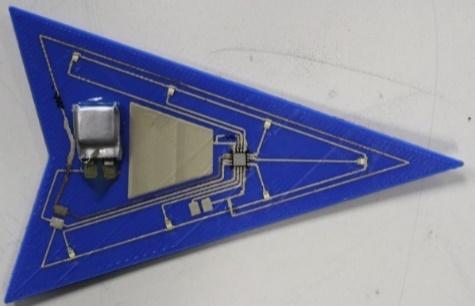
1 3D Printed Electronics for Printed Circuit Structures Samuel LeBlanc, Paul Deffenbaugh, Jacob Denkins, Kenneth Church nscrypt, Inc. Orlando, Florida Abstract Printed electronics is a familiar term that is taking on more meaning as the technology matures. Flexible electronics is sometimes referred to as a subset of this and the printing approach is one of the enabling factors for roll to roll processes. Printed electronics is improving in performance and has many applications that compete directly with printed circuit boards. The advantage of roll to roll is the speed of manufacturing, the large areas possible, and a reduction in costs. As this technology continues to mature, it is also merging with the high profile 3D printing. 3D printing is becoming more than just a rapid prototyping tool and more than just printing small plastic toys. Companies are embracing 3D printing as a manufacturing approach to fabricate complex parts that cannot be done using traditional manufacturing techniques. The combination of 3D printing and printed electronics has the potential to make novel products and more specifically making objects electrically functional. Electrically functional objects have the advantage of competing with printed circuit boards. Printed circuit structures will be a new approach to electronic packaging. It is the desire of many companies to reduce assembly processes, decrease the size of the electronics, and do this at a reduced cost. This is challenging, but the potential of printing the structure and the electronics as a single monolithic unit has many advantages. This will reduce the human touch in assembly, as the electronics and the object are printed. This will increase the ruggedness of the product, as it is a monolithic device. This will eliminate wires, solder, and connectors, making the device smaller. This has the potential to be the future of printed circuit boards and microelectronic packaging. This paper will show working demonstrations of printed circuit structures, the obstacles, and the potential future of 3D printed electronics. Introduction While 3D printing, as stereolithography (SLA), has been around since the early 1980s, it is has evolved considerably into many forms. For the purposes of this paper, fused filament deposition (FFD) also known as fused deposition modeling (FDM) will be considered. Only recently has FDM printing been joined by electronic printing to create 3D printed electronics. With this evolution in 3D printing, Printed Circuit Structures (PCS) can possess distinct advantages over Printed Circuit Boards (PCB). Many components that are present on a PCB can be integrated into a PCS. It has been shown that PCSs can contain fully embedded circuity such as antennas [1][2], lumped components [3], and even connectors [4]. Instead of creating a PCB to attach to an object, it would be possible to print the object with the circuitry as an integrated part of it. This printing method is made possible using a Direct Digital Manufacturing (DDM) machine which combines the use of multiple tool heads including a micro-dispensing pump, a heated extrusion head, a pick-and-place head, and a micro-milling, drilling, and polishing head. While PCBs require the use of many machines and require masking, PCSs can be completely automated as total fabrication is done in-situ on a single machine [5][6]. Although PCSs do have advantages, there are still several obstacles to overcome, namely speed of fabrication and strength of final parts. Fabrication Speeds FDM style 3D printing is notorious for being slow. This is mainly due to the low volumetric extrusion rates of conventional desktop 3D printers. There are many factors that determine extrusion rate. Some of these include nozzle diameter, nozzle temperature, bed temperature, X-Y movement speed, material, and even the extrusion motor. While all of these have an effect on the total amount of filament being extruded, the nozzle diameter is the main determiner of extrusion rate. Layer height, extrusion widths, and print speeds are all based on the nozzle diameter, therefore this is the facet of the printing process that stands to generate the most benefits from improving. The standard printing nozzle has a 0.4mm inside diameter. This allows for print speeds of up to mm/s, depending on machine and desired print quality. Nozzle size can be increased, however, while this can shorten the overall print time, a decrease in quality will be seen. These decreases in quality can be things such as a rougher surface finish, rounded corners, and incorrect dimensions. Larger diameter nozzles are also limited when printing small objects as the small features can be problematic. While the quality-related downsides of selecting a large diameter nozzle are not attractive, they can be dealt with. A method of printing called Spaghetti printing was developed to greatly increase extrusion rates and decrease print times. This process involves printing filament out of a specially designed 1.75mm nozzle and then utilizing a milling head to give a high-quality surface finish where required as well as bringing the print into dimension. A speed experiment was set up comparing the printing speed of an ASTM D638 Type V tensile specimen printed using a 0.4mm nozzle and the Spaghetti printing approach. Two types of tensile specimens were printed; one with a 0 infill and one with a 90 infill from the horizontal. These samples were printed with no perimeters as this would throw off tensile testing. Both of these sample types are 1.0 mm thick and were printed with a nozzle temperature of 235 C and a bed temperature of 50 C. The perimeters seen in Figure 1 and Figure 2 are used to show dimensions.


2 Figure 1: ASTM D638 Type V Tensile Specimen 0 Infill Figure 2: ASTM D638 Type V Tensile Specimen 90 Infill When printed with the 0.4 mm nozzle, each tensile specimen completed printing in 4 minutes and 24 seconds. When done with the Spaghetti method, each tensile specimen averaged 1 minute and 58 seconds total time with the actual 3D printing portion only taking 32 seconds. This experiment was repeated 25 times. Not only did the Spaghetti method complete the object more than twice as fast, the final surface finish from milling was far superior to that of the conventionally printed specimen. Figure 3: Spaghetti Printed Tensile Specimen Before and After Milling Figure 4: 0 Printed Tensile Specimen Using 0.4mm Nozzle

3 Figure 5: Micro-Dispensed Conductive Paste on 3D Printed Substrate This benefits PCS greatly as printing the electronics portions requires a smooth surface for conductive material to be dispensed. Normally, for a conductive print to be successful, the FDM substrate layer needs to be printed with a nozzle as small as 100 microns to provide a smooth surface for the conductive material to be printed accurately and true to design. Although surface mapping is available, which enables contour printing, a smooth surface is preferred. This also provides an ideal surface when printing multiple thermoplastics onto one another. Figure 6: Steps of a Printed USB Device The smooth surface enabled the level placement of a USB chip using pick-and-place. Then conductive paste was dispensed to extend the pads of the USB from the chip. Next, a polycarbonate shell was printed around the perimeter of the circular portion to form a cup for an epoxy to be dispensed. Once cured, the epoxy was milled smooth. This is a small demonstration of multi-material, multi-process in-situ PCS fabrication. Strength of Printed Parts Printable fused filaments range from somewhat durable materials such as acrylonitrile butadiene styrene (ABS) to flexible thermoplastic elastomers (TPE) and even FST-rated ULTEM. These materials have their own strengths and weaknesses. Whether it is the high impact strength of ABS or the chemical and temperature stability of ULTEM, choosing the right material for a particular application can determine whether or not it is successful. However, FDM printed parts fall well short of the strengths of other fabrication methods such as injection molding [7]. This is due to the fact that the strength of 3D printed parts rely on layer-to-layer surface adhesion, adhesion of side-by-side printed lines, and print direction as well as the mechanical properties of the material itself. Another aspect of 3D printing that decreases overall strength of printed parts compared to bulk material properties is the presence of voids that are introduced into the part during the printing process.
, voids can be observed wherever there is an overlap of side-by-side lines.")


4 Figure 7: Cross Section View of Printed Layers with a 0.4mm Nozzle Figure 8: Cross Section View of "Spaghetti" Printed Layers In both of these examples (Figure 7 and Figure 8), voids can be observed wherever there is an overlap of side-by-side lines. This is due to the fact that the edges of printed lines are rounded. To combat voids, an overlap factor can be input into the generation of the print path of the object. This will squeeze the lines closer together, minimizing voids, to an extent. When a high overlap factor is specified, the material being squeezed together must go somewhere and thus it is displaced upwards. This will create a rough surface finish if on the top layer and could throw off overall height dimensions if allowed to compound throughout the print. When printed with the 0.4mm nozzle, many, albeit smaller, voids are introduced into the object. While the few voids that are present with the Spaghetti printed layer are larger, the total void area of the parts printed with the 0.4mm nozzle is greater. These voids contribute to the ~10% difference in ultimate tensile strength for the printed specimens (Figure 9). Figure 9: UTS Comparison of "Spaghetti" and 0.4mm Nozzle Tensile Specimens The print direction plays a major role in the strength of printed parts [7][8]. It is common practice when printing structural parts to have layers printed in the direction of force that the final part will experience. To exemplify why printing in the direction of force is important, tensile specimens were printed in the direction of force (0 specimens) and perpendicular to the direction of force (90 specimens). The 0 specimens failed at an average of MPa UTS while the 90 specimens failed at a much lower force of MPa, a ~72% loss of strength. The difference in observed UTS is drastic and shows the effect that print direction has on strength. This difference is again due to the fact that since the direction of force is perpendicular to the 90 specimen s print direction, the adhesion between lines is the only thing providing resistance rather than the material itself.

5 Figure 10: UTS of 0 and 90 Tensile Specimens Ideally, there would be strength in every direction as there can be multiple directions of force in certain applications. It is common in 3D printing to not print 0 or 90 infills, but rather to print 45 as this would provide strength in multiple directions [7][8]. However, this is a compromise as this decreases the overall tensile strength when compared to printing solely in the direction of force. Furthermore, if the direction of force is in the Z-direction, the same problem arises because layer adhesion is the predominant factor in determining how much force a part can be subjected to before failure. Since layer and side-by-side line adhesion are aspects of 3D printing, there needs to be a way to increase the force they can sustain. To do this, a reflow experiment was performed. The approach was to use a temperature-controlled laser to heat and essentially reflow the already-printed plastic. A 30W laser was mounted on the machine and was placed just above the 90 tensile part. Using a non-contact thermometer, the temperature of the plastic part was elevated and held to 120 C while the laser traveled across the surface of the specimen. The laser completed three passes over the middle section of the part, reflowing the plastic and increasing the adhesion between layers. Figure 11: Laser "Reflowed" Tensile Part Tensile testing these reflowed samples yielded an average MPa UTS compared to the untreated samples average MPa UTS, a 58% increase. Figure 12: Average UTS of "Reflowed" and Untreated 90 Tensile Parts
6 While the strength increase is much improved, it is still below the UTS of parts with infill printed in the direction of force. This is important because it can enable the printing of stronger parts that exhibit force in multiple directions. While this was performed to essentially increase side-by-side line adhesion, it could also be applied to layer adhesion. By placing the laser in front of the printing head, the previous layer of deposited material would be reheated while simultaneously being printed on top of, creating a more solid part. This will increase layer adhesion with the added benefit of possibly removing voids, resulting in a stronger overall part; this is for future work. Conclusion PCBs today are optimized and ubiquitous. They can be mass produced, created relatively quickly, and are a proven, reliable product. They do have their limitations, though. They are process intensive, one-offs are not necessarily economical, and they produce a lot of waste, which creates extra expense to manufacture in the U.S. Printed circuit structures are the evolution of the PCB and 3D printing industries. They have several distinct advantages over PCB in that they greatly reduce process steps, one-offs and customization are easy because of the DDM process, and since they are primarily additive, there is very little waste. However, there are still some obstacles present. PCS as it is today would struggle with large volumes because the speeds are not yet there. Strength of fabricated parts is another obstacle in the way of PCS. 3D printed parts are not as strong as bulk properties, so consideration must be taken into the design of the PCS. Using the methods described in this paper, these two issues were addressed and improvements have been made. A more than 2x speed increase was realized through the use of Spaghetti printing which also yielded a stronger, smoother part. Another method of increasing strength utilized a laser to reflow already printed plastic creating better line-by-line and layer adhesion. Combining these methods, stronger, more durable printed circuit structures can be fabricated much faster. References [1] Deffenbaugh, Paul, et al. "Fully 3D Printed 2.4 GHz Bluetooth/Wi-Fi Antenna." International Symposium on Microelectronics. Vol No. 1. International Microelectronics Assembly and Packaging Society, [2] Nassar, Ibrahim T., et al. "A high efficiency, electrically-small, 3-D machined-substrate antenna fabricated with fused deposition modeling and 3-D printing." 2014 IEEE Radio and Wireless Symposium (RWS). IEEE, [3] Church, Kenneth H., et al. "Advanced printing for microelectronic packaging." submitted for publication in IPC APEX Expo (2014). [4] Arnal, Nicholas, et al. "3D multi-layer additive manufacturing of a 2.45 GHz RF front end." 2015 IEEE MTT-S International Microwave Symposium. IEEE, [5] Church, Kenneth H., et al. "Printed circuit structures, the evolution of printed circuit boards." IPC APEX EXPO Conference Proceedings, San Diego, CA, Feb [6] Deffenbaugh, Paul. 3D printed electromagnetic transmission and electronic structures fabricated on a single platform using advanced process integration techniques. Ph. D. dissertation, Elect. & Comput. Eng., UTEP, El Paso, TX, [7] Ahn, Sung-Hoon, et al. "Anisotropic material properties of fused deposition modeling ABS." Rapid Prototyping Journal 8.4 (2002): [8 ] Torrado, Angel R., and David A. Roberson. "Failure analysis and anisotropy evaluation of 3D-printed tensile test specimens of different geometries and print raster patterns." Journal of Failure Analysis and Prevention 16.1 (2016):
7 Printed Circuit Structures Sam LeBlanc nscrypt, Inc.
")


8 What is PCS Printed Circuit Structures (PCS) Take PCB to the 3 rd dimension Combine 3D Printing and Electronic Printing Any shape, customizable, personalized Balun Filter Antenna Feed Phase Shifter


9 Timing circuit heart Embedded timing circuit heart Micro-controller Embedded micro-controller 4 Element Phased Array Antenna Progression of Embedded USB Device


10 PCS How it is done Micro-dispensing Head 3D-Printing Head Milling Head Pick and Place Head Direct Digital Dispense 3D-Print Mill Pick and Place

11 Gantry Configuration Tool plate allows multiple heads Everything In-Situ Printing Dispensing Milling Pick and Place Curing

12 Electronic Printing Material choice Conductives Dielectrics Epoxies Adhesives Solders Conformal printing High-resolution 25μm to 3mm+


13 75μm Adhesive Dots 100μm Solder Dots Resistives Ceramic and Conductive Multi-Layer
14 3D Printing Fused Filament Deposition (FFD) Extruding thermoplastic Up to 400 C Enables higher temperature filaments Polyetheretherketon (PEEK) and Poleyetherimide (PEI) Interchangeable nozzles 12.5μm to 1.75mm

15 Direct Digital Manufacturing G-Code 3D Print object Dispense Mill Pick and Place Customization Personalization
16 Advantages In-situ fabrication Reduced labor costs Reduced time Reduced process steps Embedded Electronics Rugged, increases durability Weight Reduction More efficient use of space, no wires, connectors
17 Limitations 3D printing (FDM) is notoriously slow Higher the resolution, more time it takes Printed parts cannot match the strengths of injection molding Material selection
18 Improvements Spaghetti Printing 1.75mm Nozzle - Speed Smart slicing of objects Mill Laser Reflow


19 Milling Improved surface finish Better suited for electronic printing onto surface More suitable for RF purposes Better adhesion of materials printed onto surface Better dimensional accuracy Side View: Printed Surface Side View: Printed and Milled Surface Iso View: Printed Surface Iso View: Printed and Milled Surface

20 Milling Printed larger and milled to dimension Smooth surface finish Better dimensional accuracy Sharp features 0 and 90 print directions 0 Printed and Milled Tensile Specimen 90 Printed and Milled Tensile Specimen
21 Nozzle Choice Strength Printed in direction of force 0.4mm nozzle vs 1.75mm nozzle UTS MPa and MPa respectively 12% Increase in UTS
22 Laser Reflow Strength Printed perpendicular to direction of force 0.4mm nozzle 30W Laser used to reflow plastic 58% Increase in UTS Improved strength in multiple directions

23 Laser Reflow 30W Laser attached to gantry Driven over area of interest Real-time feedback Held at 100 C Improved interlayer adhesion 90 Tensile Specimen after Laser Reflow Non-feedback Control vs Feedback Control

 Long Pulses (1ms to CW) greater thermal loss penetration (> 500 µm) Conclusion: Need tunable pulse widths over microsecond region.")
24 Penetration Depth nm mm Pulse width effectively controls the rate at which energy/ heat is transferred to the target material. T = Absorbed Energy - Thermal Loss Heat Affected Zone short intermediate long 1 ps 1 s Pulse Duration { Thermal diffusivity Thermal conductivity Vaporization Short Pulses - (< 1 µs) limited thermal loss penetration < 500nm Intermediate Pulses (1µs to 1ms) greater thermal loss penetration (um to mm) Long Pulses (1ms to CW) greater thermal loss penetration (> 500 µm) Conclusion: Need tunable pulse widths over microsecond region. Intermediate pulse widths
25 Conclusions Spaghetti Printing: Speed 9x speed increase, optimizing, times faster Strength - ~12% increase Laser reflow - ~58% increase in strength Direct Digital Manufacturing Customizable Personalized
26 Acknowledgements US Army Sciperio US Air Force NASA University of South Florida Newton Cyberfacturing DARPA United States Navy
3D Printed Electronics for Printed Circuit Structures
 As originally published in the IPC APEX EXPO Proceedings. 3D Printed Electronics for Printed Circuit Structures Samuel LeBlanc, Paul Deffenbaugh, Jacob Denkins, Kenneth Church nscrypt, Inc. Orlando, Florida
Paul Deffenbaugh, Ph.D Senior Scientist nscrypt, Inc. Direct Digital Manufacturing: 3D Printed Electronics Enables Printed Circuit Structures
 Paul Deffenbaugh, Ph.D Senior Scientist nscrypt, Inc. Direct Digital Manufacturing: 3D Printed Electronics Enables Printed Circuit Structures sme.org/smartmfgseries Direct Digital Manufacturing: 3D Printed
Passive Direct Print Sensors
 Passive Wireless Sensor Technology Workshop June 6-7, 2012 Hyatt Regency, La Jolla, CA Passive Direct Print Sensors Mike Newton mnewton@nscrypt.com nscrypt Inc. Orlando, Florida University of Texas at
3D Printing Processes and Printing Materials
 3D Printing Processes and Printing Materials Introduction to 3D Printing Three-dimensional (3D) printing in recent years has become the main focus of public and media attention as a technology has at last
Fully 3D Printed 2.4 GHz Bluetooth/Wi-Fi Antenna
 Fully 3D Printed 2.4 GHz Bluetooth/Wi-Fi Antenna Paul Deffenbaugh, Kenneth Church The University of Texas El Paso 500 W. University Ave El Paso, TX 79968, US Ph.: 407-275-4720 Email: pdeffenbaugh@miners.utep.edu
3D Printing Technologies for Prototyping and Production
 3D Printing Technologies for Prototyping and Production HOW TO LEVERAGE ADDITIVE MANUFACTURING TO BUILD BETTER PRODUCTS ADDITIVE MANUFACTURING CNC MACHINING INJECTION MOLDING Architects don t build without
B. Flip-Chip Technology
 B. Flip-Chip Technology B1. Level 1. Introduction to Flip-Chip techniques B1.1 Why flip-chip? In the development of packaging of electronics the aim is to lower cost, increase the packaging density, improve
INCREASING INTERLAMINAR STRENGTH IN LARGE SCALE ADDITIVE MANUFACTURING
 Solid Freeform Fabrication 2018: Proceedings of the 29th Annual International Solid Freeform Fabrication Symposium An Additive Manufacturing Conference INCREASING INTERLAMINAR STRENGTH IN LARGE SCALE ADDITIVE
Design Analysis Process
 Prototype Design Analysis Process Rapid Prototyping What is rapid prototyping? A process that generates physical objects directly from geometric data without traditional tools Rapid Prototyping What is
Application Bulletin 240
 Application Bulletin 240 Design Consideration CUSTOM CAPABILITIES Standard PC board fabrication flexibility allows for various component orientations, mounting features, and interconnect schemes. The starting
PCB Supplier of the Best Quality, Lowest Price and Reliable Lead Time. Low Cost Prototype Standard Prototype & Production Stencil PCB Design
 The Best Quality PCB Supplier PCB Supplier of the Best Quality, Lowest Price Low Cost Prototype Standard Prototype & Production Stencil PCB Design Visit us: www. qualiecocircuits.co.nz OVERVIEW A thin
Direct Digital Manufacturing of Multi-layer Wideband Ku-band Patch Antennas
 University of South Florida Scholar Commons Graduate Theses and Dissertations Graduate School November 2017 Direct Digital Manufacturing of Multi-layer Wideband Ku-band Patch Antennas Merve Kacar University
3D PRINTING ON TEXTILES: TESTING OF ADHESION
 ABSTRACT 3D PRINTING ON TEXTILES: TESTING OF ADHESION Malengier B 1, Hertleer C 1, Cardon L 2, Van Langenhove L 1 (12 pt, bold) 1 Centre for Textile Science and Engineering, Department MaTCh, Ghent University,
by Ultimaker 3 Professional 3D printing made accessible
 Ultimaker 3 Professional 3D printing made accessible Complete design freedom Reliable dual extrusion with water soluble support High uptime and fast changeovers with swappable print cores Cohesive 3D printing
Prototypes on demand? Peter Arras De Nayer instituut [Hogeschool voor Wetenschap en Kunst]
![Prototypes on demand? Peter Arras De Nayer instituut [Hogeschool voor Wetenschap en Kunst]](/thumbs/78/77202330.jpg "Prototypes on demand? Peter Arras De Nayer instituut [Hogeschool voor Wetenschap en Kunst]") Prototypes on demand? Peter Arras De Nayer instituut [Hogeschool voor Wetenschap en Kunst] Pressure on time to market urges for new ways of faster prototyping. Key words: Rapid prototyping, rapid tooling,
Prototypes on demand? Peter Arras De Nayer instituut [Hogeschool voor Wetenschap en Kunst] Pressure on time to market urges for new ways of faster prototyping. Key words: Rapid prototyping, rapid tooling,
Novel Packaging Approaches for Miniature Antennas
 Novel Packaging Approaches for Miniature Antennas Will McKinzie, Greg Mendolia, and John Dutton Etenna Corporation 6100-C Frost Place, Laurel, MD 20707 wmckinzie@etenna.com, gmendolia@etenna.com, and jdutton@etenna.com
White paper. Exploring metal finishing methods for 3D-printed parts
 01 Exploring metal finishing methods for 3D-printed parts 02 Overview Method tested Centrifugal disc Centrifugal barrel Media blasting Almost all metal parts whether forged, stamped, cast, machined or
imaps New England 43rd Symposium & Expo May 03, 2016
 Digital Manufacturing and Performance Testing for Application Specific Electronic Packaging (ASEP) imaps New England 43rd Symposium & Expo May 03, 2016 Introduction Why do material choices and tight controls
CREATE PROJECT Edit Printer. Tutorial_V2 - Updated: 13,0600,1489,1629(SP6)
") CREATE PROJECT Tutorial_V2 - Updated: 13,0600,1489,1629(SP6) In this exercise, we will learn how to edit the printer! Notice/ Remember Left mouse button name is "pick" Middle mouse button name is "Exit"
CREATE PROJECT Tutorial_V2 - Updated: 13,0600,1489,1629(SP6) In this exercise, we will learn how to edit the printer! Notice/ Remember Left mouse button name is "pick" Middle mouse button name is "Exit"
3D PRINTER MATERIALS GUIDE
 3D PRINTER MATERIALS GUIDE The two primary technologies used for desktop 3D printing are fused deposition modeling () and stereolithography (). For those new to 3D printing, technology feeds melted plastic
New Lasers Improve Glass Cutting Methods
 New Lasers Improve Glass Cutting Methods Over the past decade, glass has become an increasingly sophisticated structural and functional component in uses as varied as flat panel displays (FPDs), automobiles
Reflow soldering guidelines for surface mounted power modules
 Design Note 017 Reflow soldering guidelines for surface mounted power modules Introduction Ericsson surface mounted power modules are adapted to the ever-increasing demands of high manufacturability and
High Reliability and High Temperature Application Solution Solder Joint Encapsulant Paste
 High Reliability and High Temperature Application Solution Solder Joint Encapsulant Paste YINCAE Advanced Materials, LLC WHITE PAPER October 2017 2017 YINCAE Advanced Materials, LLC - All Rights Reserved.
A Study of Direct Digital Manufactured RF/ Microwave Packaging
 University of South Florida Scholar Commons Graduate Theses and Dissertations Graduate School 10-28-2015 A Study of Direct Digital Manufactured RF/ Microwave Packaging John W.i. Stratton University of
Selective Soldering for Interconnection Technology Used in Enterprise Communication Apparatuses
 Selective Soldering for Interconnection Technology Used in Enterprise Communication Apparatuses Mark Woolley, Wesley Brown, and Dr. Jae Choi Avaya Inc. 1300 W 120 th Avenue Westminster, CO 80234 Abstract:
LARGE SCALE FUSED DEPOSITION MODELING: THE EFFECT OF PROCESSING PARAMETERS ON BEAD GEOMETRY
 Solid Freeform Fabrication 06: Proceedings of the 6th 7th Annual International Solid Freeform Fabrication Symposium An Additive Manufacturing Conference Reviewed Paper LARGE SCALE FUSED DEPOSITION MODELING:
Through Glass Via (TGV) Technology for RF Applications
 Technology for RF Applications") Through Glass Via (TGV) Technology for RF Applications C. H. Yun 1, S. Kuramochi 2, and A. B. Shorey 3 1 Qualcomm Technologies, Inc. 5775 Morehouse Dr., San Diego, California 92121, USA Ph: +1-858-651-5449,
Through Glass Via (TGV) Technology for RF Applications C. H. Yun 1, S. Kuramochi 2, and A. B. Shorey 3 1 Qualcomm Technologies, Inc. 5775 Morehouse Dr., San Diego, California 92121, USA Ph: +1-858-651-5449,
Design Guide: CNC Machining VERSION 3.4
 Design Guide: CNC Machining VERSION 3.4 CNC GUIDE V3.4 Table of Contents Overview...3 Tolerances...4 General Tolerances...4 Part Tolerances...5 Size Limitations...6 Milling...6 Lathe...6 Material Selection...7
Advanced Packaging - Pulsed-laser Heating for Flip Chip Assembly
 Page 1 of 5 Pulsed-laser Heating for Flip Chip Assembly A stress-free alternative By Thorsten Teutsch, Ph.D., Pac Tech USA, Elke Zakel, Ph.D., and Ghassem Azdasht, Pac Tech GmbH As flip chip applications
PROCEEDINGS OF SPIE. Opportunities and challenges for 3D printing of solid-state lighting systems
 PROCEEDINGS OF SPIE SPIEDigitalLibrary.org/conference-proceedings-of-spie Opportunities and challenges for 3D printing of solid-state lighting systems Nadarajah Narendran Indika U. Perera Xi Mou Dinusha
Introduction to Manufacturing Processes
 Introduction to Manufacturing Processes Products and Manufacturing Product Creation Cycle Design Material Selection Process Selection Manufacture Inspection Feedback Typical product cost breakdown Manufacturing
Bob Willis Process Guides
 What is a Printed Circuit Board Pad? What is a printed circuit board pad, it may sound like a dumb question but do you stop to think what it really does and how its size is defined and why? A printed circuit
Who we are. was born in 2006 as Spin-Off of Politecnico of Torino. Full time people employed 8. Laboratories and facilities 300 m 2
 Who we are was born in 2006 as Spin-Off of Politecnico of Torino Full time people employed 8 Laboratories and facilities 300 m 2 Administration and offices 250 m 2 Consolidated Turnover more then 600k
DIRECT METAL LASER SINTERING DESIGN GUIDE
 DIRECT METAL LASER SINTERING DESIGN GUIDE www.nextlinemfg.com TABLE OF CONTENTS Introduction... 2 What is DMLS?... 2 What is Additive Manufacturing?... 2 Typical Component of a DMLS Machine... 2 Typical
LAB 1A: Intro to SolidWorks: 2D -> 3D Brackets
 LAB 1A: Intro to SolidWorks: 2D -> 3D Brackets Set units Create Sketch Add relations Linear patterns Mirror Fillet Extrude Extrude cut First, set units. click Option on top of main menu Open Document Properties
Janice C. Booth Weapons Development and Integration Directorate Aviation and Missile Research, Development, and Engineering Center
 TECHNICAL REPORT RDMR-WD-17-30 THREE-DIMENSIONAL (3-D) PRINTED SIERPINSKI PATCH ANTENNA Janice C. Booth Weapons Development and Integration Directorate Aviation and Missile Research, Development, and Engineering
Capabilities of Flip Chip Defects Inspection Method by Using Laser Techniques
 Capabilities of Flip Chip Defects Inspection Method by Using Laser Techniques Sheng Liu and I. Charles Ume* School of Mechanical Engineering Georgia Institute of Technology Atlanta, Georgia 3332 (44) 894-7411(P)
Characterization of Printed Circuit Board Material & Manufacturing Technology for High Frequency
 As originally published in the IPC APEX EXPO Conference Proceedings. Characterization of Printed Circuit Board Material & Manufacturing Technology for High Frequency AT&S Leoben, Austria Oliver Huber 1,
Fluidic Factory Layer Offset Function
 Fluidic Factory Layer Offset Function Use of layer offset function to print on top of COC transparent substrate Application Note Page Aim & Objectives 1 Introduction 1 Layer Offset Function (Case Study)
High Efficient Heat Dissipation on Printed Circuit Boards. Markus Wille, R&D Manager, Schoeller Electronics Systems GmbH
 High Efficient Heat Dissipation on Printed Circuit Boards Markus Wille, R&D Manager, Schoeller Electronics Systems GmbH m.wille@se-pcb.de Introduction 2 Heat Flux: Q x y Q z The substrate (insulation)
Chip Assembly on MID (Molded Interconnect Device) A Path to Chip Modules with increased Functionality
 A Path to Chip Modules with increased Functionality") T e c h n o l o g y Dr. Werner Hunziker Chip Assembly on MID (Molded Interconnect Device) A Path to Chip Modules with increased Functionality The MID (Molded Interconnect Device) technology enables the
T e c h n o l o g y Dr. Werner Hunziker Chip Assembly on MID (Molded Interconnect Device) A Path to Chip Modules with increased Functionality The MID (Molded Interconnect Device) technology enables the
Visual Imaging in the Electronic Age
 Visual Imaging in the Electronic Age ART 2107, ARCH 3702, CS 1620, ENGRI 1620 3D Printing October 20, 2015 Prof. Donald P. Greenberg dpg5@cornell.edu Types of 3D Printers Selective deposition printers
Prepared by Qian Ouyang. March 2, 2013
 AN075 Rework Process for TQFN Packages Rework Process for TQFN Packages Prepared by Qian Ouyang March 2, 2013 AN075 Rev. 1.1 www.monolithicpower.com 1 ABSTRACT MPS proprietary Thin Quad Flat package No
MICROELECTRONICS ASSSEMBLY TECHNOLOGIES. The QFN Platform as a Chip Packaging Foundation
 West Coast Luncheon January 15, 2014. PROMEX PROMEX INDUSTRIES INC. MICROELECTRONICS ASSSEMBLY TECHNOLOGIES The QFN Platform as a Chip Packaging Foundation 3075 Oakmead Village Drive Santa Clara CA Ɩ 95051
Novel laser power sensor improves process control
 Novel laser power sensor improves process control A dramatic technological advancement from Coherent has yielded a completely new type of fast response power detector. The high response speed is particularly
Application Note AN-1011
 AN-1011 Board Mounting Application Note for 0.800mm Pitch Devices For part numbers IRF6100, IRF6100PBF, IR130CSP, IR130CSPPBF, IR140CSP, IR140CSPPBF, IR1H40CSP, IR1H40CSPPBF By Hazel Schofield and Philip
S e e here our newest p r o d u c ts, in c lu d in g R e p R a p F ilament!
 nonsense filament of good quality. Reducing the amount of colors available we are able to buy them in bulk reducing the price for the consumer. RepRapFilament reflects the value-seeking nature of the RepRap
Precision Prototyping THE ROLE OF 3D PRINTED MOLDS IN THE INJECTION MOLDING INDUSTRY
 By Lior Zonder, Applications Team Leader & Nadav Sella, Solutions Sales Manager, Global Field Operations INTRODUCTION Injection molding (IM) the process of injecting plastic material into a mold cavity
Features. Preliminary. = +25 C, IF = 1 GHz, LO = +13 dbm*
 Typical Applications Features The is ideal for: Test Equipment & Sensors Point-to-Point Radios Point-to-Multi-Point Radios Military & Space Functional Diagram Wide IF Bandwidth: DC - 17 GHz Input IP3:
Classification of Metal Removal Processes and Machine tools. Introduction to Manufacturing and Machining
 Classification of Metal Removal Processes and Machine tools Introduction to Manufacturing and Machining Production Engineering covers two domains: (a) Production or Manufacturing Processes (b) Production
Diverse Lasers Support Key Microelectronic Packaging Tasks
 Diverse Lasers Support Key Microelectronic Packaging Tasks Written by D Muller, R Patzel, G Oulundsen, H Halou, E Rea 23 July 2018 To support more sophisticated and compact tablets, phones, watches and
International Journal of Advance Engineering and Research Development. 3D Printing for Different Casting Patterns
 Scientific Journal of Impact Factor (SJIF): 4.72 International Journal of Advance Engineering and Research Development Volume 4, Issue 8, August -2017 3D Printing for Different Casting Patterns B.Lakshmisai
Ink-Jet Three-dimensional Printing of Photopolymers: A Method of Producing Novel Composite Materials
 Ink-Jet Three-dimensional Printing of Photopolymers: A Method of Producing Novel Composite Materials Eduardo Napadensky, Objet Geometries Ltd., Israel Current additive type manufacturing technologies such
Low Thermal Resistance Flip-Chip Bonding of 850nm 2-D VCSEL Arrays Capable of 10 Gbit/s/ch Operation
 Low Thermal Resistance Flip-Chip Bonding of 85nm -D VCSEL Arrays Capable of 1 Gbit/s/ch Operation Hendrik Roscher In 3, our well established technology of flip-chip mounted -D 85 nm backside-emitting VCSEL
Stencil Technology. Agenda: Laser Technology Stencil Materials Processes Post Process
 Stencil Technology Agenda: Laser Technology Stencil Materials Processes Post Process Laser s YAG LASER Conventional Laser Pulses Laser beam diameter is 2.3mil Ridges in the inside walls of the apertures
Selective Soldering How it has evolved to become an Integral. Method in Todays Manufacturing Processes
 2187 Selective Soldering How it has evolved to become an Integral Method in Todays Manufacturing Processes Patrick McWiggin, SolderStar s Technical Director Since regulations were bought in from the European
DESIGN AND PROCESS DEVELOPMENT FOR THE ASSEMBLY OF PASSIVE COMPONENTS
 DESIGN AND PROCESS DEVELOPMENT FOR THE ASSEMBLY OF 01005 PASSIVE COMPONENTS J. Li 1, S. Poranki 1, R. Gallardo 2, M. Abtew 2, R. Kinyanjui 2, Ph.D., and K. Srihari 1, Ph.D. 1 Watson Institute for Systems
Advanced High-Density Interconnection Technology
 Advanced High-Density Interconnection Technology Osamu Nakao 1 This report introduces Fujikura s all-polyimide IVH (interstitial Via Hole)-multi-layer circuit boards and device-embedding technology. Employing
PRECISION PROTOTYPING:
 PRECISION PROTOTYPING: THE ROLE OF 3D PRINTED MOLDS IN THE INJECTION MOLDING INDUSTRY By Lior Zonder, Applications Team Leader Nadav Sella, Solutions Sales Manager, Global Field Operations INTRODUCTION
Surface Mount RF PIN Low Distortion Attenuator Diodes. Technical Data. HSMP-381x Series and HSMP-481x Series. Features
 Surface Mount RF PIN Low Distortion Attenuator Diodes Technical Data HSMP-81x Series and HSMP-481x Series Features Diodes Optimized for: Low Distortion Attenuating Microwave Frequency Operation Surface
For rapid-prototyping and production of low volume, low cost plastic objects.
 3D Printer Standard Operating Procedure Jonathan M. Cabot 10 January 2016 For rapid-prototyping and production of low volume, low cost plastic objects. 1.0 Material Requirements 1.1 Equipment needed for
PRECISION PROTOTYPING THE ROLE OF 3D PRINTED MOLDS IN THE INJECTION MOLDING INDUSTRY
 PRECISION PROTOTYPING THE ROLE OF 3D PRINTED MOLDS IN THE INJECTION MOLDING INDUSTRY By Lior Zonder & Nadav Sella INTRODUCTION Injection molding (IM) the process of injecting plastic material into a mold
The Accuracy Myth DON T MAKE THE MISTAKE OF CONFUSING HIGH RESOLUTION WITH ACCURACY
 By Bonnie Meyer, Stratasys As additive manufacturing is called on to produce parts that do more than look good, there s a growing emphasis on dimensional accuracy and repeatability over resolution. Most
Mechanical Specifications & Ordering Part Number
 DATASHEET Part No. 1002390PT Product: Wi-Fi Tuanble PCB 5 GHz Embedded Antenna Part No. 1002390PT Wi-Fi Tunable PCB 5 GHz Embedded Antenna 5 GHz Supports: Wi-Fi applications, Agriculture, Automotive, Bluetooth,
Injection Molding from 3D Printed Molds. A study of low-volume production of small LDPE parts FORMLABS WHITE PAPER:
 FORMLABS WHITE PAPER: Injection Molding from 3D Printed Molds A study of low-volume production of small LDPE parts August 25, 2016 Formlabs and Galomb Inc. formlabs.com Table of Contents Introduction........................
Development of a Sheet-Based Material Handling System for Layered Manufacturing
 Proceedings of the 2001 IEEE International Conference on Robotics & Automation Seoul, Korea May 21-26, 2001 Development of a Sheet-Based Material Handling System for Layered Manufacturing Tao Wei, Sangeun
Print microfluidic devices in minutes for as little as $1 each.
 Print microfluidic devices in minutes for as little as $1 each www.dolomite-microfluidics.com fluidic factory» overview Fluidic Factory is the world s first commercially available 3D printer for quick
Features. = +25 C, Vdd = 5V, Vgg1 = Vgg2 = Open
 v3.117 HMC441LM1 Typical Applications The HMC441LM1 is a medium PA for: Point-to-Point Radios Point-to-Multi-Point Radios VSAT LO Driver for HMC Mixers Military EW & ECM Functional Diagram Vgg1, Vgg2:
Printed and Hybrid Integration
 Printed and Hybrid Integration Neil Chilton PhD Technical Director, Printed Electronics Limited, UK Neil.Chilton@PrintedElectronics.com Printed Electronics Limited (PEL) General Overview PEL was founded
Visual Imaging in the Electronic Age
 Visual Imaging in the Electronic Age ART 2107, ARCH 3702, CS 1620, ENGRI 1620 3D Printing November 6, 2014 Prof. Donald P. Greenberg dpg5@cornell.edu Types of 3D Printers Selective deposition printers
Chapter 2. Literature Review
 Chapter 2 Literature Review 2.1 Development of Electronic Packaging Electronic Packaging is to assemble an integrated circuit device with specific function and to connect with other electronic devices.
AN5046 Application note
 Application note Printed circuit board assembly recommendations for STMicroelectronics PowerFLAT packages Introduction The PowerFLAT package (5x6) was created to allow a larger die to fit in a standard
Make Your Ideas Matter
 Make Your Ideas Matter 3D Systems MultiJet Printing (MJP) process creates precise plastic parts that are ideal for functional prototyping, rapid tooling, and many other applications. Print rigid or flexible
STUDY OF DYNAMIC MECHANICAL PROPERTIES OF FUSED DEPOSITION MODELLING PROCESSED ULTEM MATERIAL
 American Journal of Engineering and Applied Sciences 7 (3): 307-315, 2014 ISSN: 1941-7020 2014 A. Arivazhagan et al., This open access article is distributed under a Creative Commons Attribution (CC-BY)
Micro-sensors - what happens when you make "classical" devices "small": MEMS devices and integrated bolometric IR detectors
 Micro-sensors - what happens when you make "classical" devices "small": MEMS devices and integrated bolometric IR detectors Dean P. Neikirk 1 MURI bio-ir sensors kick-off 6/16/98 Where are the targets
SOLDERABLE ANISOTROPIC CONDUCTIVE ADHESIVES FOR 3D PACKAGE APPLICATIONS
 SOLDERABLE ANISOTROPIC CONDUCTIVE ADHESIVES FOR 3D PACKAGE APPLICATIONS ABSTRACT: Dr. Mary Liu and Dr. Wusheng Yin YINCAE Advanced Materials, LLC Albany, NY 3D packaging has recently become very attractive
Per-Fix Flaw Repair Overview
 II.:::.~ chem-pak, 1Nc. Per-Fix Flaw Repair Overview Why Choose Flaw Repair Coatings Reduce scrap, eliminate rework and improve quality with Per-Fix specialty polymer flaw repair coatings. Salvage costly
60 GHz 3D integrated waveguide fed antennas using laser direct structuring
 217 11th European Conference on Antennas and Propagation (EUCAP) 6 GHz 3D integrated waveguide fed antennas using laser direct structuring technology A. Friedrich M. Fengler B. Geck D. Manteuffel Suggested
The Effects of PCB Fabrication on High-Frequency Electrical Performance
 As originally published in the IPC APEX EXPO Conference Proceedings. The Effects of PCB Fabrication on High-Frequency Electrical Performance John Coonrod, Rogers Corporation Advanced Circuit Materials
Two-component Injection Molding of Molded Interconnect Devices
 Two-component Injection Molding of Molded Interconnect Devices Jyun-yi Chen, Wen-Bin Young *1 Department of Aeronautics and Astronautics, National Cheng Kung University Tainan, 70101, Taiwan, ROC *1 youngwb@mail.ncku.edu.tw
High efficient heat dissipation on printed circuit boards
 High efficient heat dissipation on printed circuit boards Figure 1: Heat flux in a PCB Markus Wille Schoeller Electronics Systems GmbH www.schoeller-electronics.com Abstract This paper describes various
How an ink jet printer works
 How an ink jet printer works Eric Hanson Hewlett Packard Laboratories Ink jet printers are the most common type of printing devices used in home environments, and they are also frequently used personal
Investment Casting with PolyCast
 Application Note Investment Casting with PolyCast 1. Overview PolyCast is an entirely new 3D printing filament designed specifically for investment casting applications. This document provides the basic
Chapter 11 Testing, Assembly, and Packaging
 Chapter 11 Testing, Assembly, and Packaging Professor Paul K. Chu Testing The finished wafer is put on a holder and aligned for testing under a microscope Each chip on the wafer is inspected by a multiple-point
A Study of Digital RF Phase Shifters Fabricated With Additive Manufacturing
 University of South Florida Scholar Commons Graduate Theses and Dissertations Graduate School 10-30-2015 A Study of Digital RF Phase Shifters Fabricated With Additive Manufacturing Yaniel Vega University
A Miniaturized Multi-Channel TR Module Design Based on Silicon Substrate
 Progress In Electromagnetics Research Letters, Vol. 74, 117 123, 2018 A Miniaturized Multi-Channel TR Module Design Based on Silicon Substrate Jun Zhou 1, 2, *, Jiapeng Yang 1, Donglei Zhao 1, and Dongsheng
CF Series AXC5/AXC6. FEATURES 1. Vertical mating type with a 0.8 mm mated height low profile design
 For board-to-micro coaxial wire Micro coaxial connectors (Low profile) AC5/AC6 CF Series 2. with strong resistance to various environments provides high contact reliability and facilitates connection work
Assembly Instructions for SCC1XX0 series
 Technical Note 82 Assembly Instructions for SCC1XX0 series TABLE OF CONTENTS Table of Contents...1 1 Objective...2 2 VTI's 32-lead Dual In-line Package (DIL-32)...2 3 DIL-32 Package Outline and Dimensions...2
Printed Electronics and Additive Microelectronic Packaging For RF/Microwave Applications
 Printed Electronics and Additive Microelectronic Packaging For RF/Microwave Applications Prof. Craig Armiento University of Massachusetts Lowell Raytheon UMass Lowell Research Institute (RURI) Printed
3D and Aerosol Printed Conductor Dielectric Full- 3D RF Metamaterials
 3D and Aerosol Printed Conductor Dielectric Full- 3D RF Metamaterials June 22, 2017 Jimmy Hester, Evan Nguyen, Jesse Tice, and Vesna Radisic Approved for Public Release: NG17-1180, 6/2/17 Outline Introduction
Analysis of a non-symmetrical, tunable microstrip patch antenna at 60 GHz
 Analysis of a non-symmetrical, tunable microstrip patch antenna at 60 GHz Benjamin D. Horwath and Talal Al-Attar Department of Electrical Engineering, Center for Analog Design and Research Santa Clara
The Additive Manufacturing Gold Rush. Dream or Reality?
 The Additive Manufacturing Gold Rush Dream or Reality? Where s the Rush? Source: Gartner (July 2014) The Additive Manufacturing Gold Rush Tools of the Trade Additive Manufacturing (AM) Basics CAD Solid
Design Guidelines for FDM technology
 Design Guidelines for FDM technology This guideline is supposed to be used by people who already have knowledge in 3D design, CAD/CAM, etc. and it s goal is to show the key points when designing a model
The third dimension. This article is supported by...
 The Wild Format guides are intended to expand awareness and understanding of the craziness that can be created on wide format digital printing devices, from floors to lampshades and everything in between.
HOTBAR REFLOW SOLDERING
 HOTBAR REFLOW SOLDERING Content 1. Hotbar Reflow Soldering Introduction 2. Application Types 3. Process Descriptions > Flex to PCB > Wire to PCB 4. Design Guidelines 5. Equipment 6. Troubleshooting Guide
Chapter 2 High Speed Machining
 Chapter 2 High Speed Machining 1 WHAT IS HIGH SPEED MACHINING (HSM)??? Low Speed High Speed 2 Defined as the use of higher spindle speeds and axis feed rates to achieve high material removal rates without
CHAPTER 1- INTRODUCTION TO MACHINING
 CHAPTER 1- INTRODUCTION TO MACHINING LEARNING OBJECTIVES Introduction to Manufacturing, Manufacturing processes Broad classification of Manufacturing processes Kinematics elements involved in metal cutting
Assembly Instructions for SCA6x0 and SCA10x0 series
 Technical Note 71 Assembly Instructions for SCA6x0 and SCA10x0 series TABLE OF CONTENTS Table of Contents...1 1 Objective...2 2 VTI'S DIL-8 and DIL-12 packages...2 3 Package Outline and Dimensions...2
Finishing of ABS-M30 Parts Manufactured with Fused Deposition Modeling With Focus on Dimensional Accuracy. M. Fischer 1,2 ; V. Schöppner 1.
 Finishing of ABS-M3 Parts Manufactured with Fused Deposition Modeling With Focus on Dimensional Accuracy M. Fischer 1,2 ; V. Schöppner 1 1 Kunststofftechnik Paderborn (KTP), University of Paderborn, D-3312
PRODUCTION TOOLING FOR POLYMER COMPONENTS VIA THE DTM RAPIDSTEEL PROCESS
 PRODUCTION TOOLING FOR POLYMER COMPONENTS VIA THE DTM RAPIDSTEEL PROCESS KW Dalgarno, TD Stewart, & THC Childs School of Mechanical Engineering, University of Leeds, Leeds, LS2 9JT, UK Abstract This paper