PLL Group. ECE 547 project 12/19/2000. Ryan Bethel Brandon Atkinson Conrad Silvestre
|
|
|
- Theodora Jackson
- 6 years ago
- Views:
Transcription
1 PLL Group ECE 547 project 12/19/2000 Ryan Bethel Brandon Atkinson Conrad Silvestre
2 Chapter 1 Project Overview Our project was to design and layout a digital Phase lock loop. What is a PLL, you may ask? A PLL is a device that is used to regenerate a clock signal that is synchronized with the original reference signal. In other words, a PLL has one input and one output, the reference signal and the output signal, respectively. These signals should be the same frequency and at a constant phase with each other. What are these PLLs used for? Phase lock loops are used for many applications where a clock must be generated. PLLs can be used to generate a clock signal from a random binary data stream, which is convenient for systems involving wireless communications, where a synchronized clock is needed to acquire data, but the source of the signal is miles away. Digital PLLs are also used in IC designs to aid in the eradication of clock skew, the bain of any high speed system designer. Clock skew happens when a master clock drives circuitry that is relatively far away from it. When driving blocks that are different distances from the master clock, the clock pulses can arrive at different times, meaning that error can be introduced into the system. By using digital PLLs, the designer is able to minimize the effects of clock skew by using the master clock to generate the original signal, while spaced PLLs regenerate the signals for use in circuitry. What is in a PLL? A phase lock loop generally consists of three parts. The first element is the phase detector. This part of the circuit uses feedback from the output of the PLL and the reference signal input to generate a signal that represents how far away the two are from being the same. The second part of the PLL is the filter. The filter takes the output from the phase detector and makes it a signal that the last block, the VCO can use. Typical VCOs like to have signals that are very close to DC. The last block, the voltage controlled oscillator is the actual circuitry that generates the output signal. The VCO oscillates at a frequency that is dependent on the value of the filtered signal it gets from the phase detector. The output of the VCO changes as the control voltage changes, and the control voltage changes as the difference between the reference signal and VCO output changes. This feedback is what gives the PLL the ability to lock. Our project includes 2 phase detectors, an XOR and a Charge pump PFD, a few different filters, including an active lowpass, and 2 VCOs.
3 Chapter 2 Circuit Description Toplevel Organization The chip level of our PLL has several loops and several individual blocks separately bonded out. There is a PFD VCOI self contained loop as well as a PFD VCOII loop. The Active filter is bonded out directly and can be connected externally to the other blocks. There is a VCOI and a VCOII both with output buffers bonded for external connection to the bonded XOR. Although the PFD is very sensitive to capacitance and will not likely work externally connected one has been bonded out for testing purposes. There is also a pmos, an nmos, an inverter, and an output buffer bonded out for testing and characterization purposes. Phase Detectors Exclusive OR Phase Detector The exclusive OR phase detector (XORPD) was the first phase detector we used in a PLL. The XORPD Consists of a Pull up and Pull down network (PUN/PDN) of PMOS and NMOS transistors, respectively. As shown in Appendix A, the PUN consists of 2 OR logic blocks AND ed together, while the PDN consists of two AND logic blocks OR ed with each other. The result is a gate the consumes no static power, is highly symmetrical, and has negligible propagation delay in comparison to the current starved inverter. The only drawback of this circuit is that it needs to have the incoming signal and its complement. In this case the added area used for the inverters does not outweigh the effectiveness of the PD. Instance name: XORlogic Sub Instances: Inverter2 PMOS NMOS Charge Pump Phase Frequency Detector with Filter The CPPFD is a much more complicate design than the XORPD [Appendix A]. This design uses edge triggered D flip flops to detect the rising edges of the input and feedback signals, setting the HIGH_OUT line high if the input line rising edge happens first, or LOW_OUT high if the feedback rising edge happens first. The design uses a NAND gate to reset LOW_OUT and HIGH_OUT to zero when the second edge has arrived. The LOW_OUT and HIGH_OUT lines are tied into a charge pump, which is simply a current mirror with switching transistors [Appendix A]. The HIGH_OUT line is inverted and put into the switching PMOS so that if the input leads the feedback, charge is added to the capacitor at the output [Appendix A]. Conversely, if the feedback leads
4 the input, an equal amount of charge (due to the current mirror) is taken of the capacitor at the output. The major problem we had with this phase detector was that it was highly sensitive to the value of capacitance at the output node. If we had decided to use an off chip capacitance, we could probably alleviated this issue. Due to this sensitivity to capacitance, in order to mate the CPPFD designed for VCO I with VCO II, we had to change the charge pump current to compensate for the differences in gate capacitance between the two VCOs. Instance name: PFD_w_CP_and_Filt, PFD_w_CP_and_Filt_II (different resistor value) Sub Instances:PFD Charge_Pump Charge_Pump_II D Flip Flop with Active Low Clear and Set The D Flip Flop (DFF) used in the CPPFD design [Appendix A] is an edge triggered pass logic device. The active low feature is necessary for proper PFD operation, but the set feature was included in case we needed a DFF for something else. The DFF simply clocks the information on the D(ata) line to the output, unless the asyncronous clear line is low, in which case the output is zero. In the CPPFD, the D line is connected to VDD, while the CLK line is connected to the input or feedback from the VCO. This turns the DFF into a complex latch, which can be cleared at any time. The important aspect of this design is speed, so minimum sized transistors were used. Instance name: D_Flip_Flop_w_Set_Clear Sub Instances: NAND1 XGATE1 Inverter2 NAND Gate The NAND design is very similar to the XOR design. It includes a PUN and PDN, it is almost symmetrical, and its propagation delay is negligible compared to the current starved VCO. The NAND is constructed out of minimum sized NMOS and mobility corrected PMOS devices. Instance name: NAND1 Sub Instances: PMOS NMOS Transmission Gate The transmission gate (XG) [Appendix A] is a four terminal device made from two transistors; one NMOS, one PMOS. The two clock inputs are complements of each other so that both devices are either on or off. Pins A and Y are bi directional, data can flow in either direction through them. Since we are using these transmission gates in the
5 middle of a logic device, it is important that it change states quickly and that its outputs be true logic levels. Instance name: XGATE1 Sub Instances: PMOS NMOS CMOS Inverter Inverter2 [Appendix A] is a simple CMOS inverter with the PMOS width two times larger than the NMOS width to compensate for mobility difference between the two devices. This gives us a symmetrical voltage transfer characteristic for the device. The propagation delay is again not significant, since the current starved inverters delay will be much larger than this single inverter. Instance name: Inverter2 Sub Instances: PMOS NMOS VCO Circuit Description VCO Design As can be said with each element of the PLL the design of the voltage controlled oscillator is critical to the performance of the Phase Locked Loop. The initial PD chosen was the XOR. The XOR has the disadvantage of locking on signal harmonics which requires that the VCO not send any harmonics of the chosen operating frequency. The center frequency for the PLL was selected to be 10MHz. This means the VCO should operate at more than half of the center frequency(5mhz) and less than twice the center frequency(20mhz). With these constraints in mind several VCO s were considered including the Source Coupled VCO and others. The biggest downfall of most of these designs is the requirement for large capacitors and resistors using valuable silicon space. With all these considerations in mind the Current Starved Inverter VCO is chosen for this project. This design requires no capacitors or resistors. It is a transistor only design similar to the simple ring oscillator. A ring oscillator is just an odd numbered chain of inverters connected in a loop. There is no stable operating point for this circuit therefore it will oscillate at some frequency determined by the number of inverters and the propagation delay for the inverters. These ring oscillators are often used to characterize the speed of a process. In order to make a ring oscillator we must change the frequency of a ring oscillator we must change the propagation delay of the inverters. To do this we add a pmos in series with the top of the standard inverter and an nmos in series with the bottom nmos of the inverter. By selecting the proper circuit to bias the gates of these two additional transistors we can limit the current to the inverter. Since the propagation delay of the inverters in proportional to the current each inverter supplies to the output we can
6 effectively control the frequency. The gates of these two additional transistors are controlled by a current mirror where the nmos gate is driven by the VCO input control voltage. The pmos in the current mirror has its gate shorted to the drain making it active. The higher the voltage on the nmos gate the more current in the current mirror and the higher the frequency. The current mirror can be sized to give the optimum ratio of current to the inverters. VCO I The selected operating range for our VCO as stated above is 9 11MHz with a center frequency of 10MHz. Since at fmax the inverters are basically operating at their fastest. We must design the inverters to operate in our range. Mosis tests show that a 31 stage ring oscillator operates at around 104MHz. The oscillation period is roughly equivalent to the two times the propagation delay multiplied by the number of stages. This means that using minimum sized transistors would require 293 stages with a propagation delay of 155ps. This is unacceptable because it will require more space than an efficient layout. By lengthening the channels of the minimum sized transistors we can slow them down. Based on the simple RC model if we double the length of the minimum inverters channel length double the channel resistance and double the gate capacitance. Therefore doubling the channel length has the effect of increasing the propagation delay by a factor of four. For our VCO we selected a channel length of four times that of the minimum sized transistors which should slow the Ring Oscillator down to 1/8th the frequency of the Mosis ring oscillator. Therefore our 31 stage ring oscillator should have a maximum frequency of 104/8=13MHz. This is confirmed by simulation. For the design of the current mirror control circuit the pmos is sized 3 times larger than the nmos to account for the difference in the mobility of holes Vs electrons. This ratio is also repeated for the nmos and pmos inside of the inverters. The current starving transistors need to be larger than those in the inverter so that they don t greatly limit the inverters when they are hard on. For this we will make them the same width, but we will make them minimum channel length which will give them 4 times the aspect ratio of the inverter devices. Since the devices have the same width the layout will be greatly simplified. Since these devices are larger than the inverters we will ratio the current from the current mirror down to bring it within a reasonable operating range. For this we will make the transistors in the mirror eight times as big as those the current starving devices. Simulation shows that this performs as expected. VCO I: 63nmos 63pmos VCO II Although the first VCO does work in the PLL there are several drawbacks to its design. The first is that the center frequency varies with the process and cannot be adjusted externally. This is a problem because the XOR phase detector will lock on the incoming signal with some phase shift. Ideally this phase shift should be 90 degrees which will allow a clock to be generated from an incoming data stream and the data to be captured
7 on the clock edges. If the center frequency is greater or less than Vdd/2 the phase shift of the two signals varies from 90 degrees. Another problem with the first VCO is that below the threshold for the nmos the current mirror shuts off and effectively stops the oscillation all together. This makes for a very nonlinear control voltage. It is also desirable to be able to modify the operating range of the VCO for different applications. The second variation for the phase detector was selected to be a Phase Frequency Detector. This does not have the problem of locking on harmonics since it is edge triggered. For this design a more versatile VCO is also desired. All these goals can be achieved by a slight change to the inverters, the addition of three transistor and two external resistors to the VCO I design. The schematics for VCO II in Appendix A show M2, M3, and M4 added to the design. M3 and M4 form a new current mirror to drive the original mirror. The control now drives the M3 gate instead of M0 gate. This is beneficial because the input impedance of the VCO is greatly increased since only the gate of M3 is driven instead of the gates of all of the nmos starving transistors as in the first schematic. The addition of M2, which is active all the time creates a current path that is on even after M3 is cutoff. This creates a minimum frequency of oscillation for the output. By connecting two external resistors between the lower two nmos and the upper pmos it is possible to change the maximum and minimum current paths allowing for complete control over the VCO s performance. The minimum current path is chosen to be smaller than the other transistors to allow for reasonable resistor values. To take advantage of the versatility of this design we make the current starved inverters natural oscillation frequency much greater than our original design by cutting the channel lengths in half. With the selected transistors we now have a maximum frequency of around 30MHz with a short circuit for the Rfmax resistor. With a short circuit for the Rfmin resistor we have an fmin of around 13MHz and with an open circuit for Rfmin we have an fmin of 0Hz. VCO II: 65nmos 64pmos Output Buffer In order to drive an external node with our devices a buffer is required for the frequency range we are using. Assuming a 6pF load for the pins and a 14pF load for our test scope we will need to drive at least 20pF at 20MHz. Based on the simple RC model we will need a 20X buffer to drive this load. Since much of our internal PLL blocks have minimum size output stages and the VCO has a less than minimum size equivalent driving stage we have chosen to a minimum size first stage to avoid loading internal nodes. It is not possible to jump directly to a 20X stage and since we want to maintain a non inverting buffer we will use four stages(1x 5X 10X 20X). 20X Buffer: 4nmos 4pmos Filters In a Phase Lock Loop (PLL) design, the filter smoothes the output of the Phase Detector,
8 which is a train of variable duty 5 VDC pulses, prior to the signal reaching the Voltage Controlled Oscillator, which expects a slowly varying DC input. In our chip design, three filters are instanced and bonded out at the top level: a passive filter, a passive filter with phase lead correction, and an active filter. Passive Filter The simplest filter to implement is a passive filter, which consists of a series resistance and a parallel capacitance. The final version tested had a 50kΩ series resistance and a 10 pf parallel capacitance. The passive filter schematic is provided in Appendix A, Figure 1. These filters have a frequency response H(jw) = 1/(1+jwτ), where τ = RC. A theoretical Bode analysis of this filter in the Phase Lock Loop shows that the PLL is stable. When the phase delay reaches π, the gain is below unity. Instance name: Sub Instances: PllLowPass_ OTA2p Passive Filter 2 For comparison, a second passive filter is provided with a different resistance, 10kΩ instead of 50kΩ. The second passive filter schematic is provided in Appendix A, Figure 2. Instance name: Sub Instances: PllLowPass_2 OTA2p OTA10k Active Filter with Phase Lead Correction In addition to the passive filters provided, an active filter as been implemented. An active filter can be used to make a perfect time integrator, providing the VCO with a DC signal having the least ripple. However, using a perfect integrator would make the PLL unstable. A perfect integrator has a frequency response H(jw) = 1/(1+jwτ), where τ = RC This response has a phase delay of π at all frequencies. To stabilize the active filter integrator, a small resistor is added in series with the capacitance providing feedback around the active amplifier. This additional resistor adds phase lead correction. The frequency response of this modified active filter is H(jw) = (1+jwτ 1 )/jwτ 2 and has a maximum phase delay of π/2 in the frequencies of interest. The active filter design is simple. The iput from the Phase Detector goes through an inverter first. This is because the feedback around the active amplifier to the negative polarity terminal results in an inversion of the signal. An inverter corrects this inversion. After the inverter, the signal, as referenced to 2.5 Volts, is reduced in amplitude using a resistor network, so that the amplifier input is not overranged. The amplifier output is then fed back with a RC pair. The active filter schematic is provided in Appendix A.
9 Instance name: Sub Instances: PllOTAFilter OTAInverter OTAWideSing OTAVRef OTA2p OTA10k OTA100k OTA400k OTA1M Inverter The input into the active filter from the Phase Detector needs to be inverted. The filter should average the signal coming from the Phase Detector. An active filter with feedback to the negative terminal of the OTA will invert the signal around the 2.5 Volt average. To compensate for this, an inverter is inserted prior to the active filtering. The inverter schematic is given in Appendix A. Instance name: Sub Instances: OTAInverter PMOS NMOS Wide Swing Operational Transconductance Amplifier (OTA) An initial design of an active filter using a conventional Operational Amplifier did not work. At the target 10 MHz operating frequency, the gain of the conventional Operational Amplifier design was less than unity. Increasing the gain of the Operational Amplifier did not solve the problem, since the phase delay within the Operational Amplifier was sufficient to cause oscillation to occur when the gain was increased above unity. An alternate design was adopted, a Wide Swing Operational Transconductance Amplifier (OTA). This design was found to be marginally acceptable, with a gain of 12 at 10 MHz. The wide range operational transconductance amplifier schematic is given in Appendix A. Instance name: Sub Instances: OTAWideSing PMOS NMOS OTA250k OTAPdiff OTANdiff Voltage Reference A Volt Voltage Reference was provided by wiring a PMOS and NMOS transistor between Vdd and Grnd. Under heaviest load conditions, the active filter module is expected to draw no more than 10% of the current flowing through the Vref transistors
10 between Vdd and Grnd. The voltage reference schematic is given in Appendix A. Instance name: Sub Instances: OTAVRef PMOS NMOS PMOS Differential Amplifier A differential amplifier is provided with two PMOS transistors having a common source connection, two gate connections, and two drain connections. The PMOS transistors in this design were specified to be the equivalent of 60 µm wide and 5 µm long. The PMOS differential amplifier schematic is given in Appendix A. Instance name: Sub Instances: OTAPdiff PMOS NMOS Differential Amplifier A differential amplifier is provided with two NMOS transistors having a common source connection, two gate connections, and two drain connections. The NMOS transistors were specified to be the equivalent of 20 µm wide and 5 µm long. The NMOS differential amplifier schematic is given in Appendix A. Instance name: Sub Instances: OTANdiff NMOS Capacitance A single 2pF capacitance module is provided, named OTA2p. The capacitance schematic is given in Appendix A, Figures 8 through 12. Resistors For the ease of reuse, most (but not all) resistors were created in separate modules. These modules have not sub instances and are called OTA10k, OTA100k, OTA250k, OTA400k, and OTA1M. These modules have resistances of 10kΩ, 100kΩ, 250kΩ, 400kΩ, and 1 MΩ, respectively. The inverter schematic is given in Appendix A.

11 Chapter 3 Simulation Results Top Level CPPFD I and VCO I Closed loop simulation of the PLL was somewhat challenging. Although hand calculation of the filter and charge pump current values gave a ballpark estimate as to where we would lock, we had to tweak values within the simulation environment in order to get to a good lock. The pre simulation calculations were done assuming that the capacitance looking into the VCO was negligible compared to the filter capacitance. This was mistake number one. In an attempt to keep the entire loop on chip, the capacitance was scaled down to 2pF. It turned out that this capacitance was not large enough to make the gate capacitance negligible in comparison. Figure 3.1: CPPFD I and VCO I Locked in at 10MHz Above in Figure 3.1, we see the loop locked in at the center frequency of 10MHz. The markers are set on the high and low point of the oscillation after effective lock. This is the plot of the loop after the charge pump was tuned to the combined capacitance of the filter and the VCO. Before the charge pump was tuned, the control voltage oscillated around 2.5V, which is the control voltage of the VCO in lock.

12 At first, it was believed that by increasing the charge pump current by a considerable amount we could get rid of this oscillation. This was proven wrong when the opposite phenomenon happened. Increasing the charge pump current by a large amount resulted in another oscillation around the nominal lock in control voltage. This is known as over shoot. It turned out that there is a happy medium where the loop will lock. We experimented and found a region where it would lock well. Figure 3.2: CPPFD II and VCO II in Lock at 10MHz The plot above in Figure 3.2 shows CPPFD II and VCO II locked in at the center frequency. The ability of VCO II to set a maximum and minimum oscillation frequency accounts for the lower control voltage while in lock. The only difference between CPPFD I and CPPFD II is the charge pump current value. Each CPPFD is designed to work with only the corresponding VCO (CPPFD I with VCO I/ CPPFD II with VCO II).
 of the input signal.")
13 XOR With passive filter, VCO I and VCO II In order to test the functionality of the XOR phase detector with both the VCO s a passive filter was used. For this filter we chose a first order RC filter with 100k and 10pF which gives a time constant of 10 periods(1us) of the input signal. This filter is not optimized, but this allows us to confirm that the XOR and VCO blocks will function properly in a loop. The toplevel XOR VCO simulations were done using a square wave input to the XOR. The output of the XOR is feed through the RC filter and into the VCO. The output of the VCO is then feed back into the other XOR input. For a 10MHz square wave input the locking sequence is shown in Figure 3.3 below. It is evident that the initial oscillation rapidly dies out and the loop becomes locked. The blue signal is the input, the orange is the output and the red is the VCO control line. The lockin time with this setup and the passive filter is roughly 4us. This performance could be improved with optimization of the passive filter. Figure 3.3: XOR and VCO 10MHz Square Wave Lockin Once the loop gains a lock the output and the input have the same frequency with roughly a 90 degree phase shift. This is shown in Figure 3.4. Only a slight ripple exists in the VCO control signal and the input and output never lose the lock.


14 Figure 3.4: XOR and VCO 10MHz in lock In order for the PLL to function properly it must be able to track over some range of frequencies around the center frequency. To simulate the capability of the loop to lock above and below the center frequency we simulate the lock test for 9.5 and 11MHz. Although the loop may track even further once it has locked it will track at least to these extremes if it can lock on them. Figure 3.5 below shows the loop locked onto the 9.5MHz signal. For this simulation the orange is the input, the blue is the output, the green is the VCO control line and the red is the input to the RC filter. This signal does have more ripple and the phase is not 90 degrees but the loop maintains the lock. Figure 3.5: 9.5MHz Locked Signal


15 Figure 3.6 below shows the lock for 11MHz which is similar to that of the 9.5MHz above. Figure 3.6: 11MHz Locked Signal The XOR phase detector was also simulated with a second RC filter known as the Lag Filter. This filter is similar to the first passive filter with the addition of a small resistor in series with the capacitor. This resistor is only 5k ohms. This filter shows that by increasing the ripple after lockin it is possible to speed up the initial lockin time. Figure 3.7 below demonstrates this. Figure 3.7: Lag Filter

16 Phase Detectors / Logic XORlogic Simulation of the first phase detector was extremely straightforward. Propagation delay was not a significant factor, due to the long delay of the first VCO. The only real concerns with the operation of the XORPD was the output signal shape, the current driving capability, and that the logic resulted in the correct output. Figure 3.8: XORlogic into 1 mega ohm load The above simulation(figure 3.8) was run with a 20MHz square wave input into one of the XOR terminals, while the other XOR input was grounded. We ran the simulation at 20MHz because when the XOR is used in a PLL, it locks in when the input and feedback signals are 90 degrees out of phase. This means that if we lock on our center frequency of 10MHz, we will see a 20MHz pulse train at the output. We see that the shape of the output is correct. When the inputs are different, the output is high, when they are the same, the output is low. This tells us that the output will be correct at our target frequency into a 1M ohm load. We simulated the XOR with lower impedances and found that with a 100k ohm the output high and low are not exactly zero and VDD volts, but they are very close. Anything considerably below that will not have good results.
17 VCO I Simulations In order to characterize the VCO we need to get a plot of control voltage vs. frequency output. This is hard to achieve with the spectre simulation package. The best method found for performing this analysis was a parametric stepping of the input voltage in a transient analysis. Once the simulation has completed it is necessary to measure one period of each signal and calculate its frequency. These results are then compiled in to a graph(figure 3.9). C on trol V oltage VS. F req uency Frequency Control Voltage Figure 3.9: VCO I Vinput vs. Freq. Output VCO II Simulations The VCO II simulations add even more complexity than the first VCO. To plot curves for every resistor combination is impractical. The most realistic method for implementing VCO II would be for the two resistors to be implemented with the use of potentiometers. The user will measure the frequency and vary the potentiometers to gain the optimum frequency range for the application. For this it is only necessary to know the extreme values of fmin and fmax. The simulation results shown in Table 3.1 maximum and minimum values for fmin and fmax. Rfmin Rfmax Fmin(Vc=0) Fmax(Vc=5) Short Short 11.5MHz 31.25MHz Short Open 11.5MHz 12MHz Open Short 0Hz 31.25MHz Short Open 0Hz 0Hz Table 3.1: VCO II Simulation Results
charge the output capacitance when the first rising edge")
18 Charge Pump Phase Frequency Detector Simulating the CPPFD outside the loop was fairly straightforward as well. The critical factors in the design are that the CPPFD detect the rising edge of both the input and feedback signals, the CPPFD must (dis)charge the output capacitance when the first rising edge occurs and stop (dis)charging the output capacitance when the next rising edge occurs on the other input. Figure 3.10: This simulation plot shows the output of the CPPFD when two 10MHz square waves at a constant phase difference are applied at the inputs. The top graph shows the voltage over the output capacitor. We see that since there is a constant phase difference, the capacitor voltage is reduced by a constant linear rate between the rising edges on the inputs. The second graph from the top is the LOW_OUT line. This is the line that tells the charge pump to take charge off the capacitor (when it is high). Comparing the top plot and the LOW_OUT plot, we see that charge is indeed being taken of the capacitor, thereby reducing the voltage over the capacitor. The plot that is below the LOW_OUT plot is the HIGH_OUT plot. We see that there is a
19 spike in voltage on the HIGH_OUT node when LOW_OUT goes low. In reality, it is this spike that resets LOW_OUT to zero and stops the capacitor from discharging. From this simulation it is clear that the CPPFD is functioning properly. D Flip Flop with Active Low Asynchronous Set and Clear The DFF was checked qualitatively. The DFF adds little propagation delay, due to its small number of components. The major concerns with the DFF is that it displays at the output the information on D when a rising clock edge occurs, and the output waves at 10MHz are sharp. Also, for our purposes it is important that the asynchronous clear happen when CLR is low. All of these aspects were simulated. Figure 3.11: We see the output waveform at the top, while the CLR BAR line is the second plot from the top. The bottom waveform is the CLK line. We see that the output is originally high,

20 until the asynchronous clear line goes low. When the clear line is brought high again, the output stays low until the next rising clock edge. The DFF works properly. Passive Filter Simulation The DC performance of the passive filter with 50kΩ and 10pF was simulated. For an output range from 0.20 to 2.84 Volt, the input voltages must be limited to an input domain from 2.30 to 2.84 Volt. The average of the input domain is 2.57 Volt, a 2.8% deviation from the 2.5 target voltage. A unity gain simulation of the OTA showed the output to track the input voltage well over most of the 0 to 5 Volt test range. The only deviation from unity gain occurred in the top 20% of the output range. The orange line is the filtered voltage going to the VCO. The blue line is the 10 MHz reference voltage being fed into the Phase Detector. The green line is the output of the Phase Detector. The red line is the output of the VCO being fed back to the Phase Detector. The response of the passive filter was slightly underdamped. Transient simulation from a 0 Volt initial state showed an overshoot to 3.2 V at 2 µsec before settling to 2.5 V at 8 µsec. Figure 3.12 Transient simulation of passive filter module PllLowPass_ in the PLL.

21 OTA DC Simulation The DC performance of the OTA was simulated. For an output range from 0.20 to 2.84 Volt, the input voltages must be limited to an input domain from 2.30 to 2.84 Volt. The average of the input domain is 2.57 Volt, a 2.8% deviation from the 2.5 target voltage. The blue line is the output of the OTA. The green line is the voltage applied to the positive terminal of the OTA. The red line is the voltage being applied by the input/output test circuit to the negative terminal of the OTA. The orange line is the input DC voltage being applied to the input/output test circuit. Figure 3.13 DC simulation of OTA Input and Output.
22 OTA Unity Gain Simulation A unity gain simulation of the OTA showed the output to track the input voltage well over most of the 0 to 5 Volt test range. The only deviation from unity gain occurred in the top 20% of the output range. The orange line is the input DC voltage applied to the unity gain test circuit. The red line is the output from the OTA unity gain test circuit. Figure 3.14 Unity gain simulation of OTA Input and Output. OTA Filtering Simulation A transient simulation of the OTA with a feedback loop shows the successful operation of the circuit. In the example simulation shown below, the input voltage pulse train, in orange, consists of a 99% duty cycle at peak voltage and a 1% duty cycle at 0 VDC. The magnitude of the pulse train is reduced to avoid over driving the OTA. The pulse train is centered on 2.5 Volts. The filtered output voltage is shown in the blue line. Because the feedback is negative, the high input voltage results in a low output voltage. Figure 3.15 Transient simulation of the OTA active filter circuit with a 99% high duty cycle pulse train.
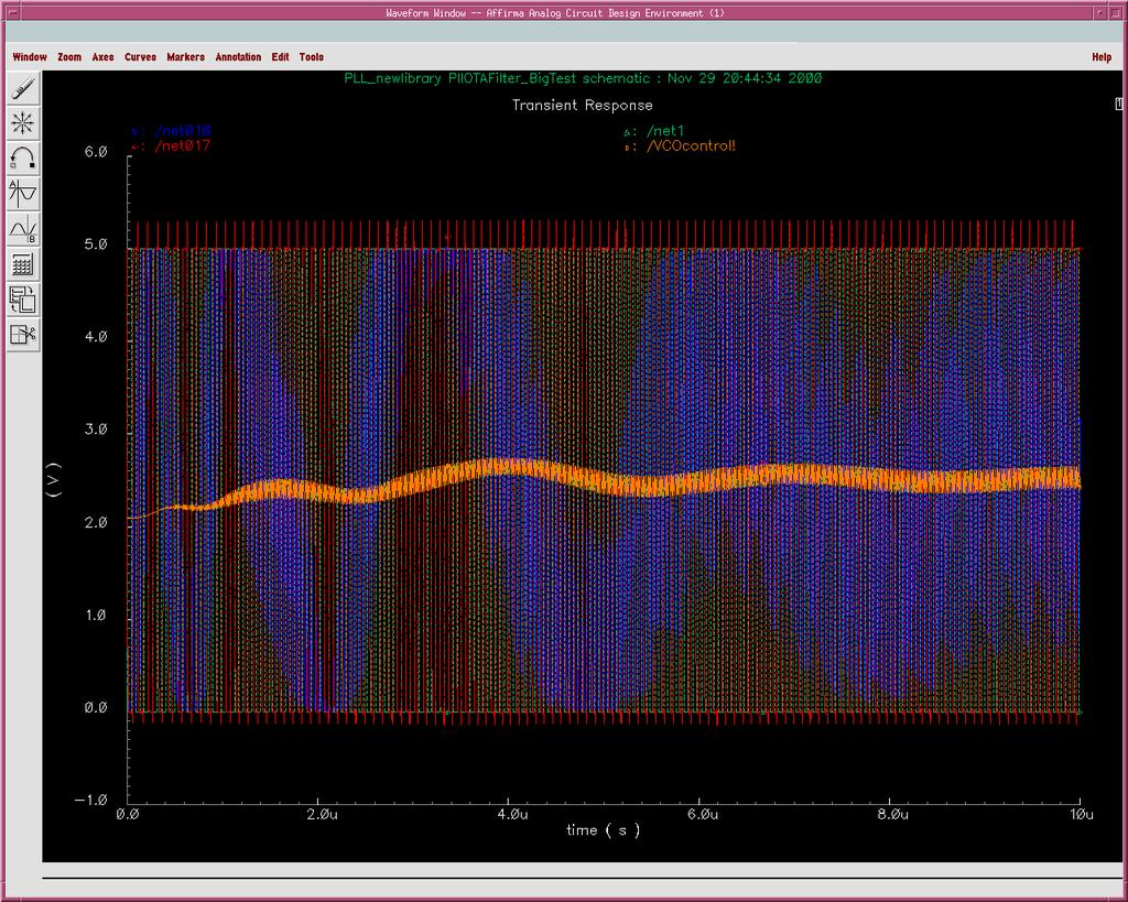
23 Pll Active Filter with Phase Lead Correction Simulation A transient simulation of the OTA filter in a PLL shows the successful operation of the circuit. In the example simulation shown below, the 10 MHz square wave being fed into the Phase Detector is shown in agree. The phase detector output is shown in blue. The OTA active filter output is shown in orange. The VCO output is shown in red. Convergence is slower than for the passive filter, taking approximately 10 µsec to converge, as opposed to the 8 µsec required by the passive filter. Figure 3.16 Convergence of the phase locking in a PLL with an active filter.
24

25 Expanded View of Converged Pll Active Filter with Phase Lead Correction Simulation A transient simulation of the OTA filter in a PLL shows the successful operation of the circuit. In the example simulation shown below, the 10 MHz square wave being fed into the Phase Detector is shown in agree. The phase detector output is shown in blue. The OTA active filter output is shown in orange. The VCO output is shown in red. Convergence is slower than for the passive filter, taking approximately 10 µsec to converge, as opposed to the 8 µsec required by the passive filter. Figure 3.17 Convergence of the phase locking in a PLL with an active filter.
26 Chapter 4 Layout Toplevel Organization In the toplevel layout the upper left corner of the layout contains the three PFD s. One is connected in a loop with VCO I, the second is connected in a loop with VCO II and the third is bonded out. The externally bonded XOR s are also in this region of the chip. The lower right corner of the chip contains the VCO I and II bonded out with output buffers. The separate output buffer is also in this corner of the chip. The lower left corner contains the active filters and passive filters. The upper right contains the pmos, nmos and inverter bonded out. The rest of the area contains metal fill in the form of a logo. Phase detectors XOR The XOR phase detector layout includes 6 NMOS, 6 PMOS and is approximately 57um x 40um [Appendix B]. CPPFD I and CPPFD II The layouts for both CPPFD s include 32 NMOS and 32 PMOS. The design dimension for both blocks is 173um x 176um. Looking at the layouts [Appendix B] with the missing corners on the lower right, we see that the only difference between the two CPPFDs is the size of the resistor (middle right). Below the resistor is the charge pump, and the capacitor can be seen above the resistor. On the left is the PFD block, which consists of a pair of D flip flops and a NAND. A guard ring surrounds the entire block to reduce noise on chip. PFD The PFD block [Figure (??) Appendix (??)] is made up of a two D flip flops connected together by a NAND gate. The PFD includes 28 NMOS and 28 PMOS transistors. The D and SET lines are connected to VDD within the PFD schematic to ensure proper operation while allowing LVS to pass on each preceding level. D Flip Flop (DFF) The DFF block [Figure (??) Appendix (??)] consists of 26 transistors, split evenly between NMOS and PMOS. There are three sub blocks in the layout, namely the inverter (inverter2), NAND (NAND1) and transmission gate (XGATE1). NAND Gate The NAND gate contains 4 transistors (2 NMOS, 2 PMOS) [Figure (??) Appendix (??)]. All of these transistors are minimum sized. Usually, we would size the PMOS transistors to have twice the width of the NMOS transistors, and then would size the series NMOS
27 transistors so that the worst case current path in the PUN and PDN are equal. It winds up that these sizing attempts cancel each other out. CMOS Inverter The CMOS inverter was thrown together, since chip area was not a limiting factor for our group [Figure (??) Appendix (??)]. The design consists of two transistors, one NMOS and one PMOS. The PMOS width was scaled to twice the width of the NMOS to correct for the mobility differences. Transmission Gate The transmission gate is made out of a single PMOS and a single NMOS. The layout of the transmission gate was also trivial since space on chip was abundant. VCO Layout VCO I Layout The layout for the first VCO is shown in Appendix??. This layout has two main sections. The ring oscillator and the control circuits. The ring oscillator is made of two rows of current starved inverters back to back. The top row has 15 and the bottom has 16 for a total of 31 stages. The top row is flipped so that the inverters can share a common nwell and vdd connection. The inverter transistors are layed out with the gates and contacts horizontal so that the gate connections for the starved devices and the gnd and vdd connections can easily be shared throughout the ring. The current mirror is located on the lefthand side of the layout with the pmos sharing the nwell for the ring oscillator. The input and output for the VCO I are both located on the lefthand side of the layout. Since the VCO is a high frequency digital block a guard ring has been added around the entire VCO block to minimize substrate noise. VCO I: 63nmos, 63pmos 176um X 49um VCO II Layout The floorplan of the VCO II layout is similar to that of the first VCO. The ring oscillator has the same basic structure except the inverters have smaller channel length. The control circuitry section is extended to accommodate the three additional transistors. The nmos devices are placed on the lower left side and the pmos shares the common nwell in the center. The VCO II block also has a guard ring around the entire block. VCO II: 65nmos, 63pmos 188um X 49um Buffer Layout
28 The layout of the Buffer was arranged to maintain a rectangular outline that could easily be incorporated in many places in the top level. A common nwell is used for the four pmos. A guard ring is also used to isolate this structure from other circuits. Buffer: 4nmos, 4pmos 55um X 34um
29 Reliability Considerations In laying out the modules used in the filter design, all interlevel connects were made with dual vias. This was done to increase the reliability of the connections, reducing the probability that a single bad connection would destroy device functionality. Passive Filter Instance name: Sub Instances: PllLowPass_ OTA2p Passive Filter With Phase Lead Correction Instance name: Sub Instances: PllLowPass_2 OTA2p OTA10k Inverter The inverted design is conventional, with instantiated PMOS and NMOS modules. Wide Swing Operational Transconductance Amplifier (OTA) Voltage Reference PMOS Differential Amplifier The layout of the differential amplifiers was designed to cancel out first order differences between paired transistors due to linear variances in process parameters across the wafer. Each PMOS transistor is broken down into twenty individual transistors. Alternating gate areas are then assigned to Transistor 1 or Transistor 2. The schematic shows five pinouts: Gate 1, Drain 1, Gate 2, Drain 2, and Common Source. In additional to the pinouts of the schematic, there is a Vdd pinout to define the voltage of the nwell and a Ground pinout for a Ground Ring. The nwell is 84 µm wide and 56 µm tall. Electrical isolation from on chip noise is provided by both the nwell isolation and the use of a guard ring around the nwell. NMOS Differential Amplifier
30 The layout of the differential amplifiers was designed to cancel out first order differences between paired transistors due to linear variances in process parameters across the wafer. Each NMOS transistor is broken down into four individual transistors. Alternating gate areas are then assigned to Transistor 1 or Transistor 2. The schematic shows five pinouts: Gate 1, Drain 1, Gate 2, Drain 2, and Common Source. In additional to the pinouts of the schematic, there is a Ground pinout for a Ground Ring. The ground ring encloses an area 45 µm wide and 42 µm tall. Electrical isolation from on chip noise is provided by the use of a guard ring. Resistor, 10kΩ The 10kΩ resistor module is a serpentine pattern 47 µm wide and 8 µm tall. The High Resistance layer of this module was designed with a 5.1 µm width. Resistor, 100kΩ The 100kΩ resistor module is a serpentine pattern 55 µm wide and 61 µm tall. High Resistance layer of this module was designed with a 5.1 µm width. The Resistor, 250kΩ The 250kΩ resistor module is a serpentine pattern 61.2 µm wide and µm tall. The High Resistance layer of this module was designed with a 5.1 µm width. Resistor, 400kΩ The 400kΩ resistor module is a serpentine pattern 123 µm wide and 103 µm tall. The High Resistance layer of this module was designed with a 5.1 µm width. This resistance is made with two separate modules, each having a 200kΩ resistance. The two modules are then connected by a Metal1 connector. This results in this module having an extra net when LVS is run. Resistor, 1 MΩ The 1MΩ resistor module is a serpentine pattern 57 µm wide and56 µm tall. Resistance layer of this module was designed with a 1.2 µm width. The High
31 Chapter 7 Conclusion The goal of this project is twofold. First to learn the tools and the process of semiconductor integrated circuit design and second to build a working PLL. We have achieved both goals to varying degrees. We have had an introduction to the Cadence IC design tools used in the industry. This has not been an in depth study of all capabilities but most aspects of the tools have been used. The process of design was also studied and followed in our PLL project. We have gone from initial designs through refinement by simulation to layout and verification. This process is is possibly the most important thing taught in this project. The tools may change but the basic challenges of layout and verification will exist in any IC design project. As for the PLL itself. We have constructed several variations beginning with basic designs and continually refining them. Several variations of each block(filter, phase detector and vco) have been included on chip to compare there performance. We have gained an understanding of the basic requirements and problems involved in designing a working PLL. This project has been very valuable.
32 Appendix A Schematics
33 Top Level Schematics
34 XOR Schematic
35 Charge Pump PFD1 Schematic
36 Charge Pump PFD 2 Schematic
37 Charge Pump 1 Schematic
38 Charge Pump 2 Schematic
39 PFD Schematic
40 NAND Schematic
41 Inverter Schematic
42 Transmission Gate Schematic
43 VCO I Schematic
44 Current Starved Inverter 4 Schematic
45 VCO II Schematic
46 Current Starved Inverter 5 Schematic
47 20X Output Buffer Schematic
48 Module OTA100k
49 Module OTA10k
50 Module OTA1M
51 Module OTA250k
52 Module OTA2p
53 Module OTA400k
54 Module OTAInverter
55 Module OTANdiff
56 Module OTAPdiff
57 Module OTAVRef
58 Module OTAWide
59 Module PllOTAFilter
60 Module PllLowPass_2
61 Module PllLowPass_
62 Appendix B Layout
63 Toplevel Layout
64 XOR Layout
65 Charge Pump PFD Layout
66 Charge Pump PFD 2 Layout
67 Charge Pump 1 Layout
68 Charge Pump 2 Layout
69 PFD Layout
70 D Flip Flop Layout
71 NAND Layout
72 Inverter Layout
73 Transmission Gate Layout
74 VCO I Layout
75 Current Starved Inverter 4
76 VCO II Layout
77 Current Starved Inverter 5
78 20X Output Buffer
79 Module PllLowPass_
80 Module PllLowPass_2
81 Module PllOTAFilter
82 Module OTAInverter
83 Module OTAWideSing
84 Module OTAVRef
85 Module OTA2p
86 Module OTA10k
87 Module OTA100k
88 Module OTA250k
89 Module OTA400k
90 Module OTA1M
91 Module OTAPdiff
92 Module OTANdiff
93 Appendix C Verification
94 Toplevel Layout Net list summary for /usr/data/ece547_fall00/pll/library/lvs/layout/netlist count 587 nets 40 terminals 51 res 14 cap 1055 pmos 959 nmos Net list summary for /usr/data/ece547_fall00/pll/library/lvs/schematic/netlist count 587 nets 45 terminals 51 res 6 cap 441 pmos 443 nmos Terminal correspondence points 1 Pin01 2 Pin02 3 Pin03 4 Pin04 5 Pin05 SIG_IN_3 6 Pin06 SIG_IN_1 7 Pin07 SIG_OUT_1 8 Pin08 SIG_IN_2 9 Pin09 SIG_OUT_2 10 Pin10 SIG_IN_2_y1 11 Pin11 SIG_IN_1_y2 12 Pin13 OTAIn 13 Pin14 OTAFeedBack 14 Pin15 OTAOut 15 Pin16 LowPass1 16 Pin17 Vref 17 Pin18 LowPass1 18 Pin19 LowPass2 19 Pin20 LowPass2 20 Pin21 21 Pin22 22 Pin23 CP_PFD_OUT 23 Pin24 VCO II_IN 24 Pin25 VCO II_OUT
95 25 Pin27 VCO II_Fmin 26 Pin28 VCO II_Fmax 27 Pin30 VCO I_OUT 28 Pin32 29 Pin33 30 Pin34 31 Pin35 32 Pin36 33 Pin37 PLL_1_Fmax 34 Pin38 PLL_1_Fmin 35 Pin40 PLL_1_out 36 Trim_1! 37 Trim_2! 38 VCOcontrol_1! 39 gnd! 40 vdd! The net lists match.
96 XOR LVS Net list summary for /usr/data/ece547_fall00/pll/library/lvs/layout/netlist count 10 nets 3 terminals 6 pmos 6 nmos Net list summary for /usr/data/ece547_fall00/pll/library/lvs/schematic/netlist count 10 nets 5 terminals 6 pmos 6 nmos Terminal correspondence points 1 L1 2 L2 3 out1 The net lists match. CPPFD 1 LVS Net list summary for /usr/data/ece547_fall00/pll/library/lvs/layout/netlist count 20 nets 5 terminals 11 res 4 pmos 4 nmos Net list summary for /usr/data/ece547_fall00/pll/library/lvs/schematic/netlist count 20 nets 5 terminals 11 res 4 pmos 4 nmos Terminal correspondence points 1 CHARGE_OUT 2 HIGH_IN 3 LOW_IN 4 gnd! 5 vdd! The net lists match.
97 CPPFD 2 LVS Net list summary for /usr/data/ece547_fall00/pll/library/lvs/layout/netlist count 22 nets 5 terminals 13 res 4 pmos 4 nmos Net list summary for /usr/data/ece547_fall00/pll/library/lvs/schematic/netlist count 22 nets 5 terminals 13 res 4 pmos 4 nmos Terminal correspondence points 1 CHARGE_OUT 2 HIGH_IN 3 LOW_IN 4 gnd! 5 vdd! The net lists match. PFD LVS Net list summary for /usr/data/ece547_fall00/pll/library/lvs/layout/netlist count 28 nets 8 terminals 28 pmos 28 nmos Net list summary for /usr/data/ece547_fall00/pll/library/lvs/schematic/netlist count 28 nets 8 terminals 28 pmos 28 nmos Terminal correspondence points 1 HIGH_OUT 2 HIGH_OUT_NOT 3 LOW_OUT 4 LOW_OUT_NOT 5 SIG_IN 6 VCO_IN 7 gnd! 8 vdd! The net lists match.
98 DFF LVS Net list summary for /usr/data/ece547_fall00/pll/library/lvs/layout/netlist count 17 nets 8 terminals 13 pmos 13 nmos Net list summary for /usr/data/ece547_fall00/pll/library/lvs/schematic/netlist count 17 nets 8 terminals 13 pmos 13 nmos Terminal correspondence points 1 CLK 2 CLR 3 D 4 Q 5 QNOT 6 SET 7 gnd! 8 vdd! The net lists match. NAND LVS Net list summary for /usr/data/ece547_fall00/pll/library/lvs/layout/netlist count 6 nets 5 terminals 2 pmos 2 nmos Net list summary for /usr/data/ece547_fall00/pll/library/lvs/schematic/netlist count 6 nets 5 terminals 2 pmos 2 nmos Terminal correspondence points 1 A 2 B 3 Y 4 gnd! 5 vdd! The net lists match.
99 Inverter LVS Net list summary for /usr/data/ece547_fall00/pll/library/lvs/layout/netlist count 4 nets 4 terminals 1 pmos 1 nmos Net list summary for /usr/data/ece547_fall00/pll/library/lvs/schematic/netlist count 4 nets 4 terminals 1 pmos 1 nmos Terminal correspondence points 1 A 2 Y 3 gnd! 4 vdd! The net lists match. XGATE LVS Net list summary for /usr/data/ece547_fall00/pll/library/lvs/layout/netlist count 6 nets 6 terminals 1 pmos 1 nmos Net list summary for /usr/data/ece547_fall00/pll/library/lvs/schematic/netlist count 6 nets 6 terminals 1 pmos 1 nmos Terminal correspondence points 1 A 2 CLK 3 CLK0 4 Y 5 gnd! 6 vdd! The net lists match.
100 VCO II LVS Net list summary for /usr/data/ece547_fall00/pll/library/lvs/layout/netlist count 100 nets 7 terminals 68 pmos 66 nmos Net list summary for /usr/data/ece547_fall00/pll/library/lvs/schematic/netlist count 100 nets 8 terminals 64 pmos 65 nmos Terminal correspondence points 1 Fmax 2 Fmin 3 Trim! 4 VC_in 5 VC_output 6 gnd! 7 vdd! The net lists match. VCOI LVS Net list summary for /usr/data/ece547_fall00/pll/library/lvs/layout/netlist count 97 nets 4 terminals 66 pmos 64 nmos Net list summary for /usr/data/ece547_fall00/pll/library/lvs/schematic/netlist count 97 nets 5 terminals 63 pmos 63 nmos
101 Terminal correspondence points 1 VC_output 2 gnd! 3 vdd! The net lists match. 20X Buffer Net list summary for /usr/data/ece547_fall00/pll/library/lvs/layout/netlist count 7 nets 4 terminals 12 pmos 9 nmos Net list summary for /usr/data/ece547_fall00/pll/library/lvs/schematic/netlist count 7 nets 4 terminals 4 pmos 4 nmos Terminal correspondence points 1 In_1X 2 Out_20X 3 gnd! 4 vdd! The net lists match.
102 Appendix D Biography of Authors
103 Ryan Bethel Ryan is an undergraduate student at the University of Maine at Orono studying Electrical Engineering. He was born in southern Maine on April 11, Ryan is a member of The Tau Beta Pi engineering honor society. He has worked as a co op at Quadic Systems semiconductor design center performing IC Layout and Simulation. Ryan is also qualified as a pilot and enjoys flying small planes. Brandon Atkinson Brandon Atkinson is a senior at the University of Maine, studying electrical engineering with a minor in mathematics. Born and raised in the small town of Hollis, Maine, he learned to appreciate the outdoors, especially on a mountain bike. His extra curricular activities include presidential duties for Eta Kappa Nu Electrical Engineering Honor Society, Tau Beta Pi functions, and helping students in the Electronics I lab. Conrad Silvestre Conrad Silvestre is currently a staff Research Engineer at the Laboratory for Surface Science and Technology at the University of Maine specializing in process engineering and electronic device fabrication technology. He has a BS in Applied Physics (California Institute of Technology, 1980), MS in Electrical Engineering (Princeton University, 1988), and a PhD in Electrical Engineering (Princeton University, 1991). His work experience includes Research Appointments at North Carolina State University ( ), the Naval Research Laboratory ( ), and a current appointment at the University of Maine ( ).
An Analog Phase-Locked Loop
 1 An Analog Phase-Locked Loop Greg Flewelling ABSTRACT This report discusses the design, simulation, and layout of an Analog Phase-Locked Loop (APLL). The circuit consists of five major parts: A differential
CHAPTER 6 PHASE LOCKED LOOP ARCHITECTURE FOR ADC
 138 CHAPTER 6 PHASE LOCKED LOOP ARCHITECTURE FOR ADC 6.1 INTRODUCTION The Clock generator is a circuit that produces the timing or the clock signal for the operation in sequential circuits. The circuit
UMAINE ECE Morse Code ROM and Transmitter at ISM Band Frequency
 UMAINE ECE Morse Code ROM and Transmitter at ISM Band Frequency Jamie E. Reinhold December 15, 2011 Abstract The design, simulation and layout of a UMAINE ECE Morse code Read Only Memory and transmitter
EE584 Introduction to VLSI Design Final Project Document Group 9 Ring Oscillator with Frequency selector
 EE584 Introduction to VLSI Design Final Project Document Group 9 Ring Oscillator with Frequency selector Group Members Uttam Kumar Boda Rajesh Tenukuntla Mohammad M Iftakhar Srikanth Yanamanagandla 1 Table
320MHz Digital Phase Lock Loop. Patrick Spinney Department of Electrical Engineering University of Maine
 320MHz Digital Phase Lock Loop Patrick Spinney Department of Electrical Engineering University of Maine December 2004 Abstract DPLLs (Digital Phase Locked Loop) are commonly used in communications systems.
Specify Gain and Phase Margins on All Your Loops
 Keywords Venable, frequency response analyzer, power supply, gain and phase margins, feedback loop, open-loop gain, output capacitance, stability margins, oscillator, power electronics circuits, voltmeter,
This chapter discusses the design issues related to the CDR architectures. The
 Chapter 2 Clock and Data Recovery Architectures 2.1 Principle of Operation This chapter discusses the design issues related to the CDR architectures. The bang-bang CDR architectures have recently found
DESIGN AND VERIFICATION OF ANALOG PHASE LOCKED LOOP CIRCUIT
 DESIGN AND VERIFICATION OF ANALOG PHASE LOCKED LOOP CIRCUIT PRADEEP G CHAGASHETTI Mr. H.V. RAVISH ARADHYA Department of E&C Department of E&C R.V.COLLEGE of ENGINEERING R.V.COLLEGE of ENGINEERING Bangalore
ASTABLE MULTIVIBRATOR
 555 TIMER ASTABLE MULTIIBRATOR MONOSTABLE MULTIIBRATOR 555 TIMER PHYSICS (LAB MANUAL) PHYSICS (LAB MANUAL) 555 TIMER Introduction The 555 timer is an integrated circuit (chip) implementing a variety of
LM13600 Dual Operational Transconductance Amplifiers with Linearizing Diodes and Buffers
 LM13600 Dual Operational Transconductance Amplifiers with Linearizing Diodes and Buffers General Description The LM13600 series consists of two current controlled transconductance amplifiers each with
10-Bit 5MHz Pipeline A/D Converter. Kannan Sockalingam and Rick Thibodeau
 10-Bit 5MHz Pipeline A/D Converter Kannan Sockalingam and Rick Thibodeau July 30, 2002 Contents 1 Introduction 8 1.1 Project Overview........................... 8 1.2 Objective...............................
Lecture 7: Components of Phase Locked Loop (PLL)
") Lecture 7: Components of Phase Locked Loop (PLL) CSCE 6933/5933 Instructor: Saraju P. Mohanty, Ph. D. NOTE: The figures, text etc included in slides are borrowed from various books, websites, authors pages,
Lecture 7: Components of Phase Locked Loop (PLL) CSCE 6933/5933 Instructor: Saraju P. Mohanty, Ph. D. NOTE: The figures, text etc included in slides are borrowed from various books, websites, authors pages,
Geared Oscillator Project Final Design Review. Nick Edwards Richard Wright
 Geared Oscillator Project Final Design Review Nick Edwards Richard Wright This paper outlines the implementation and results of a variable-rate oscillating clock supply. The circuit is designed using a
Analog CMOS Interface Circuits for UMSI Chip of Environmental Monitoring Microsystem
 Analog CMOS Interface Circuits for UMSI Chip of Environmental Monitoring Microsystem A report Submitted to Canopus Systems Inc. Zuhail Sainudeen and Navid Yazdi Arizona State University July 2001 1. Overview
Low Skew CMOS PLL Clock Drivers
 Low Skew CMOS PLL Clock Drivers The MC88915 Clock Driver utilizes phase-locked loop technology to lock its low skew outputs' frequency and phase onto an input reference clock. It is designed to provide
Testing Power Sources for Stability
 Keywords Venable, frequency response analyzer, oscillator, power source, stability testing, feedback loop, error amplifier compensation, impedance, output voltage, transfer function, gain crossover, bode
CMOS synchronous Buck switching power supply Raheel Sadiq November 28, 2016
 CMOS synchronous Buck switching power supply Raheel Sadiq November 28, 2016 Part 1: This part of the project is to lay out a bandgap. We previously built our bandgap in HW #13 which supplied a constant
NOVEMBER 28, 2016 COURSE PROJECT: CMOS SWITCHING POWER SUPPLY EE 421 DIGITAL ELECTRONICS ERIC MONAHAN
 NOVEMBER 28, 2016 COURSE PROJECT: CMOS SWITCHING POWER SUPPLY EE 421 DIGITAL ELECTRONICS ERIC MONAHAN 1.Introduction: CMOS Switching Power Supply The course design project for EE 421 Digital Engineering
CMOS Digital Integrated Circuits Lec 11 Sequential CMOS Logic Circuits
 Lec Sequential CMOS Logic Circuits Sequential Logic In Combinational Logic circuit Out Memory Sequential The output is determined by Current inputs Previous inputs Output = f(in, Previous In) The regenerative
HIGH LOW Astable multivibrators HIGH LOW 1:1
 1. Multivibrators A multivibrator circuit oscillates between a HIGH state and a LOW state producing a continuous output. Astable multivibrators generally have an even 50% duty cycle, that is that 50% of
DESIGN OF MULTIPLYING DELAY LOCKED LOOP FOR DIFFERENT MULTIPLYING FACTORS
 DESIGN OF MULTIPLYING DELAY LOCKED LOOP FOR DIFFERENT MULTIPLYING FACTORS Aman Chaudhary, Md. Imtiyaz Chowdhary, Rajib Kar Department of Electronics and Communication Engg. National Institute of Technology,
Practical Testing Techniques For Modern Control Loops
 VENABLE TECHNICAL PAPER # 16 Practical Testing Techniques For Modern Control Loops Abstract: New power supply designs are becoming harder to measure for gain margin and phase margin. This measurement is
Difference between BJTs and FETs. Junction Field Effect Transistors (JFET)
") Difference between BJTs and FETs Transistors can be categorized according to their structure, and two of the more commonly known transistor structures, are the BJT and FET. The comparison between BJTs
Difference between BJTs and FETs Transistors can be categorized according to their structure, and two of the more commonly known transistor structures, are the BJT and FET. The comparison between BJTs
Self-Biased PLL/DLL. ECG minute Final Project Presentation. Wenlan Wu Electrical and Computer Engineering University of Nevada Las Vegas
 Self-Biased PLL/DLL ECG721 60-minute Final Project Presentation Wenlan Wu Electrical and Computer Engineering University of Nevada Las Vegas Outline Motivation Self-Biasing Technique Differential Buffer
Testing and Stabilizing Feedback Loops in Today s Power Supplies
 Keywords Venable, frequency response analyzer, impedance, injection transformer, oscillator, feedback loop, Bode Plot, power supply design, open loop transfer function, voltage loop gain, error amplifier,
Capacitive Touch Sensing Tone Generator. Corey Cleveland and Eric Ponce
 Capacitive Touch Sensing Tone Generator Corey Cleveland and Eric Ponce Table of Contents Introduction Capacitive Sensing Overview Reference Oscillator Capacitive Grid Phase Detector Signal Transformer
Ultrahigh Speed Phase/Frequency Discriminator AD9901
 a FEATURES Phase and Frequency Detection ECL/TTL/CMOS Compatible Linear Transfer Function No Dead Zone MIL-STD-883 Compliant Versions Available Ultrahigh Speed Phase/Frequency Discriminator AD9901 PHASE-LOCKED
ECEN 474/704 Lab 5: Frequency Response of Inverting Amplifiers
 ECEN 474/704 Lab 5: Frequency Response of Inverting Amplifiers Objective Design, simulate and layout various inverting amplifiers. Introduction Inverting amplifiers are fundamental building blocks of electronic
DLL Based Frequency Multiplier
 DLL Based Frequency Multiplier Final Project Report VLSI Chip Design Project Project Group 4 Version 1.0 Status Reviewed Approved Ameya Bhide Ameya Bhide TSEK06 VLSI Design Project 1 of 29 Group 4 PROJECT
74VHC4046 CMOS Phase Lock Loop
 74VHC4046 CMOS Phase Lock Loop General Description The 74VHC4046 is a low power phase lock loop utilizing advanced silicon-gate CMOS technology to obtain high frequency operation both in the phase comparator
PURPOSE: NOTE: Be sure to record ALL results in your laboratory notebook.
 EE4902 Lab 9 CMOS OP-AMP PURPOSE: The purpose of this lab is to measure the closed-loop performance of an op-amp designed from individual MOSFETs. This op-amp, shown in Fig. 9-1, combines all of the major
ECEN689: Special Topics in High-Speed Links Circuits and Systems Spring 2010
 ECEN689: Special Topics in High-Speed Links Circuits and Systems Spring 010 Lecture 7: PLL Circuits Sam Palermo Analog & Mixed-Signal Center Texas A&M University Announcements Project Preliminary Report
Fractional- N PLL with 90 Phase Shift Lock and Active Switched- Capacitor Loop Filter
 J. Park, F. Maloberti: "Fractional-N PLL with 90 Phase Shift Lock and Active Switched-Capacitor Loop Filter"; Proc. of the IEEE Custom Integrated Circuits Conference, CICC 2005, San Josè, 21 September
A PROCESS AND TEMPERATURE COMPENSATED RING OSCILLATOR
 A PROCESS AND TEMPERATURE COMPENSATED RING OSCILLATOR Yang-Shyung Shyu * and Jiin-Chuan Wu Dept. of Electronics Engineering, National Chiao-Tung University 1001 Ta-Hsueh Road, Hsin-Chu, 300, Taiwan * E-mail:
A Variable-Frequency Parallel I/O Interface with Adaptive Power Supply Regulation
 WA 17.6: A Variable-Frequency Parallel I/O Interface with Adaptive Power Supply Regulation Gu-Yeon Wei, Jaeha Kim, Dean Liu, Stefanos Sidiropoulos 1, Mark Horowitz 1 Computer Systems Laboratory, Stanford
Phase-Locked Loop High-Performance Silicon-Gate CMOS
 TECHNICAL DATA Phase-Locked Loop High-Performance Silicon-Gate CMOS The device inputs are compatible with standard CMOS outputs; with pullup resistors, they are compatible with LS/ALSTTL outputs. The IN74HC4046A
ERICSSONZ LBI-30398P. MAINTENANCE MANUAL MHz PHASE LOCKED LOOP EXCITER 19D423249G1 & G2 DESCRIPTION TABLE OF CONTENTS
 MAINTENANCE MANUAL 138-174 MHz PHASE LOCKED LOOP EXCITER 19D423249G1 & G2 TABLE OF CONTENTS Page DESCRIPTION... Front Cover CIRCUIT ANALYSIS...1 MODIFICATION INSTRUCTIONS...4 PARTS LIST...5 PRODUCTION
CMOS Digital Integrated Circuits Analysis and Design
 CMOS Digital Integrated Circuits Analysis and Design Chapter 8 Sequential MOS Logic Circuits 1 Introduction Combinational logic circuit Lack the capability of storing any previous events Non-regenerative
LBI-30398N. MAINTENANCE MANUAL MHz PHASE LOCK LOOP EXCITER 19D423249G1 & G2 DESCRIPTION TABLE OF CONTENTS. Page. DESCRIPTION...
 MAINTENANCE MANUAL 138-174 MHz PHASE LOCK LOOP EXCITER 19D423249G1 & G2 LBI-30398N TABLE OF CONTENTS DESCRIPTION...Front Cover CIRCUIT ANALYSIS... 1 MODIFICATION INSTRUCTIONS... 4 PARTS LIST AND PRODUCTION
EE290C - Spring 2004 Advanced Topics in Circuit Design High-Speed Electrical Interfaces. Announcements
 EE290C - Spring 04 Advanced Topics in Circuit Design High-Speed Electrical Interfaces Lecture 11 Components Phase-Locked Loops Viterbi Decoder Borivoje Nikolic March 2, 04. Announcements Homework #2 due
CMOS Schmitt Trigger A Uniquely Versatile Design Component
 CMOS Schmitt Trigger A Uniquely Versatile Design Component INTRODUCTION The Schmitt trigger has found many applications in numerous circuits, both analog and digital. The versatility of a TTL Schmitt is
A CMOS Phase Locked Loop based PWM Generator using 90nm Technology Rajeev Pankaj Nelapati 1 B.K.Arun Teja 2 K.Sai Ravi Teja 3
 IJSRD - International Journal for Scientific Research & Development Vol. 3, Issue 06, 2015 ISSN (online): 2321-0613 A CMOS Phase Locked Loop based PWM Generator using 90nm Technology Rajeev Pankaj Nelapati
LINEAR MODELING OF A SELF-OSCILLATING PWM CONTROL LOOP
 Carl Sawtell June 2012 LINEAR MODELING OF A SELF-OSCILLATING PWM CONTROL LOOP There are well established methods of creating linearized versions of PWM control loops to analyze stability and to create
R 3 V D. V po C 1 PIN 13 PD2 OUTPUT
 MASSACHUSETTS STITUTE OF TECHNOLOGY Department of Electrical Engineering and Computer Science 6.0 Feedback Systems Spring Term 008 Issued : April, 008 PLL Design Problem Due : Friday, May 9, 008 In this
LM13700 Dual Operational Transconductance Amplifiers with Linearizing Diodes and Buffers
 LM13700 Dual Operational Transconductance Amplifiers with Linearizing Diodes and Buffers General Description The LM13700 series consists of two current controlled transconductance amplifiers, each with
EE283 Electrical Measurement Laboratory Laboratory Exercise #7: Digital Counter
 EE283 Electrical Measurement Laboratory Laboratory Exercise #7: al Counter Objectives: 1. To familiarize students with sequential digital circuits. 2. To show how digital devices can be used for measurement
9 Feedback and Control
 9 Feedback and Control Due date: Tuesday, October 20 (midnight) Reading: none An important application of analog electronics, particularly in physics research, is the servomechanical control system. Here
Computer-Based Project on VLSI Design Co 3/7
 Computer-Based Project on VLSI Design Co 3/7 Electrical Characterisation of CMOS Ring Oscillator This pamphlet describes a laboratory activity based on an integrated circuit originally designed and tested
INTEGRATED CIRCUITS. AN109 Microprocessor-compatible DACs Dec
 INTEGRATED CIRCUITS 1988 Dec DAC products are designed to convert a digital code to an analog signal. Since a common source of digital signals is the data bus of a microprocessor, DAC circuits that are
State Machine Oscillators
 by Kenneth A. Kuhn March 22, 2009, rev. March 31, 2013 Introduction State machine oscillators are based on periodic charging and discharging a capacitor to specific voltages using one or more voltage comparators
ISSN:
 507 CMOS Digital-Phase-Locked-Loop for 1 Gbit/s Clock Recovery Circuit KULDEEP THINGBAIJAM 1, CHIRAG SHARMA 2 1 Department of E&CE, Nitte Meenaskhi Institute of Technology, Yelahanka, Bangalore-560064,
Low Power, Wide Bandwidth Phase Locked Loop Design
 Low Power, Wide Bandwidth Phase Locked Loop Design Hariprasath Venkatram and Taehwan Oh Abstract A low power wide bandwidth phase locked loop is presented in the paper. The phase frequency detector, charge
Design of a Folded Cascode Operational Amplifier in a 1.2 Micron Silicon-Carbide CMOS Process
 University of Arkansas, Fayetteville ScholarWorks@UARK Electrical Engineering Undergraduate Honors Theses Electrical Engineering 5-2017 Design of a Folded Cascode Operational Amplifier in a 1.2 Micron
OPERATIONAL AMPLIFIERS (OP-AMPS) II
 II") OPERATIONAL AMPLIFIERS (OP-AMPS) II LAB 5 INTRO: INTRODUCTION TO INVERTING AMPLIFIERS AND OTHER OP-AMP CIRCUITS GOALS In this lab, you will characterize the gain and frequency dependence of inverting op-amp
OPERATIONAL AMPLIFIERS (OP-AMPS) II LAB 5 INTRO: INTRODUCTION TO INVERTING AMPLIFIERS AND OTHER OP-AMP CIRCUITS GOALS In this lab, you will characterize the gain and frequency dependence of inverting op-amp
A 24 V Chopper Offset-Stabilized Operational Amplifier with Symmetrical RC Notch Filters having sub-10 µv offset and over-120db CMRR
 ROMANIAN JOURNAL OF INFORMATION SCIENCE AND TECHNOLOGY Volume 20, Number 4, 2017, 301 312 A 24 V Chopper Offset-Stabilized Operational Amplifier with Symmetrical RC Notch Filters having sub-10 µv offset
PHASE LOCKED LOOP DESIGN
 PHASE LOCKED LOOP DESIGN by Kristen Elserougi, Ranil Fernando, Luca Wei SENIOR DESIGN PROJECT REPORT Submitted in partial fulfillment of the requirements for the degree of Bachelor of Science in Electrical
LM13700 Dual Operational Transconductance Amplifiers with Linearizing Diodes and Buffers
 LM13700 Dual Operational Transconductance Amplifiers with Linearizing Diodes and Buffers General Description The LM13700 series consists of two current controlled transconductance amplifiers, each with
ANALOG TO DIGITAL CONVERTER
 Final Project ANALOG TO DIGITAL CONVERTER As preparation for the laboratory, examine the final circuit diagram at the end of these notes and write a brief plan for the project, including a list of the
Project #3 for Electronic Circuit II
 Project #3 for Electronic Circuit II Prof. Woo-Young Choi TA: Tongsung Kim, Minkyu Kim June 1, 2015 - Deadline : 6:00 pm on June 22, 2015. Penalties for late hand-in. - Team Students are expected to form
Self Biased PLL/DLL. ECG 721 Memory Circuit Design (Spring 2017) Dane Gentry 4/17/17
 Dane Gentry 4/17/17") Self Biased PLL/DLL ECG 721 Memory Circuit Design (Spring 2017) Dane Gentry 4/17/17 1 Jitter Self Biased PLL/DLL Differential Buffer Delay Fig. 19.57 Bias Generator Self Biased DLL Input/Output p Delay
Self Biased PLL/DLL ECG 721 Memory Circuit Design (Spring 2017) Dane Gentry 4/17/17 1 Jitter Self Biased PLL/DLL Differential Buffer Delay Fig. 19.57 Bias Generator Self Biased DLL Input/Output p Delay
New Techniques for Testing Power Factor Correction Circuits
 Keywords Venable, frequency response analyzer, impedance, injection transformer, oscillator, feedback loop, Bode Plot, power supply design, power factor correction circuits, current mode control, gain
EE584 (Fall 2006) Introduction to VLSI CAD Project. Design of Ring Oscillator using NOR gates
 Introduction to VLSI CAD Project. Design of Ring Oscillator using NOR gates") EE584 (Fall 2006) Introduction to VLSI CAD Project Design of Ring Oscillator using NOR gates By, Veerandra Alluri Vijai Raghunathan Archana Jagarlamudi Gokulnaraiyn Ramaswami Instructor: Dr. Joseph Elias
EE584 (Fall 2006) Introduction to VLSI CAD Project Design of Ring Oscillator using NOR gates By, Veerandra Alluri Vijai Raghunathan Archana Jagarlamudi Gokulnaraiyn Ramaswami Instructor: Dr. Joseph Elias
6.776 High Speed Communication Circuits and Systems Lecture 14 Voltage Controlled Oscillators
 6.776 High Speed Communication Circuits and Systems Lecture 14 Voltage Controlled Oscillators Massachusetts Institute of Technology March 29, 2005 Copyright 2005 by Michael H. Perrott VCO Design for Narrowband
CHAPTER 6 DIGITAL INSTRUMENTS
 CHAPTER 6 DIGITAL INSTRUMENTS 1 LECTURE CONTENTS 6.1 Logic Gates 6.2 Digital Instruments 6.3 Analog to Digital Converter 6.4 Electronic Counter 6.6 Digital Multimeters 2 6.1 Logic Gates 3 AND Gate The
Computer-Based Project on VLSI Design Co 3/8
 Computer-Based Project on VLSI Design Co 3/8 This pamphlet describes a laboratory activity based on a former third year EIST experiment. Its purpose is the measurement of the switching speed of some CMOS
The steeper the phase shift as a function of frequency φ(ω) the more stable the frequency of oscillation
 the more stable the frequency of oscillation") It should be noted that the frequency of oscillation ω o is determined by the phase characteristics of the feedback loop. the loop oscillates at the frequency for which the phase is zero The steeper the
It should be noted that the frequency of oscillation ω o is determined by the phase characteristics of the feedback loop. the loop oscillates at the frequency for which the phase is zero The steeper the
ECEN 720 High-Speed Links: Circuits and Systems
 1 ECEN 720 High-Speed Links: Circuits and Systems Lab4 Receiver Circuits Objective To learn fundamentals of receiver circuits. Introduction Receivers are used to recover the data stream transmitted by
Project 3 Build a 555-Timer
 Project 3 Build a 555-Timer For this project, each group will simulate and build an astable multivibrator. However, instead of using the 555 timer chip, you will have to use the devices you learned about
FSK DEMODULATOR / TONE DECODER
 FSK DEMODULATOR / TONE DECODER GENERAL DESCRIPTION The is a monolithic phase-locked loop (PLL) system especially designed for data communications. It is particularly well suited for FSK modem applications,
Thornwood Drive Operating Manual: Two-SCR General Purpose Gate Firing Board FCRO2100 Revision H
 http://www.enerpro-inc.com info@enerpro-inc.com 5780 Thornwood Drive Report R188 Goleta, California 93117 February 2011 Operating Manual: Two-SCR General Purpose Gate Firing Board FCRO2100 Revision H Introduction
Design of DC-DC Boost Converter in CMOS 0.18µm Technology
 Volume 3, Issue 10, October-2016, pp. 554-560 ISSN (O): 2349-7084 International Journal of Computer Engineering In Research Trends Available online at: www.ijcert.org Design of DC-DC Boost Converter in
Basic Circuits. Current Mirror, Gain stage, Source Follower, Cascode, Differential Pair,
 Basic Circuits Current Mirror, Gain stage, Source Follower, Cascode, Differential Pair, CCS - Basic Circuits P. Fischer, ZITI, Uni Heidelberg, Seite 1 Reminder: Effect of Transistor Sizes Very crude classification:
B.E. SEMESTER III (ELECTRICAL) SUBJECT CODE: X30902 Subject Name: Analog & Digital Electronics
 SUBJECT CODE: X30902 Subject Name: Analog & Digital Electronics") B.E. SEMESTER III (ELECTRICAL) SUBJECT CODE: X30902 Subject Name: Analog & Digital Electronics Sr. No. Date TITLE To From Marks Sign 1 To verify the application of op-amp as an Inverting Amplifier 2 To
B.E. SEMESTER III (ELECTRICAL) SUBJECT CODE: X30902 Subject Name: Analog & Digital Electronics Sr. No. Date TITLE To From Marks Sign 1 To verify the application of op-amp as an Inverting Amplifier 2 To
Advanced Operational Amplifiers
 IsLab Analog Integrated Circuit Design OPA2-47 Advanced Operational Amplifiers כ Kyungpook National University IsLab Analog Integrated Circuit Design OPA2-1 Advanced Current Mirrors and Opamps Two-stage
Tuesday, March 29th, 9:15 11:30
 Oscillators, Phase Locked Loops Tuesday, March 29th, 9:15 11:30 Snorre Aunet (sa@ifi.uio.no) Nanoelectronics group Department of Informatics University of Oslo Last time and today, Tuesday 29th of March:
Check out from stockroom:! Two 10x scope probes
 University of Utah Electrical & Computer Engineering Department ECE 3510 Lab 6 Basic Phase - Locked Loop M. Bodson, A. Stolp, 2/26/06 rev,3/1/09 Note : Bring a proto board, parts, and lab card this week.
Electronic Circuits EE359A
 Electronic Circuits EE359A Bruce McNair B206 bmcnair@stevens.edu 201-216-5549 1 Memory and Advanced Digital Circuits - 2 Chapter 11 2 Figure 11.1 (a) Basic latch. (b) The latch with the feedback loop opened.
DUAL STEPPER MOTOR DRIVER
 DUAL STEPPER MOTOR DRIVER GENERAL DESCRIPTION The is a switch-mode (chopper), constant-current driver with two channels: one for each winding of a two-phase stepper motor. is equipped with a Disable input
Low Jitter, Low Emission Timing Solutions For High Speed Digital Systems. A Design Methodology
 Low Jitter, Low Emission Timing Solutions For High Speed Digital Systems A Design Methodology The Challenges of High Speed Digital Clock Design In high speed applications, the faster the signal moves through
Effects of Initial Conditions in a DRSSTC. Steven Ward. 6/26/09
 Effects of Initial Conditions in a DRSSTC Steven Ward www.stevehv.4hv.org 6/26/09 The DRSSTC is based on the idea that the initial conditions of the tank circuit are that the primary inductor has zero
Delay-Locked Loop Using 4 Cell Delay Line with Extended Inverters
 International Journal of Electronics and Electrical Engineering Vol. 2, No. 4, December, 2014 Delay-Locked Loop Using 4 Cell Delay Line with Extended Inverters Jefferson A. Hora, Vincent Alan Heramiz,
CHAPTER 6 DIGITAL CIRCUIT DESIGN USING SINGLE ELECTRON TRANSISTOR LOGIC
 94 CHAPTER 6 DIGITAL CIRCUIT DESIGN USING SINGLE ELECTRON TRANSISTOR LOGIC 6.1 INTRODUCTION The semiconductor digital circuits began with the Resistor Diode Logic (RDL) which was smaller in size, faster
CMOS Phase-Locked-Loop Applications Using the CD54/74HC/HCT4046A and CD54/74HC/HCT7046A
 Application Report SCHA003A - February 2002 CMOS Phase-Locked-Loop Applications Using the CD54/74HC/HCT4046A and CD54/74HC/HCT7046A W. M. Austin Standard Linear & Logic ABSTRACT Applications of the HC/HCT4046A
Design of an Efficient Phase Frequency Detector for a Digital Phase Locked Loop
 Design of an Efficient Phase Frequency Detector for a Digital Phase Locked Loop Shaik. Yezazul Nishath School Of Electronics Engineering (SENSE) VIT University Chennai, India Abstract This paper outlines
I1 19u 5V R11 1MEG IDC Q7 Q2N3904 Q2N3904. Figure 3.1 A scaled down 741 op amp used in this lab
 Lab 3: 74 Op amp Purpose: The purpose of this laboratory is to become familiar with a two stage operational amplifier (op amp). Students will analyze the circuit manually and compare the results with SPICE.
Phase Locked Loops, Report Writing, Layout Tuesday, April 5th, 9:15 11:00
 Phase Locked Loops, Report Writing, Layout Tuesday, April 5th, 9:15 11:00 Snorre Aunet (sa@ifi.uio.no) Nanoelectronics group Department of Informatics University of Oslo Last time and today, Tuesday 5th
Lecture 11: Clocking
 High Speed CMOS VLSI Design Lecture 11: Clocking (c) 1997 David Harris 1.0 Introduction We have seen that generating and distributing clocks with little skew is essential to high speed circuit design.
Introduction to CMOS RF Integrated Circuits Design
 VI. Phase-Locked Loops VI-1 Outline Introduction Basic Feedback Loop Theory Circuit Implementation VI-2 What is a PLL? A PLL is a negative feedback system where an oscillatorgenerated signal is phase and
! Sequential Logic. ! Timing Hazards. ! Dynamic Logic. ! Add state elements (registers, latches) ! Compute. " From state elements
 ! Compute. From state elements") ESE 570: Digital Integrated Circuits and VLSI Fundamentals Lec 19: April 2, 2019 Sequential Logic, Timing Hazards and Dynamic Logic Lecture Outline! Sequential Logic! Timing Hazards! Dynamic Logic 4 Sequential
ESE 570: Digital Integrated Circuits and VLSI Fundamentals Lec 19: April 2, 2019 Sequential Logic, Timing Hazards and Dynamic Logic Lecture Outline! Sequential Logic! Timing Hazards! Dynamic Logic 4 Sequential
PMOS-based Integrated Charge Pumps with Extended Voltage Range in Standard CMOS Technology
 PMOS-based Integrated Charge Pumps with Extended Voltage Range in Standard CMOS Technology by Jingqi Liu A Thesis presented to The University of Guelph In partial fulfillment of requirements for the degree
ICS PLL BUILDING BLOCK
 Description The ICS673-01 is a low cost, high performance Phase Locked Loop (PLL) designed for clock synthesis and synchronization. Included on the chip are the phase detector, charge pump, Voltage Controlled
Chapter 6 Combinational CMOS Circuit and Logic Design. Jin-Fu Li Department of Electrical Engineering National Central University Jungli, Taiwan
 Chapter 6 Combinational CMOS Circuit and Logic Design Jin-Fu Li Department of Electrical Engineering National Central University Jungli, Taiwan Outline Advanced Reliable Systems (ARES) Lab. Jin-Fu Li,
Low-Jitter 155MHz/622MHz Clock Generator
 19-2697; Rev 0; 12/02 Low-Jitter 155MHz/622MHz Clock Generator General Description The is a low-jitter 155MHz/622MHz reference clock generator IC designed for system clock distribution and frequency synchronization
A Frequency Synthesizer for a Radio-Over-Fiber Receiver
 A Frequency Synthesizer for a Radio-Over-Fiber Receiver By Mark Houlgate Supervisor: Professor Len MacEachern A report submitted in partial fulfillment of the requirements of the 4 th Year Engineering
CMOS Inverter & Ring Oscillator
 CMOS Inverter & Ring Oscillator Theory: In this Lab we will implement a CMOS inverter and then use it as a building block for a Ring Oscillator. MOSfets (Metal Oxide Semiconductor Field Effect Transistors)
Electronics Basic CMOS digital circuits
 Electronics Basic CMOS digital circuits Prof. Márta Rencz, Gábor Takács, Dr. György Bognár, Dr. Péter G. Szabó BME DED October 21, 2014 1 / 30 Introduction The topics covered today: The inverter: the simplest
CMOS Instrumentation Amplifier with Offset Cancellation Circuitry for Biomedical Application
 CMOS Instrumentation Amplifier with Offset Cancellation Circuitry for Biomedical Application Author Mohd-Yasin, Faisal, Yap, M., I Reaz, M. Published 2006 Conference Title 5th WSEAS Int. Conference on
Lab 7: DELTA AND SIGMA-DELTA A/D CONVERTERS
 ANALOG & TELECOMMUNICATION ELECTRONICS LABORATORY EXERCISE 6 Lab 7: DELTA AND SIGMA-DELTA A/D CONVERTERS Goal The goals of this experiment are: - Verify the operation of a differential ADC; - Find the
Lab 10: Oscillators (version 1.1)
") Lab 10: Oscillators (version 1.1) WARNING: Use electrical test equipment with care! Always double-check connections before applying power. Look for short circuits, which can quickly destroy expensive equipment.
Lab 10: Oscillators (version 1.1) WARNING: Use electrical test equipment with care! Always double-check connections before applying power. Look for short circuits, which can quickly destroy expensive equipment.
ECEN 474/704 Lab 8: Two-Stage Miller Operational Amplifier
 ECEN 474/704 Lab 8: Two-Stage Miller Operational Amplifier Objective Design, simulate and test a two-stage operational amplifier Introduction Operational amplifiers (opamp) are essential components of