10-Bit 5MHz Pipeline A/D Converter. Kannan Sockalingam and Rick Thibodeau
|
|
|
- Prosper Gregory
- 6 years ago
- Views:
Transcription
1 10-Bit 5MHz Pipeline A/D Converter Kannan Sockalingam and Rick Thibodeau July 30, 2002
2 Contents 1 Introduction Project Overview Objective Pipeline Architecture Specifications Macros Pin and Probe Pads Design Methodology Limitations of Design Circuit Design Sub-ADC Differential Comparator Sub-DAC Sub-DAC Circuit Last Stage Last Stage Circuit Shift Register Correction Logic Gainstage Concept of Bottom-Plate Switching Operational Transconductance Amplifier (OTA) Miscellaneous Components Probe Test Components Additional Test Components Output Buffers Analog Buffers Macros and Simulations Phase Non-Overlapping Clock Clock Design Clock Simulation Timing of Stages Odd/Even Stage
3 ECE UMaine, Kannan Sockalingam and Rick Thibodeau Last Stage Shift Register and Correction Logic Pipeline Simulation High Test Frequency (bin 63) Nyquist Test Frequency (bin 31) Test Frequency (bin 93) and High Sample Rate (7MHz) Discussion of Simulation Results Physical Design Floor Planning Padset Stage Planning Considerations Signal Flow Shift Register and Correction Logic Bussing Metal layers Power and Ground Description of Components Sample and Hold Capacitors Gainstage Differential comparator Sub DAC Even Stage and Odd Stage Clock Shift Register and Correction logic Design Verification introduction Design Rule Verification Layout vs. Schematic Extracted vs. Simulation Temperature Variation Test and Characterization Characterization Static DC Power Current Drain with Clock Input Bias Resistor Non-overlapping Clock Functionality and Performance Test Performance vs. Sampling Frequency Test Frequency at Bin Test Frequency at Bin
4 ECE UMaine, Kannan Sockalingam and Rick Thibodeau 3 7 Conclusion Future Work Differential Comparator Test OTA Test Reference Voltage Sensitivity Improving Performance Improving Physical Design Closing Remarks Acknowledgments Biography A Circuits - Schematics 82 B Circuits - Physical Design 104
5 List of Figures 1.1 Pipeline A/D converter layout capture Pipeline A/D converter block diagram Bits/Stage Architecture Locations of the sub-adc thresholds and the digital outputs of each stage Schematic of Differential Comparator Schematic of VBIAS block from figure Schematic of the clocked comparator from figure Plot of the comparator characteristics (Latch is clocked) Plot of the comparator characteristics (Latch tied low) Plot of inputs and outputs from the differential comparator Locations of the sub-adc and sub-dac outputs Complete schematic of Sub-DAC circuit Location of thresholds in the last stage Schematic of Last Stage differential comparator Schematic of logic in the Last Stage Design of a simple shift register Concept of digital correction Mathematical analysis of digital correction Full Correction Logic Schematic Concept of bottom plate switching Switch Capacitor Circuit Schematic of the OTA Bias Circuit Schematic of the OTA Amplifier Circuit Schematic of the OTA Common Mode Feedback Circuit Schematic of test circuit with probe pads Output driver schematic Phase Non-Overlapping Clock Timing Clock Schematic Plot of Clock Simulation - t lag Plot of Clock Simulation - t nov OTA Open Loop Test Circuit OTA Open Loop Frequency Response
6 ECE UMaine, Kannan Sockalingam and Rick Thibodeau OTA Open Loop Phase Response Gain Stage Test Circuit Gain Stage Test Circuit Clock Timing for Top Level Schematic Simulation Aliased Output Waveform Error and Performance for Top Level Schematic Simulation Supply Current for Top Level Schematic Simulation Aliased Output Waveform for Test Frequency in Bin Error and Performance for Test Frequency in Bin Block Diagram of Bus Layout DRC Verification Netlist Summary Terminal Correspondence Net-Lists MATCH Error and Performance for Fully Extracted Schematic Supply Current and Average Power for Fully Extracted Schematic SFDR and SNRD vs. Temperature ENOB vs. Temperature Average Power vs. Temperature Quiescent Current Draw Non-overlapping Clock Waveforms SNRD Performance plotted vs Sampling Rate (Fs) ENOB Performance plotted vs Sampling Rate (Fs) Output spectrum for Test Frequency in Bin Modulo Time plot for Test Frequency in Bin Output spectrum for Test Frequency in Bin Modulo Time plot for Test Frequency in Bin A.1 Final Chip (External View) A.2 Full Pipeline Schematic A.3 2 Input NAND A.4 3 Input NAND A.5 Supply voltage by-pass capacitors (1) A.6 Supply voltage by-pass capacitors (2) A.7 Carry Bit block schematic A.8 Single clocked comparator A.9 Correction Logic Schematic A.10 Differential Comparator in the last stage A.11 Differential Comparator A.12 Even Stage block A.13 Gainstage block A.14 Last Stage sub-adc
7 ECE UMaine, Kannan Sockalingam and Rick Thibodeau 6 A.15 Last Stage block A.16 Odd Stage block A.17 Operational Transconductance Amplifier (OTA) A.18 Shift Register Block A.19 Sub-DAC Block A.20 Probe test circuitry A.21 Bias voltage circuit A.22 Voltage supply modelling circuit A.23 Exclusive NOR A.24 Exclusive OR A.25 Analog buffer circuit A.26 Common centroid capacitor array circuit A.27 2-Phase Non-Overlapping Clock
8 List of Tables 1.1 Table of Simulated Specifications Table of Macros Table of PinOuts Table of PinOuts. Note:W/L ratios are given in () Sub-DAC outputs Last Stage logic truth table Static DC power Test Bias Resistor Test Non-Overlap Clock Test Description of test equipment
9 Chapter 1 Introduction 1.1 Project Overview This VLSI design project consists of a 10-bit, 5MHz sampling rate, pipeline architecture, analog to digital converter. The converter is implemented with a 9 stage pipeline architecture. The design is based on switch-capacitor circuitry. Each stage consists of an OTA, differential comparators(sub-adc) and a sub- DAC. The converter accepts 0-1V (2.5V offset) fully differential signal up to 2.5MHz. The 1.5 bits/stage output is digitally corrected to obtain a 10 bit digital output. The device is implemented through MOSIS in AMI s C5N process technology. The 0.5µm minimum gate length is physically designed on a 0.15µm grid. This constrains the gate length to a minimum of 0.6µm. The die size is 1.5 X 1.5 mm and is packaged in a 40 pin DIP. All project objectives are met with the exception of the 20 MHz sampling rate. The sampling rate is limited by the transient response of the operational transconductance amplifier. 1.2 Objective This project had 7 objectives stage pipeline with 1.5 bits/stage architecture. 2. Sampling frequency of 20 MHz. 3. Accept inputs from 0 to 1V. 4. Operate with a 2.5V common mode feedback arrangement. 5. Accomplish 10 bit resolution. 6. Provide intermediate stage outputs off chip. 7. Operate from 5V power supply. 8

10 ECE UMaine, Kannan Sockalingam and Rick Thibodeau 9 Figure 1.1: Pipeline A/D converter layout capture. 1.3 Pipeline Architecture The pipeline converter architecture consists of high speed, low resolution cascaded stages to obtain a final conversion. The main concept and design of this A/D converter was adapted from a paper written by Abo [1]. Only a brief overview of the pipeline converter is discussed here, for a more detailed description see [1]. Figure 1.2 shows a block diagram of a general pipeline with k stages. The output of each stage is digitally corrected to obtain an accurate digital output. The advantages of breaking down the conversion into many stages are: 1. Key advantage is high conversion rate. There is one complete conversion per clock cycle. 2. Overall chip size is reduced because the sample rate is not governed by the number of pipeline stages. Thus the number of stages can be chosen to minimize the size of the chip. This naturally lowers the resolution. 3. If chip space is available additional stages can be added for increased resolution. The major disadvantage of a pipeline architecture is an inherent sampling latency. 6 initial clock cycles are required before the first digital conversion is
11 ECE UMaine, Kannan Sockalingam and Rick Thibodeau 10 Stage 1 Stage 2 Stage N B B B Digital Correction (Shift Reg. + Logic) Figure 1.2: Pipeline A/D converter block diagram. output. This precludes the pipeline architecture from use in applications where this is problematic. A total of 9 stages with 1.5 bits/stage architecture is adopted for this design. Two bits are required to implement 1.5 bits thus a raw output of 18 bits are digitally corrected to 10 bits. Each stage conversion occurs during two clock phases. This means that the components in each stage must settle to its final value in 1 2 of the clock period. Since alternate stages work in different clock cycles, as the sample moves from one stage to the next, the previous stage can take in a new sample as the old sample is processed by the following stage. This models a parallel processing system. Each stage of a pipeline, Figure 1.3, is divided into two main parts. The first is the gainstage. The gainstage contains the operational transconductance amplifier (OTA) and the sample and hold (S/H) switch capacitors. Refer to for more details. The second part is the combination of a sub-adc and the sub-dac. Both sub-adc and sub-dac are low-resolution A/D and D/A converters respectively. A signal input to a stage is transferred onto the S/H circuitry at the front end. Once held, the signal is sent to the sub-adc and gainstage simultaneously. The sample is then converted into a low-resolution digital word by the sub- ADC. The sub-dac then converts this digital word into an analog signal. This analog signal is subtracted from the initial sample creating a residue. This residue is sent to the following stage and the process is repeated. Each stage provides a 2 bit digital word which is sent to the digital correction block. The digital correction block contains a simple shift register and digital correction logic circuits. The 1 bit redundancy in each stage is usually referred to as the 0.5 bit redundancy, thus the term 1.5 bits/stage. This redundancy compensates for component nonidealities. When the initial sample is clocked through all stages then the first digital output is available from the digital correction block. During this latency period samples are continually taken. Individual stage outputs are stored in the shift register. Thus a complete 10 bit digital output is available on each successive clock cycle, after the initial latency period.
12 ECE UMaine, Kannan Sockalingam and Rick Thibodeau 11 S/H + + 2X sub ADC sub DAC!#"%$'&)(+*,&)-.&)(0/2143+5#(0675#( Figure 1.3: 1.5 Bits/Stage Architecture. Parameter MIN TYP MAX UNITS VDD 5 5 V Current Draw* 15 ma Average Power* 75 mw Sampling Rate 5 5 MHz Input Range 0 1 V Effective of Bits* 8.97 bits Test conditions: F s = 5MHz, T = 27 o C, F t = 4.92MHz 1.4 Specifications Table 1.1: Table of Simulated Specifications Refer to table 1.1 for pipeline converter simulated performance specifications. These specifications are based on simualted normal operating conditions. 1.5 Macros Table 1.2 lists the higher level blocks used in this design. Detailed description of blocks are discussed in later chapters and are combined together to create a pipeline ADC. 1.6 Pin and Probe Pads Table 1.3 lists all pin outs with a brief description of pin functions. These outputs are externally available. Table 1.4 lists the probe points added in the physical design. The probe pads are located in the proximity of the test circuitry. Probes Misc. 1 and 2 are not labelled in the layout.
13 ECE UMaine, Kannan Sockalingam and Rick Thibodeau 12 Macro No. Name 1 Gainstage 2 Sub ADC 3 Sub DAC 4 Clock 5 Shift Register 6 Correction Logic 7 Even Stage 8 Odd Stage 9 Last Stage Table 1.2: Table of Macros 1.7 Design Methodology The initial phase of this design began with research into an existing design [1]. The paper provided insight into the 1.5 bits/stage pipeline architecture. A simple schematic diagram demonstrated the implementation of a single stage, residue transfer function. Although the diagram and associated explanation, was directed towards a single ended op-amp design the actual circuit required full differential considerations. This paper also explained the importance of capacitor matching and associated residue error. This prompted attention to capacitor layout considerations. See section for more details. The paper noted capacitor non-linearity, associated with diffusion capacitor implementation, would degrade the linearity of the overall pipeline. This guided the decision to use polysilicon capacitors. Additional information came from an earlier paper from the same author [2]. This paper provided details into interstage timing considerations. A schematic diagram of a two phase clock generator, from this paper, proved to be adequate for our purposes. It should be noted that these papers did not provide sufficient information, as to the proper sizing of transistors, to implement the designs in a C5N process. With this information in hand the design was split into analog and digital parts. Kannan lead the digital charge and designed the differential comparators sub-adc and sub-dac. He also performed extensive simulation into interstage timing and pipeline accuracy. A fellow graduate student Alma Delic-Ibukic designed the digital correction circuitry and implemented this using a minimum number of logic gates. Rick concentrated on the analog op-amp. All members relied on valuable input from Professor Kotecki and Professor Hummels. Four differential comparator implementations were investigated [3, 4, 5]. Each design was adapted to the AMI C5N technology and simulated in Cadence. With each implementation, new insight into the circuit operation lead to design improvements. Test circuits that provided worst case input scenarios and loads were devised for individual circuits. When circuit performance
14 ECE UMaine, Kannan Sockalingam and Rick Thibodeau 13 Pin Num. Pin Name Description 1,21 VDD Supply voltage (Typically 5V) 2 Stage 4L Digital Output from Stage 4 (LSB) 3 Stage 4M Digital Output from Stage 4 (MSB) 4 Stage 3L Digital Output from Stage 3 (LSB) 5 Stage 3M Digital Output from Stage 3 (MSB) 6 Stage 2L Digital Output from Stage 2 (LSB) 7 Stage 2M Digital Output from Stage 2 (MSB) 8 VCM Common-mode Voltage (Typically 2.5V) 9 VREF+ Pos. Reference Voltage (Typically 3V) 10 VIN1 Pos. side of the differential input 11 VIN2 Neg. side of the differential input 12 VREF- Neg. Reference Voltage (Typically 2V) 13 Stage 1L Digital Output from Stage 1 (LSB) 14 Stage 1M Digital Output from Stage 1(MSB) 15 Testres 400K Resistor test pin 16 CMP vo- Neg. Output of test Diff. Comparator 17 CMP vo+ Pos. Output of test Diff. Comparator 18 OTA vdac1 Pos. DAC voltage of test OTA 19 OTA vdac2 Neg. DAC voltage of test OTA 20,40 GND Ground connection 22 OTA vo+ Pos. Output of test OTA 23 OTA vo- Neg. Output of test OTA 24 TEST in+ Pos. Input shared by test OTA and Diff. Cmp. 25 TEST in- Neg. Input shared by test OTA and Diff. Cmp. 26 TEST clk External Clock shared by test OTA and Diff. Cmp. 27 PHI 2 Main internal clock test pin (Phi 2) 28 PHI 1 Main internal clock test pin (Phi 1) 29 CLK External clock for main circuitry 30 D9 Output Bit 9 (MSB) 31 D8 Output Bit 8 32 D7 Output Bit 7 33 D6 Output Bit 6 34 D5 Output Bit 5 35 D4 Output Bit 4 36 D3 Output Bit 3 37 D2 Output Bit 2 38 D1 Output Bit 1 39 D0 Output Bit 0 (LSB) Table 1.3: Table of PinOuts
15 ECE UMaine, Kannan Sockalingam and Rick Thibodeau 14 Probe Name Description T gate Gate connection for all transistors T P source Source connection for all PMOS T P drain1 Drain connection for PMOS (5) T P drain2 Drain connection for PMOS (1.6) T P drain3 Drain connection for PMOS (1) T N source Source connection for all NMOS T N drain1 Drain connection for NMOS (5) T N drain2 Drain connection for NMOS (0.8) T N drain3 Drain connection for NMOS (0.5) T INV out Output connection for minimum size inverter Misc.1 Reference voltage for test gainstage Misc.2 Reference voltage for test diff. comparator Table 1.4: Table of PinOuts. Note:W/L ratios are given in (). approached the design objectives or practical limitations the final circuit was optimized to maximize the performance. Three OTAs (Operational Transconductance Amplifier) were simulated using the same methodology as the differential comparators. Three designs from [1, 3, 4] were implemented and tested. The first test circuits used initial conditions on the input and feedback capacitors. This approach did not provide results that accurately represented the circuit operating conditions. An additional test circuit that provided capacitor switching, with actual clock control and a common mode voltage level, proved to be more useful. A full cascode, full differential with common mode feedback from [3] proved to have the best performance. Speed and accuracy of the entire pipeline converter is determined by the settling time and accuracy of the OTA output. Therefore much time and consideration went into optimizing this performance. Naturally settling time decreased with an increase in bias current so the bias current was increased. Reduction in the input offset voltage required resizing the input differential pair. This resizing decreased the settling time and increased the accuracy to acceptable limits. Time considerations precluded further investigations into active biasing circuitry. The next phase of the design concerned the physical layout of the circuit. For details on the physical design see chapter Limitations of Design The design meets all the design objectives with one exception. The 20MHz clock frequency is reduced to 5MHz due to OTA transient response limitations. The final design meets the specifications listed in this chapter. However some design limitations exist. These are broken down and discussed in the following
16 ECE UMaine, Kannan Sockalingam and Rick Thibodeau 15 paragraphs. The S/H circuitry could be redesigned to improve accuracy and increase sample rate. Input to the first stage is the most important for improving converter performance. The S/H in the first stage must accurately sample and consistently sample at constant time intervals. These factors are extremely important to obtain an overall high resolution, high speed ADC. The OTA and comparators have a long settling time. The settling time limits the sample rate. If the settling time is decreased by a factor of 2, this will nearly increase the sampling speed by a factor of 2. OTA settling time is affected by its bias current. Adaptive biasing schemes may allow decreasing quiescent current with an increase in current drive capability. The comparator is a simple op-amp design adapted from another design. Due time constraint the comparator was not optimized to reduce current draw and provide faster comparisons.
17 Chapter 2 Circuit Design This chapter is concerned with the individual building blocks used in this hierarchal design. These blocks are combined to create large macros. The macros are used in the simulations to control signal flow, clock timing and constitute the entire A/D converter circuitry. This chapter describes only the individual building blocks used to create the macros. The blocks include: 1. Sub-ADC 2. Sub-DAC 3. Last stage 4. Shift register 5. Correction logic 6. Gainstage 7. Miscellaneous components 2.1 Sub-ADC The main function of the sub-adc is to provide a digital word corresponding to the input signal or sample of any individual stage. This 1.5 bits/stage design requires the sub-adc to output 1 of 3 binary states: 00, 01 and 10. The input sample is compared to two thresholds V + ref and V ref. Figure 2.1 shows the locations of the nominal and actual threshold voltages. Note the nominal thresholds are designed to be at V cm ± 125mV. Also note the actual thresholds may vary from the nominal. However this variance will not effect the final output because the error will be corrected when sent to the following stage. Since the accuracy is not affected by threshold placement, the constraints of the differential comparators are relaxed. 16
18 ECE UMaine, Kannan Sockalingam and Rick Thibodeau 17 Nominal ADC Thresholds V R V cm V R+ Actual ADC Thresholds Digital Output Figure 2.1: Locations of the sub-adc thresholds and the digital outputs of each stage. In each sub-adc there are two differential comparators. The first compares the sample to the V cm 125mV threshold and the second differential comparator compares the sample to the V cm + 125mV threshold. The input voltage varies between V cm ± 500mV. The combined outputs of the differential comparators are 00 if V in (V cm 125mV ), 01 if (V cm 125mV ) V in (V cm + 125mV ) and 10 if V in (V cm + 125mV ). The outputs of these differential comparators are then sent to a sub-dac block and to the correction logic block Differential Comparator The differential comparators are adapted from [1] and contain a capacitor network, clocking circuitry and a voltage comparator. The primary function of the capacitors are to obtain the ± V R 4 thresholds for the comparison operation. Note that the value V R is different from V + ref and V ref. V R can be calculated as follows V R = V + ref V cm = V cm V ref (2.1) Figure 2.2 shows the entire differential comparator circuit. The signal at the input of the comparator are defined by equations 2.2 and 2.3. V + in = V + i + V R 4 (2.2)
19 ECE UMaine, Kannan Sockalingam and Rick Thibodeau 18 Figure 2.2: Schematic of Differential Comparator. V in = V i V R 4 (2.3) Description of Schematic Referring to figure 2.2. The block titled CMP CLKD TRACK is a simple clocked comparator with its outputs restored to digital voltage levels (0 5V ). Incorporating the digital buffers with the comparator circuit eliminates the need for inverters at the comparator output. The block titled VBIAS1 supplies the bias voltage required by the comparator current mirrors. Note there are 4 clocks (φ 1, φ 1, φ 2 and φ 2) used for comparator signal switching. Phases φ 1 and φ 2 are only used for the bottom plate switching concept described in section All the switches in figure 2.2 are sized with minimum length 0.6µm and width 3µm transistors to achieve the optimum switching speed. Capacitors C0 and C1 are sized with a 1:3 ratio to divide V R by a factor of 4. Differential comparator performance is sensitive to small capacitor values. Values of 75fF for C0 and C3 provide acceptable results for this application. Physical layout considerations also constrained the capacitor sizing for more details see chapter 4. The performance of this differential comparator is discussed in the following sections. Figure 2.3 shows a descended view of the VBIAS1 block. The resistor is set to a value of 400kΩ to obtain a 4V drop with 10µA current flow. The gate-tosource-voltage of 1 volt (.2 volts above threshold) ensures the transistor remains in the saturation region of operation. This bias voltage is mirrored to all other biasing transistors required by the differential comparator.
20 ECE UMaine, Kannan Sockalingam and Rick Thibodeau 19 Figure 2.3: Schematic of VBIAS block from figure 2.2 Figure 2.4: Schematic of the clocked comparator from figure 2.2
21 ECE UMaine, Kannan Sockalingam and Rick Thibodeau 20 The design for the comparator is adapted from [5]. All the transistors present in the schematic were resized to provide the desired speed and accuracy. This design incorporates diode connected transistors to represent loads in order to keep all the nodes at low impedances. According to [5], this scheme is similar to current-mode circuit design techniques and is aimed at keeping the node time constants small. This increases the relative speed of the comparator. Another key feature of this design is pre-charged outputs that will erase memory from the previous comparison. For example, the positive feedback and digital restoration are charged to opposite polarities to erase the previous comparison. This is similar to Domino CMOS logic [6]. There are four inputs and two outputs to the comparator. The inputs are V bias, V + in, V in and Latch. V bias was sourced from another block to facilitate the physical design and should be considered part of the comparator. V + in and V in are the inputs given in section The sensing portion is represented by transistors M0 and M1 which are then mirrored by M8 and M9 to M11 and M10 respectively. M2 and M3 are diode connected and they set the gate voltage for M4, M5, M7, and M6. Increasing the size of the diode connected transistors increases how hard the output stage transistors turn ON. M22, M16, M17, M24, M23, M25, M19, and M20 are all part of the current mirrors throughout the comparator. The bias current is designed at 10µA and mirrored to 20 30µA. V bias and M22 are designed to drain 20µA from the input differential pair collectively. M12, M13, M14 and M15 pull the output to V dd when Latch is high. When Latch is low, M12 and M13 release the output and this leaves M7 and M6 to produce a logic high or low depending on the comparison. The speed of the comparator depends on the switching speed at the output stage and also the speed at which the currents are mirrored through the comparator. The following section will discuss the actual performance of the individual comparator, as well as the differential comparator. Performance The comparator is characterized separately before adding the capacitor and switching circuits to produce a differential comparator. In this pipeline application, the accuracy of the comparator can be relaxed in order to increase the speed of the entire conversion. However, since the comparator was not the limiting factor in this design, the comparator performance was not optimized. Figure 2.5 shows a plot of the input, output and Latch of the comparator. Latch was set at 10MHz and the two inputs were at opposite polarities, switching from 2 3V. In figure 2.5, note the markers A and B. Marker A is at the transition of Latch that makes the output valid. Correspondingly, marker B is at the transition of one of the two outputs. t between A and B is about 7ns. This shows that it takes about 7ns for the output to be valid, once clocked. However, figure 2.6 has Latch tied low and according to that simulation, the outputs are only valid after about 30ns. Therefore this comparator can be used at clocking speeds up to 33MHz. Once the comparator is characterized, the entire network of capacitors and
22 ECE UMaine, Kannan Sockalingam and Rick Thibodeau 21 switches are added to assemble the differential comparator. Figure 2.7 shows a transient response with conditions: V + in switching from 2 3V, Vin has the same magnitude as V + in but in reverse polarity, V cm = 2.5V, V + ref = 3V, V ref = 2V and the clock is set at 5MHz. From the same plot, notice the location of marker A. The outputs are switching states as V + in reaches the 125mV above V cm mark. This is the threshold voltage set for a 1.5 bits/stage design. It can be clearly seen that the differential comparator performs to the required specifications. There are two differential comparators in the sub-adc. The only difference between them is that the V + ref and V ref are swapped between the comparators. These reference inputs are swapped to calculate the voltage level of the sample. Digital Word Output This design of a pipeline is different from other ADC because the outputs of the differential comparators are not processed by the sub-adc block. The outputs are processed by the sub-dac block. The sub-dac provides the digital output for the stage as well as the analog output which is fed back into the gainstage. 2.2 Sub-DAC Another key component to the each stage is the sub-dac. The main role of a sub-dac is to supply the gainstage with an analog voltage level that represents the quantized portion of the input sample. This quantized portion is subtracted from the original signal to create the residue. In this design, as mentioned in section 2.1.1, the sub-dac not only provides the analog output but also calculates the digital word sent to the digital correction logic circuit. Each stage can output 00, 01 or 10 for a digital word and the corresponding sub-dac outputs will be 2V R, 0 or +2V R. Figure 2.8 is a modified representation of figure 2.1, note the sub-dac outputs are also present in the figure. Theoretically the locations are at V R 2, 0 and +V R 2 but the sub-dac outputs need to be multiplied by a gain of 2 in the gainstage after the sample/sub-dac residue is generated. This gain of two is needed to ensure the sample remains in the proper threshold range as residue propagates from one stage to the next. In order to make the circuits simpler, the input sample and the sub-dac outputs are multiplied by a factor of 2 before the sub-dac output is subtracted to obtain the residue. The circuit for the sub-dac was adapted from [1] but the switch and component sizes were calculated independent from the paper Sub-DAC Circuit As previously mentioned, the sub-dac design was adapted from [1]. Figure 2.9 shows the combination of logic and switches needed to provide the outputs. The 3 NAND gates combine the clock signal and inputs from the differential comparators A1, A2, B1 and B2. A and B are outputs of the two differential
23 ECE UMaine, Kannan Sockalingam and Rick Thibodeau 22 Figure 2.5: Plot of the comparator characteristics (Latch is clocked).
24 ECE UMaine, Kannan Sockalingam and Rick Thibodeau 23 Figure 2.6: Plot of the comparator characteristics (Latch tied low).
25 ECE UMaine, Kannan Sockalingam and Rick Thibodeau 24 Figure 2.7: Plot of inputs and outputs from the differential comparator.
26 ECE UMaine, Kannan Sockalingam and Rick Thibodeau 25 Represents the DAC outputs Nominal ADC Thresholds V R V cm V R+ Actual ADC Thresholds Digital Output Figure 2.8: Locations of the sub-adc and sub-dac outputs. A1 A2 B1 B2 φ 2 MSB LSB V dac1 V dac V ref V + ref V dac2 V dac V + ref V ref Table 2.1: Sub-DAC outputs comparators. The relationship between the outputs of each comparator is A2 = A1 and B2 = B1. The MSB and LSB pins are routed to the digital correction logic and are included in the output calculations. Pins V dac1 and V dac2 are the analog outputs connected to the gainstage. From the schematic, Figure 2.9, it can be seen that the output will only be valid when φ 2 is valid. Table lists all the possible states of the sub-dac. The PMOS switches in the circuit, M0, M1, M2, M3 and M4 have minimum gate lengths of 0.6µm and a width of 9.9µm. PMOS gate width must be approximately 2 times the NMOS gate width for minimum sized transistors to compensate for the lower mobility associated with PMOS devices. Initially NMOS switches had W 3.3 L ratio of 0.6 so the PMOS ratios are set at The NAND gates and inverters were sized to the minimum allowable gate lengths. Schematics for these devices can be found in the appendix. Speed of the sub-dac was not an issue because it is relatively fast compared to the the differential comparator and gainstage. Typically the sub-dac will not take more than a few nanoseconds to provide an output because it is purely digital. 2.3 Last Stage The last stage in the pipeline is different from the previous stages because it does not contain a gainstage. The sample is not passed on to a following stage.
27 ECE UMaine, Kannan Sockalingam and Rick Thibodeau 26 Figure 2.9: Complete schematic of Sub-DAC circuit.
28 ECE UMaine, Kannan Sockalingam and Rick Thibodeau 27 Nominal ADC Thresholds V R V cm V R+ Actual ADC Thresholds Digital Output Figure 2.10: Location of thresholds in the last stage. However, the last stage provides a full 2-bit conversion unlike the 1.5 bits/stage in previous stages. The last stage compares the sample to 4 thresholds, V R 4, 0,+ V R 4 and + V R 2. The additional threshold, + V R 2, divides the 10 range into two, providing the 01 and 11 output. Figure 2.10 visually represents the location of the thresholds for the last stage. The thresholds are not re-calibrated to equal steps because the maximum error would only be 1 2LSB. The converter output is unaffected by this error Last Stage Circuit There are three differential comparators in the last stage. The first two differential comparators are the same as previous stages and the third differential comparator has thresholds of V R 2. This is necessary to check if the sample lies between points V R 4 and V R 2 or above V R 2. Figure 2.11 shows the circuit schematic for the third comparator. All the capacitor values in this circuit are 100pF. This combination provides a 1:2 voltage ratio as opposed to the 1:4 voltage ratio in the other differential comparators. The last stage does not provide an analog input to a gainstage. Thus the sub-dac ( called sub-adc in the last stage) is redesigned to provide the four 2-bit digital outputs. Figure 2.12 shows the logic needed to calculate the correct digital output. Inputs A, B and C are from the 3 differential comparators. Input C has the V R 2 thresholds. The truth table for the logic in figure 2.12 is given in table 2.2. The two inverters in the path of A1 provide propagation delay. This ensures the outputs, LSB and MSB, are ready at the same time. 2.4 Shift Register Of primary importance in pipeline converters is the digital correction of the sample. In order for the output to be digitally corrected, all stages must have quantized the sample. In this design, the outputs of each stage must be stored
29 ECE UMaine, Kannan Sockalingam and Rick Thibodeau 28 Figure 2.11: Schematic of Last Stage differential comparator. Figure 2.12: Schematic of logic in the Last Stage. A1 A2 B1 C1 C2 φ 2 MSB LSB Table 2.2: Last Stage logic truth table
30 ECE UMaine, Kannan Sockalingam and Rick Thibodeau 29 Φ2 Φ1 2 Φ A A Φ1 Φ 2 B B Figure 2.13: Design of a simple shift register. in memory until the last stage has quantized the sample. The shift register performs this memory function. The design for the shift register was adapted from [3]. The basic structure of the shift register consists of inverters connected with switches. A sample of a shift register can be seen in figure Note that the clocks have different phases and every other string of shift registers requires an additional stage of inverters. From figure 2.13, data A and B will shift to the right side of the circuit when φ 2 is high. Notice the different clock signals at the input, A is shifted through during φ 2 and B on φ 1. In this configuration B is only valid on the clock phase after A. This is the case in a pipeline converter. Data from each stage would be valid on opposite clock signals. For example, if stage 1 output is valid during φ 2 then stage 2 will be valid on φ 1 and stage 3 will be valid on the next φ 2 etc. The shift register is designed to process 8 stages of 2 bits/stage outputs before the data is sent to the correction logic block. The entire circuit can be seen in the appendix. 2.5 Correction Logic The final block before the outputs are sent off-chip is the correction logic. In pipeline converters, there are about twice as many bits generated through the pipeline than required for the output. These bits must be digitally corrected to produce the correct output. There are many ways to implement the final output calculation. The concept is the same regardless of method used. The difference lies in the designer s choice of logic circuitry to perform a particular function. This design breaks down the operations into simple logic functions. These logic functions are built inside the correction logic circuit. The concept behind the correction logic is represented in figure The outputs of the earlier stages are kept in the shift register until stage N provides an output. The collected data bits are then added using 1-bit overlap methodology, shown in figure 2.14.
31 ECE UMaine, Kannan Sockalingam and Rick Thibodeau 30 MSB LSB MSB LSB MSB LSB Stage 1 Stage 2 Stage 3 + MSB (N+1 Output Bits) MSB LSB MSB LSB LSB Stage N 1 Stage N Figure 2.14: Concept of digital correction. + A B C D X Y Z Figure 2.15: Mathematical analysis of digital correction. A simple example for the binary addition can be calculated using figure Z = D (2.4) Y = B C (2.5) X = A + BC (2.6) In order to perform the mathematical operation shown in Figure 2.14, the equation was broken down and implemented using logic gates. The final design for the correction logic is presented in figure The operation in equation 2.5 is performed by a simple XOR. The CARRY-BIT block performs the AND/OR operation stated in equation 2.6. Refer to the appendix for the carrybit schematic and the entire correction logic schematic.
32 ECE UMaine, Kannan Sockalingam and Rick Thibodeau 31 Figure 2.16: Full Correction Logic Schematic.
33 ECE UMaine, Kannan Sockalingam and Rick Thibodeau 32 Φ 1 V in C Φ 1 V cm 2.6 Gainstage Figure 2.17: Concept of bottom plate switching. The final block of each stage is the gainstage. This block contains a simple S/H circuit, an OTA, integrating capacitors and clock controlled switches. This design is adapted from [1] and modified to contain NMOS switches (as opposed to Bootstrapped Switches) Concept of Bottom-Plate Switching The gainstage incorporates a switch capacitor, bottom plate switching, sample and hold circuit [1, 2]. Referring to figure 2.17 this simple sample and hold circuit is adapted from the pipeline gainstage. When the sampling time is complete the bottom plate of the capacitor is charged to V cm and the top plate is charged to V cm + V in. The bottom plate is switched off before the top plate. The capacitor bottom plate is allowed to float while V in is disconnected. This prevents any charge injection from the NMOS switch, controlling V in, to the capacitor plates. Thus the desired voltage sample on the capacitor is preserved. Note that in the actual circuit the bottom plate is connected to one of the gates of the OTA s input differential pair. This gate is charged to V cm and thus acts as an open circuit. Switch Capacitor Timing Each gainstage contains four 500f F capacitors. Two capacitors are required for both positive and negative inputs of the OTA. The following paragraph describes the switch timing for the positive input only. The timing is identical and occurs simultaneously for the negative input capacitors. Referring to Figure The initial states are φ 1 is high, φ 1 is high, φ 2 is low, V + i is the voltage to be sampled, V cm = 2.5V and V dac1 is held in high impedance mode. From this initial state capacitors C1 and C2 are in parallel with their top plates connected to V + i through transistors M6 and M7. Capacitor C2 is isolated from the OTA output by transistor M11. The bottom plates of C1 and C2 as well as +in of the OTA are charged to V cm through M4.
34 ECE UMaine, Kannan Sockalingam and Rick Thibodeau 33 Figure 2.18: Switch Capacitor Circuit. Clock φ 1 goes low thus allowing the bottom plates to float. Approximately 1 ns later φ 1 goes low. This sequence eliminates any charge injection onto the capacitors from M6 and M7 [1]. In an additional ns φ 2 goes high. This action connects C2 to the output of the OTA and the sub-dac output to the top plate of C1 via input pin VDAC1. The capacitors are now connected as input and feedback capacitors. Any quantized voltage is subtracted from the input capacitor voltage by the voltage on VDAC1. This creates the residue. The output from this stage is the input to the next stage and the cycle is repeated. Note that M4 is sized twice that of M6 and M7 because M4 must carry the sum of the currents through M6 or M Operational Transconductance Amplifier (OTA) This OTA is adapted from a design found in [3]. An OTA is basically an operational amplifier without an output driver. OTA s are capable of driving small capacitive loads. This makes the OTA well suited for pipeline applications. This design incorporates fully differential inputs, outputs and a folded cascode bias circuitry with common mode feedback. This OTA can be divided into three parts: the bias circuit, the amplifier circuit and the common mode feedback circuit. Each section is explained individually. OTA Bias Circuit Referring to Figure 2.19, the Bias current is initially created using a simple current source. This current source is implemented using the series combination of R0 and M2 found in [3]. The value of R0 is given by equation 2.7. Where V dd = 5V, V GS = V th = 1V, V SS = 0 and
35 ECE UMaine, Kannan Sockalingam and Rick Thibodeau 34 I D = 10µA. Note V GS is set 200 mv above the threshold voltage to ensure that M2 remains in the saturation region. R0 = V dd V GS V SS I D (2.7) The dimensions of M2 are determined using equation 2.8. Where K P = 58µA/V 2, I D = 10µA, V GS = 1V, V th = 0.8V and L = 1.8µm. (Note: L is set to 1.8µm because this is optimum width for minimum channel width modulation as demonstrated in ECE547 lecture.) Solving for W gives 7.76µm. With 0.15 grid restriction sets W = 7.8µm. I D = K pw 2L (V GS V T H ) 2 (2.8) This current is mirrored to M49 which sets PMOS bias currents through M48 and M66. The gate voltage on M48 sets Vbias1. This voltage is used to bias the PMOS transistors used in the amplifier circuitry. To increase the output resistance of the current source a folded cascode arrangement is required. This simply means the PMOS transistors M62 and M65 are folded down and changed to NMOS transistors M33 and M42. Refer to [3] for a complete description of this circuitry. The Vbias2 voltage is used to set the upper folded cascode NMOS bias voltages in the amplifier section as well as the common mode feedback section. The Vbias3 voltage sets the lower folded cascode NMOS bias voltages on the same sections. Amplifier Circuitry The speed of the pipeline converter is limited by the time required to move charge onto or off the 1pF sample and hold capacitors. The capacitor voltage must be settled to 0.1 percent within 1/4 of a clock period. With a 5 MHz clock the capacitor voltage must settle within 50ns. For a worse case scenario of 1V across the capacitors a constant current of 10µA is required for the entire time period. Since capacitor current is an exponential decaying function the bias current was increased until simulations indicated this settling time was achieved. The increase in bias current is accomplished by increasing the width of M60, M59, M58, M51, M52 and M53 in figure 2.20 by a factor of 10. Circuit simulations indicated approximately 85µA of bias current flows through each of these transistors. To explain the operation of the amplifier section, Figure 2.20, start with the system in static equilibrium. Therefore the differential input voltage is zero. Under this situation the current that flows through M51 is split evenly through the differential pair M67 and M68. The drains of the differential pair is connected to the output node branch circuits containing M52 and M53. The current through M52 the current through M53 the current through M51. Therefore transistors M10 and M70 must be sized to supply the 85µA through M52 or M53 plus the 42.5µA through M67 or M68. With this static equilibrium no current flows through terminals V o+ or V o. Now let V in+ increase slightly while V in decreases slightly. This upsets the bias current equilibrium. The current through M51 remains a constant 85µA
36 ECE UMaine, Kannan Sockalingam and Rick Thibodeau 35 Figure 2.19: Schematic of the OTA Bias Circuit but more current flows through M67 and less through M68. This will upset the current bias through the two output branches causing current flow in from V o and current to flow out of V o+. This action will source or sink current from the capacitive loads connected to these output terminals. Simulations on the original circuitry indicated a unacceptable transient response with 300mV of input offset. Increasing the size of transistors M67 and M68 to the size shown in figure 2.20, eliminated the input offset. The transient response improved by increasing the size of M10 and M70. Output offset voltage was adjusted by increasing the size of M52, M53, M58 and M59. See section for simulation results. Common Mode Feedback Circuit This common mode feedback circuit is adapted from a design found in [3]. This circuit amplifies the differences (V o+) (V o ) between the OTA s outputs 2 and the common mode voltage (2.5V). This circuits operates in a manner similar to how feedback keeps the input differential pair of an op-amp at acx ground potential. To understand the operation of the circuit, refer to Figure 2.21 and start with the voltages CMF B +in and CMF B in equal to VCM. Note that the inputs to this circuit is the output of the OTA amplifier, see Figure The current through M54 splits evenly between M71 and M72 while the currents through M55 splits evenly between M75 and M76. This sets the current through M73 equal to M54 and M55. The current through M73 sets the voltage V SG of M73.
37 ECE UMaine, Kannan Sockalingam and Rick Thibodeau 36 Figure 2.20: Schematic of the OTA Amplifier Circuit This voltage is fed back to the OTA amplifier and is mirrored to transistors M10 and M70 in Figure M10 and M70 supply the needed current to the OTA amplifier under this situation thus the CMFB circuit has no effect. When the output voltage, V o+ and V o of the OTA increase above VCM the static equilibrium is upset. This voltage increase is sensed by the gate of M71 through CMF B +in and M76 through CMF B in. This causes more current to flow through M71, M76 and less current through M72, M75. The latter decreases the current through M73. The V SG of M73 is decreased. This decrease is fed back to M10 and M70 of the OTA amplifier and causes a corresponding decreases in their currents. Since the current through M52 and M53 in Figure 2.20 is constant, current must flow off the capacitive loads and the result is a decrease in the average output voltage. The net results of this feedback action is the output of the OTA is held equally above and below VCM. A similar argument is valid if the OTA output voltage is reduced below VCM. This amplifier circuit prevents any offset voltage, developed by mismatches in the OTA circuitry, from propagating through the pipeline circuitry. Thus any error associated with offsets is eliminated. 2.7 Miscellaneous Components This section describes miscellaneous components that are not described in other sections. These components were added on available silicon after layout of the converter. The components will be used in chip characterization. Some probe
38 ECE UMaine, Kannan Sockalingam and Rick Thibodeau 37 Figure 2.21: Schematic of the OTA Common Mode Feedback Circuit pads were added as well as pipeline component blocks Probe Test Components This idea is adapted from [7]. Three, different size, NMOS and PMOS devices are available for individual transistor characterization. A minimum size inverter, from the main design, is also available. Figure 2.22 shows the configuration of this test schematic. All the pads shown in the figure are probe pads with glass openings to allow probing Additional Test Components Additional silicon area is filled with component blocks from a single stage in the pipeline. An individual differential comparator and a single gainstage are bonded so all inputs and outputs are available at external pins. A separate clock is used to drive these two additional components thus no additional capacitive load is added to the main clock. The schematics for this block are included in the appendix Output Buffers The digital output pins of the converter are buffered to drive a 20pF load. This load represents the capacitance of an oscilloscope probe and package capacitiance. The buffer is constructed using 4 stages of inverters with increasing
39 ECE UMaine, Kannan Sockalingam and Rick Thibodeau 38 Figure 2.22: Schematic of test circuit with probe pads. sizes. The final design is shown in Figure The inverter sizing is provided in the schematic. The design was adapted from [3] and [8] Analog Buffers An analog buffer is added in order to test the individual gainstage test circuit. The buffer is a basic op-amp configured as a voltage follower. The design of this buffer was directly imported from [7]. The schematics of the buffer are included in the appendix. Figure 2.23: Output driver schematic.
40 Chapter 3 Macros and Simulations Chapter 2 described the smaller building blocks in the pipeline converter. In this chapter, the organization of larger macros are discussed. A summary of the macros include, pipeline Even and Odd stages, 2-phase Non-overlapping clock and shift register/correction logic combination. Simulation results follow the macro descriptions. Before a stage is discussed, it is necessary to understand how the clock circuit works and the timing of φ 1,φ 1,φ 2 and φ Phase Non-Overlapping Clock This design of a pipeline converter required the use of a 2-phase non-overlapping clock. The basic idea is to have a 180 o phase shift between the two clocks. Since a digital word is available for output every clock cycle, after the initial inherent delay, and alternate stages are clocked by alternate clock phases, the components in a stage must settle within 1 2 the period of the main clock. For example: If the main clock is running at 5MHz, then the longest time for any component to settle would be = 100ns. Clocks, φ 1 and φ 2 have an identical partner but with a duty cycle 50% and are referred to as φ 1 and φ 2. The primary function of the identical partners are to facilitate bottom plate switching described in The design for the clock was adapted from [1]. There are 2 timing requirements for this clock. They are t lag, the lag time and t nov, the non-overlap time. t lag is the t between the falling edge of φ 1 and φ 1, this is the same value for φ 2. t nov is the t between the falling edge of φ 1 and rising edge of φ 2. Figure 3.1 illustrates t lag and t nov for the clock Clock Design As mentioned in the previous section, the clock design was adapted from [1] but it was resized to meet the timing requirements of this converter. An important aspect to keep in mind is the clock must drive all the gate capacitances of the 39
41 ECE UMaine, Kannan Sockalingam and Rick Thibodeau 40 Φ 1 t lag Φ 1 t rise t nov t nov Φ 2 t lag Φ 2 Figure 3.1: 2-Phase Non-Overlapping Clock Timing. Figure 3.2: Clock Schematic. switches. This is an important factor when designing the clock s output buffers. Figure 3.2 shows the entire schematic of the clock. Each component in figure 3.2 are sized differently. Initially all the gate lengths were set at 1.8µm but in order to decrease the propagation delay, some of the blocks were modified to 0.6µm. The following paragraphs provide a brief overview of each component and their corresponding sizes. INV is used in many different blocks in the pipeline design. It is a minimum sized inverter. The W L ratio for the devices are, P MOS = 0.6 and NMOS = 0.6. This is the minimum size gate length. INV SLOW is made up of 3 inverters in series. The function is to increase the signal time delay for greater t nov. Each inverter inside the block are identical to the INV component. All gate lengths are 0.6µm. 2IN NAND is a two input NAND gate. All the 2IN NANDs have minimum gate lengths of 0.6µm. The internal circuit of a NAND gate can be found in [3]. INV SLOW2 are larger inverters used to increase the propagation delay
42 ECE UMaine, Kannan Sockalingam and Rick Thibodeau 41 through the component. Values for W 9 3 L are, P MOS = 2.4 and NMOS = 2.4. The larger gate length increases the switching time of the transistor and thus increases the delay of the inverter. INV SLOW3 is also an inverter with larger W L ratios but with gate lengths, L=1.8µm. These transistors have a gate length 3 times minimum feature size of 0.6µm. This inverter has W L ratios of, P MOS = 1.8 and NMOS = 1.8. BUFF is a combination of two inverters to buffer the signal and provide the necessary time delay. The two inverters in this component have different W L ratios. The first inverter has W 9 6 L ratios P MOS = 0.6 and NMOS = 0.6. This is followed by the second inverter with W L ratios P MOS = 0.6 and NMOS = 0.6. BUFF 1 and BUFF 2 are inverters used to buffer the output signals of the clock. BUFF 1 has W L ratios P MOS = 1.8 and NMOS = 1.8. BUFF 2 has W L ratios P MOS = 1.8 and NMOS = 1.8. All clock outputs are buffered to increase the drive capability. Initially the clock was buffered to drive approximately 70 transistor gates. However during the design, the mix of PMOS and NMOS switches were completely replaced with pure NMOS switches. This change loaded each clock by two times the number of gates because the NMOS transistors are driven with the positive clock phase. Thus 2 external inverters (BUFF 3 and BUFF 4) were added. These external buffers compensate for the increased number of gates as well parasitic capacitance due to physical design characteristics. BUFF 3 has W L ratios of P MOS = 0.6 and NMOS = 1.8 and BUFF 4 has W L ratios of P MOS = 0.6 and NMOS = 0.6. Combined with the buffers this clock is capable of driving approximately 1.5pF loads in each φ Clock Simulation The clock was simulated with an external clock period of 200ns and amplitude of 2V centered around 2.5V common-mode, see Figures 3.3 and 3.4. The values for t lag and t nov are displayed in the figure. Note: These timing values were adapted from [1]. The non-overlap period is used in circuits where capacitors must settle and hold their voltage value. The t nov ensures that the input isn t shorted to the output at any instant. The t lag values must be long enough for the switches at the bottom plate of the capacitors to completely turn off before the top plate is turned off. The timing values were greatly increased because it is only an issue when the main clock speed is much higher than 5MHz. In the simulation results, shown in Figures 3.3 and 3.4, a 1.5pF load was connected to each output. Refer to [1] for a detailed description of component functions. 3.2 Timing of Stages All the necessary single stage building blocks are discussed in chapter 2. The next step is to construct a single stage and consider the timing of each stage. There are three types of stages. Stages 2/4/6/8 are termed even stages and
43 ECE UMaine, Kannan Sockalingam and Rick Thibodeau 42 Figure 3.3: Plot of Clock Simulation - t lag.
44 ECE UMaine, Kannan Sockalingam and Rick Thibodeau 43 Figure 3.4: Plot of Clock Simulation - t nov.
45 ECE UMaine, Kannan Sockalingam and Rick Thibodeau 44 stages 1/3/5/7 are termed odd stages. The circuitry is identical. The only difference is φ 1 and φ 2 are swapped. The third type is the last stage and differs from the other main stages. Each repeated stage contains a gainstage, 2 differential comparators (sub-adc) and a sub-dac. The last stage contains 3 differential comparators and a modified logic block to provide digital outputs. Note that the last stage does not require a gainstage Odd/Even Stage The following stage description is based on an Odd Stage. An Odd Stage works on two clock phases. At the end of the second phase, the residue from the gainstage is ready to be passed onto the next stage. The next stage is sampling its input during this second clock phase. The odd stage performs the following functions. During φ 1 and φ 1, the sub- ADC is sampling V + ref and V ref across the sub-adc capacitors. This occurs before the input signal is switched into the sub-adc. The differential comparators in the sub-adc are switched at the same time but V + ref and V ref are swapped in the second comparator. During this same clock phase, input signal to the stage is sampled across the the gainstage S/H capacitors. During this clock phase, the output pins and input pins of the OTA and comparators are tied to V cm. During φ 2 and φ 2, the sub-adc will output results from the comparison to the sub-dac. At this clock phase the sub-dac is active and calculates the corresponding digital and analog outputs. The digital output is sent to the shift register and added into the register. The analog outputs are routed into the gainstage as V dac1 and V dac2. In the gainstage, V dac1 and V dac2 are forced onto the integrating capacitor network across the OTA to provide the next stage with an input. In this next Even Stage, the capacitors are in a S/H mode to receive the residue from the Odd Stage. As the clock phases transition, one can see how a sample will propagate through the pipeline. The shift register is timed with the clock phases in each stage so that the correct sample is sent through the register. OTA Simulations The test circuit used to determine the frequency response of the OTA is seen in Figure 3.5. The 100MΩ resistors provide a DC path to ensure simulation convergence. Figure 3.6 shows the open loop frequency response. The marker indicates 0dB gain at a frequency of 311MHz. Figure 3.7 indicates the phase response of the OTA. The marker indicates the phase margin at the cross over frequency. The phase margin is approximately 13 degrees. The test circuit used to determine the transient response of a gainstage is shown in 3.8. This circuit simulates the actual bottom plate capacitor switching conditions. The initial conditions are set for a worst case scenario, the output must change one full volt. The clock frequency is 5MHz. The schematic for the block labeled Gainstage NMOS can be found in section 2.6.1, Figure 2.18.
46 ECE UMaine, Kannan Sockalingam and Rick Thibodeau 45 Figure 3.5: OTA Open Loop Test Circuit The transient response is seen in Figure 3.9. The transient response starts at approximately 104ns. At this point all capacitors are connected as normal input and feedback capacitors. The response shows the full differential OTA output transient voltage driving a 1pF load. This is the capacitance of the next stage input. Markers A and B indicate that the output has settled to within 0.5% after 60ns or 2 6 of a cycle. Notice that the common mode has a 130mV offset. This is not a problem because the offset is constant for all stages. Entire pipeline results are discussed in the following sections Last Stage The last stage is different from all other stages in construction and also in timing. The last stage is switched with two clock phases. According to this design, the last stage will charge the capacitors with V + ref and V ref during φ 1 and φ 1. During φ 2, the outputs from each differential comparator is switched through logic circuitry to provide the digital output for this stage Shift Register and Correction Logic The outputs of each stage are coordinated with each sample by the shift register. When stage 9 outputs data during φ 2, all the digital outputs corresponding to that particular input sample will be sent to the Correction Logic block. Since the logic in the correction circuitry is fairly fast, outputs from the data converter (10bits) will be available externally to the user during φ 2 and is held for the
47 ECE UMaine, Kannan Sockalingam and Rick Thibodeau 46 Figure 3.6: OTA Open Loop Frequency Response
48 ECE UMaine, Kannan Sockalingam and Rick Thibodeau 47 Figure 3.7: OTA Open Loop Phase Response Figure 3.8: Gain Stage Test Circuit
49 ECE UMaine, Kannan Sockalingam and Rick Thibodeau 48 Figure 3.9: Gain Stage Test Circuit
50 ECE UMaine, Kannan Sockalingam and Rick Thibodeau 49 entire clock period of 200ns. The subsequent output will be available during the following φ 2. The data should be taken at the falling edge of φ 2. This is the mid-point of the clock cycle thus the data has ample settling time (free from switching spikes etc.). 3.3 Pipeline Simulation There are many methods of simulation that track different characteristics in a data converter. For this report, the main test looks at some errors associated with the sampling of the input signal and a brief look at different test setups. Temperature variance tests will be discussed in later chapters. There are many smaller scale tests used to determine if each block inside a stage is working. However the most important test is conducted on the entire pipeline. After determining each block works as designed, the entire pipeline is assembled and tested. The content of an entire pipeline is shown in the appendix. All simulations are carried out using the Cadence simulation tool Spectre. Data collected with Cadence is imported into MATLAB for processing. Time and data volume constraints limited the number of data points. Most tests on a top level schematic take approximately 5 hours to run. All tests have approximately 123 kilo-samples of data points but only 64 real output samples from data converter High Test Frequency (bin 63) The converter is tested using a test frequency of MHz. This frequency is chosen because it was in bin 63 out of 64 samples. All the data presented in this section will only contain 64 samples. A test frequency close to the sampling rate of 5MHz, yields the fastest changing signal at the input of the converter. This test signal changes nearly as fast as the sample rate thus it tests the S/H accuracy. The results also provide information on where problems exists in the converter. Since the test frequency is almost twice the Nyquist frequency, the quantized output of the converter will be an aliased version of the input signal. A sample set of 64 would be able to reproduce an entire period of the aliased signal. Test conditions are: VIN1=Sinusoid (A=0.5V, f=4.921mhz, offset=2.5v), VIN2=VIN1 with a 180 o phase shift, VCM=2.5V, CLK=5MHz, VDD=5V, T=27 o ). This test was run for 14.4µs to provide 64 samples with the initial 6 clock cycle delay included. Figures 3.10 thru 3.13 show some of the results from this test. Figure 3.12 includes the spurious free dynamic range (SF DR), effective number of bits (ENOB) and signal to noise ratio with distortion (SF DR) values for this test Nyquist Test Frequency (bin 31) This test is designed to provide the maximum switching throughout the pipeline. Each sample is the opposite polarity from the previous sample. In the bin 63
51 ECE UMaine, Kannan Sockalingam and Rick Thibodeau 50 Output waveform (aliased signal Bin. Num 63 of 5Mhz) PHI 2 PHI Code 2.5 Output data valid Bin. Num. x 10 6 Figure 3.10: Clock Timing for Top Level Schematic Simulation Output Waveform (Aliased signal > Ft in bin 63) Code Bin. Num. Figure 3.11: Aliased Output Waveform.
52 ECE UMaine, Kannan Sockalingam and Rick Thibodeau Output Error LSB vs. Output Code (Fs=5Mhz, Ft= Mhz) LSB Code SFDR = db ENOB = bits SNRD = db Output Spectrum db Bin Num. Figure 3.12: Error and Performance for Top Level Schematic Simulation Bias Current For Final Schematic [Fs=5Mhz & Ft= Mhz] Average Power = W i(a) t(s) x 10 5 Figure 3.13: Supply Current for Top Level Schematic Simulation.
53 ECE UMaine, Kannan Sockalingam and Rick Thibodeau Output waveform (aliased signal Bin Num. 31 of 5Mhz) Code Bin. Num. Figure 3.14: Aliased Output Waveform for Test Frequency in Bin 31. test, the signal was fast but each sample was separated by a very small voltage difference. In this test the maximum swing between two input samples is 1V. The converter performed well when tested under these conditions. Figures 3.14 and 3.15 show the performance at this test frequency. Note: For a test frequency below the Nyquist rate, ENOB and SFDR values are significantly improved over the Bin 63 test Test Frequency (bin 93) and High Sample Rate (7MHz) These are two independent tests. The first test keeps the sample rate at 5MHz but increases the test frequency to bin 93. In the second test, the sample rate is increased to 7MHz. Both tests are used to determine converter speed and accuracy. The outcome is inconclusive. However decreasing the settling times of the OTA and comparators may help the sample rate. S/H switching schemes may also be limiting the speed and accuracy. There seems to be non-linearity associated with input sampling location. The S/H must sample the input at constant intervals to ensure the difference between the sampled input and the actual input is minimized. This switching problem is dominated by the first stage. Subsequent stages do not require sampling at a particular location because the signal is constant. The test plots are not shown here but the bin 93 test seems promising as the SFDR value is close to 55dB. However when the sample rate was increased to 7MHz, the converter had
54 ECE UMaine, Kannan Sockalingam and Rick Thibodeau Output Error LSB vs. Output Code (Fs=5Mhz, Ft=2.4218Mhz) LSB Code SFDR = db ENOB = bits SNRD = db Output Spectrum db Bin Num. Figure 3.15: Error and Performance for Test Frequency in Bin 31. increased error between the sampled values and the real values. These characteristics will be investigated further in ECE 548 (Test and Characterization) Discussion of Simulation Results These tests are performed at room temperature (27 o C). The circuit behaves closely to the design goals. The ENOB is expected at approximately 9.5 bits but simulation results predict 8.9 bits. The simulation SFDR values also correlate closely with the expected values. The performance is expected to decrease with temperature variation and after parasitic extraction of the physical design. These variations are further discussed in a later chapter.
55 Chapter 4 Physical Design 4.1 Floor Planning This section describes high level floor planning considerations in the pipeline Layout. All physical layouts can be viewed in the appendix Padset The Tanner padset is provided from MOSIS Pad Library. The padset is mami05p- MOSIS AMI 0.5µm Hi-ESD. See appendix for the padset layout artwork. V Pin Assignments Considerations Pins connected to V + in, V in, V + ref, V cm and CLK are coordinated with an ADC sigma delta design group to facilitate chip characterization. This coordination allows use of the same test fixture. Furthermore, input signals are led through the lowest impedance pins to reduce any signal degradation on route to chip. Digital outputs are routed from the correction logic circuit to adjacent pins to ensure no traces crisscross. Power supply and ground pins are determined by padset design. These are the highest capacitance pins provided. The outer distribution ring is V dd with the inner ring reserved for gnd. These rings are completely continuous around the chip. These are common to both digital and analog components. All other pins are non-critical and were chosen for ease of connection as layout progressed. Additional Buffers Individual pad circuitry is modified to allow implementation of a buffer circuit. This buffer increases the output drive capability. All digital outputs pads are modified, including interstage outputs. Also clock test circuit outputs, OTA test circuit outputs and comparator test circuit outputs are buffered. The physical layout of the buffer was generously donated by the sigma delta design team. Thank you Ron and Scott. ref, 54
56 ECE UMaine, Kannan Sockalingam and Rick Thibodeau Stage Planning Considerations Refer to appendix B for layout artwork. Because there are 8 repeated stages and individual stages are large, much time and consideration was devoted to stage layout. A good aspect ratio for the stage is a prime consideration. The sampling capacitors are large and are laid out first. The height of the capacitors constrained the height of the OTA which resides to the right of the capacitors. Individual switching transistors are easily placed in-between these two devices. The width of these two devices constrained the width of the sub-adc, sub- DAC and associated capacitors combined. These devices reside on top of the previous devices. This concludes the circuitry needed for an even or odd stage. The overall height/width dimensions for a single stage are 291µm by 176µm respectively. This allowed four stages to be placed across chip with ample room for bussing and interconnects Signal Flow Because the signal flows between stages every clock cycle, it is desirable to keep this critical path as short as possible and equal between all stages. The first stage is located in the upper left corner of the chip. Signal enters this odd stage block on the left and the residue exits on the right. The next stage is even and is located horizontally to the right. Signal enters and exits in the same manner. This is repeated horizontally for two more stages. The 5 th stage is placed directly beneath the fourth stage and rotated 180 o. Signal now enters the stage from right and the residue exits on the left. The signal trace between the 4 th and 5 th stages is widened to compensate for the increase in distance. Stages 6 through 8 are placed horizontally right to left from the 5 th stage. The last stage is placed directly below the 7 th stage. This is required to facilitate bus connection to the last stage. The longest paths between stages are from input pad to the 1 st stage and 8 th stage to the last stage Shift Register and Correction Logic Consideration to the inputs and outputs of these blocks ensured a minimum number of crisscross signals. Minimum crisscross lines saves time running interconnects and minimizes the resistance of a trace Bussing Because even stages and odd stages are clocked simultaneously, it is important that the bus be distributed symmetrically. The pipeline may be affected by the bus delivery speed. Figure 4.1 graphically shows the bus distribution on chip. Naturally bus lines are made wider to reduce the total resistance.
57 ECE UMaine, Kannan Sockalingam and Rick Thibodeau 56 Vref and First stage second stage VCM enter third stage fourth stage Bus here. Clocks, Vref and VCM bus eight stage seventh stage Clock drives bus from here. sixth stage fifth stage last stage Figure 4.1: Block Diagram of Bus Layout
58 ECE UMaine, Kannan Sockalingam and Rick Thibodeau Metal layers All lower level cell routing are restricted to metal 1 and metal 2. This is consistent throughout the chip with the exception of two short traces in the differential comparator block and correction logic. This facilitated connections to the bus from individual blocks and allowed for easy block interconnects Power and Ground Although there is no external division between digital and analog power or grounds, an effort was made to isolate theses nodes on chip. Wherever practical, individual blocks, either analog or digital, are powered directly from the distribution rings. Where space considerations constrained this the trace supplying multiple components are made as wide as possible. All individual blocks are surrounded by a guard ring held at ground potential. 4.2 Description of Components This section describes the individual macros needed to layout the pipeline converter and any special considerations pertaining to macro layout Sample and Hold Capacitors Accuracy of the converter is greatly affected by the matching of the OTA input and feedback capacitors [1]. To reduce capacitor mismatch, due to process variations, the caps are placed on a common centroid [3]. Individual capacitors are designed using multiple contacts and fingering to reduce series resistances [3] Gainstage The gainstage is comprised of S/H capacitors, OTA and associated switching transistors. As mentioned in the previous section, the gainstage is physically designed so the height matches the height of the capacitor layout. OTA input differential pair is placed as close as possible to input capacitors. The differential pair is divided and placed on a common centroid approach to reduce process variation mismatch [3]. The entire OTA is surrounded by a ground guard ring to reduce signal coupling Differential comparator A single comparator is physically designed with capacitor block on left and logic circuits to the right. Essential bussing is placed between these two components and left open on the bottom. This approach allows a copy and vertical mirror operation, with bus overlay, to complete a full differential comparator. The width of the device is made less than the width of the gainstage. One metal
59 ECE UMaine, Kannan Sockalingam and Rick Thibodeau 58 3 trace is required on a single comparator. This constrained the higher level bus connections. A space on the right and center of the chip is left open for insertion of the sub DAC Sub DAC The sub DAC is small and required no special design considerations Even Stage and Odd Stage These stages are constructed from a gainstage, sub DAC and a differential comparator. See section for component placement and aspect ratio considerations. Schematically these stages only differ by their clock control. See chapter 2 for details. Physically, in even and odd stages, internal components are placed identically. The difference is in the bus placement. Odd stage has the bus placed on the right while the even stage has the bus placed on the left. All bus interconnects are made at this level. When stages are placed on chip the busses are simply overlaid as odd then even stages progressed in the direction of signal flow. The interstage bussing was completed by placing the horizontal bus lines with appropriate connections Clock The clock was one of the first layouts accomplished. The aspect ratio is somewhat serendipitous. The rectangular shaped allowed clock placement in between the 6 th and 7 th stages with minimal adjustment to previously placed circuitry. When clock buffers were needed the buffers nicely fit between the clock and the bus. No other special considerations are needed for clock physical design Shift Register and Correction logic The shape of the shift register is triangular. This defaults from the fact that the 1 st stage digital outputs are shifted for a maximum number of clock cycles while the 8 th stage is shifted for a minimum number. The correction logic is built from repetitive carry bit and XOR blocks. The blocks are placed on a diagonal so that the entire correction logic circuit can be placed and connected to the shift register in one operation. Naturally, care is taken to ensure proper interconnection when instantiated. The inputs and outputs are coordinated to minimize crisscross connections.
60 Chapter 5 Design Verification 5.1 introduction Verification of the physical design is accomplished with two software checks. The first check is a design rule check (DRC). This verifies that the layout does not violate any manufacturing process rules. The next check is a layout versus schematic (LVS). This verifies that the physical layout and the schematic match with respect to the number of nodes and types of components connected to the nodes. Circuit performance is verified, with parasitic capacitance inclusion, by performing a parasitic extraction. This tool will include some parasitic capacitances and incorporate them into the schematic. Normal simulations are then performed. 5.2 Design Rule Verification Design rule checks are run on all levels of the hierarchal structure for ease of error correction. The final check is run on the highest hierarchal level before tape out. If the design passes at this level then the layout can be accurately manufactured. This design is DRC clean, verified by the Cadence printout shown in figure Layout vs. Schematic LVS checking verifies that the schematic is accurately represented by the physical design. LVS checks are completed on all level of hierarchy for ease of trouble shooting. The highest level of hierarchy must pass LVS before chip can be taped out. This design passes LVS. Figures 5.2 thru 5.4 show the LVS output file from Cadence. 59


61 ECE UMaine, Kannan Sockalingam and Rick Thibodeau 60 Figure 5.1: DRC Verification. Figure 5.2: Netlist Summary.

62 ECE UMaine, Kannan Sockalingam and Rick Thibodeau 61 Figure 5.3: Terminal Correspondence.

63 ECE UMaine, Kannan Sockalingam and Rick Thibodeau 62 Figure 5.4: Net-Lists MATCH. 5.4 Extracted vs. Simulation Circuit performance can be greatly effected by physical design. It is required to ensure that the circuit performs to design specifications with parasitics added. An extraction and simulation allows layout performance to be compared to ideal simulations. The test used has the same conditions as the High Test Frequency (bin 63) simulations described in chapter 3. Figures 5.5 and 5.6 show the results from High Test Frequency. Comparing the new results with the ideal schematic simulation results, shows a 5.6% decrease in the SFDR value. The ENOB and SNRD values are reduced by 5.6% and 5.4% respectively. 5.5 Temperature Variation Due to time constraints, minimal data points are available to show change in performance due to temperature variation. Cadence simulation carried out by Spectre models the entire test system at different temperatures. This data is useful during test and characterization of the chip. This data will also provide correlation data for ECE548. The temperature tests are carried out at 5 different temperatures ranging from 0 o C to 75 o C. Each plot is fitted with a best fit least squares estimate to show a general trend on circuit performance. Refer to figures 5.7 thru 5.9 for the final values of this test. These tests do not include temperature coefficients for the resistors in the circuit.
64 ECE UMaine, Kannan Sockalingam and Rick Thibodeau 63 2 Output Error LSB vs. Output Code (Fs=5Mhz, Ft=Bin.63 of Fs) LSB Code SFDR = db ENOB = bits SNRD = db Output Spectrum db Bin Num. Figure 5.5: Error and Performance for Fully Extracted Schematic.
65 ECE UMaine, Kannan Sockalingam and Rick Thibodeau Bias Current for fully Extracted Design [Fs=5MHz & Ft=4.9218MHz Average Power = W i(a) t(s) x 10 5 Figure 5.6: Supply Current and Average Power for Fully Extracted Schematic.
66 ECE UMaine, Kannan Sockalingam and Rick Thibodeau Test Conditions : Vin = 1V p p with 2.5V offset Fs = 5MHz Ft = 4.92MHz Performance vs. Temperature 60 SFDR db SNRD Temperature (C) Figure 5.7: SFDR and SNRD vs. Temperature.
67 ECE UMaine, Kannan Sockalingam and Rick Thibodeau ENOB vs. Temperature ENOB Bits Test Conditions : Vin = 1V p p with 2.5V offset Fs = 5MHz Ft = 4.92MHz Temperature (C) Figure 5.8: ENOB vs. Temperature.
68 ECE UMaine, Kannan Sockalingam and Rick Thibodeau Power vs. Temperature Power Power (Watts) Test Conditions : Vin = 1V p p with 2.5V offset Fs = 5MHz Ft = 4.92MHz Temperature (C) Figure 5.9: Average Power vs. Temperature.
69 Chapter 6 Test and Characterization 6.1 Characterization Static DC Power The objective of this test is to verify that the quiescent current remains within normal limits as supply voltage is increased. NOTE: All other pins left floating. Results: Referring to 6.1 the static current remained within acceptable limits indicating no gross failure mechanisms Current Drain with Clock Input The objective of this test is to measure the current drain with 5MHz clock input. The current drain is 18.83mA. Comparison of Results: Simulation predicted a 15 ma current draw 1.1 under these conditions. The difference in the measured and the simulated values can be explained by the difference in the 400k OTA biasing resistor. Refer to the following section for details. This biasing resistor is externally probed on pin 15. Test results indicate that the resistance value is kohms. This resistor sets the bias current for all stages. The decrease in this resistance value will cause an increase in the OTA biasing current. This increase in bias current affects all gain-stages. Device Model Connection Setting DC Power Supply Agilent E3642A 1,21 Vdd and 20,40 Gnd Volts Keithly 2000 Multimeter 1 DC Ammeter Table 6.1: Static DC power Test 68
70 ECE UMaine, Kannan Sockalingam and Rick Thibodeau 69 Figure 6.1: Quiescent Current Draw.
71 ECE UMaine, Kannan Sockalingam and Rick Thibodeau 70 Device Model Connection Setting DC Supply Agilent E3642A 15 through 100k resistor 5Volts Multimeter Keithly DC volts Table 6.2: Bias Resistor Test Device Model Connection Setting DC Supply Agilent E3642A 1,21,20,40 5V, GND Func. Gen Agilent 33120A 29 5MHz, 1.5V offset, 2Vpp Scope Yokogawa DL ,28 auto-scale 6.2 Bias Resistor Table 6.3: Non-Overlap Clock Test The Objective of this test is to measure the value of the biasing resistor. Test conditions: Connect a 100k (99.06k actual) resistor between Vdd and pin 15. Vdd=4.921 V V pin 15=3.885 V. From this simple voltage divider network calculate the value of the bias resistor. Bias resistor calculated to be 371.5k Ohms. Discussion of results: This value is within the 10% tolerance specification for this process. 6.3 Non-overlapping Clock The objective of this test is to verify that the internal clock is non-overlapping at 5 MHz test frequency. Discussion of results: Referring to 6.2 the the two phases do not overlap at this frequency. 6.4 Functionality and Performance Test The converter was subjected to a number of performance tests to benchmark the actual performance of the converter. A 2-layer PCB test board was designed and fabricated to test the functionality of the converter. A key role of the test board is to provide differential input test signals from single source function generators. The test board also includes circuitry to transfer digital data to an ECL-TTL converter board, which is part of the data acquisition setup. The data coming off ECL-TTL board is collected by a Tektronix 9504 Fast Data Cache. Collected data is then processed using Matlab.
72 ECE UMaine, Kannan Sockalingam and Rick Thibodeau 71 Figure 6.2: Non-overlapping Clock Waveforms.
73 ECE UMaine, Kannan Sockalingam and Rick Thibodeau 72 Device Model Connection Amplitude Func. Gen HP8642A Clock 1.7 Vpp Func. Gen HP33120A Input 1.65 Vpp Table 6.4: Description of test equipment Performance vs. Sampling Frequency A test frequency of, F t = 1MHz, was sampled with varying sample rates. For every sample rate, a new test frequency in the closest odd bin to 1MHz was chosen. Table 6.4 lists the devices used to provide clock and test signals. Each set of data collected for the various sample rates were imported into Matlab and processed to calculate SNRD and ENOB values. Figures 6.3 and 6.4 show the performance of the converter when the sampling rate, or clock rate, is stepped from 2MHz to 10MHz in approximately 1MHz steps. Notice the performance starts to rapidly decrease after the 5MHz point. The further deterioration of the performance could be due to a number of factors. As the sample rate is increased, the non-overlapping periods tend to become smaller. A smaller non-overlap period requires the individual components to settle at a faster rate. Since the components were designed to operate at 5MHz, the initial circuit has to be characterized at a faster sample rate to analyze the decrease in performance Test Frequency at Bin 63 In order to correlate actual performance to simulated performance, a similar test signal in Bin 63 was chosen and tested. The sample rate was set to 5MHZ and the test frequency came out to MHZ. Figure 6.5 shows the spectrum of the output for the specified test signal. The figure also lists SFDR, SNRD and ENOB values for the test frequency. SFDR values is improved from the simulation but the ENOB and SNRD values are a little lower. Figure 6.6 shows a modulo time plot of the converted signal. The plot overlays each sampled over one period to show how close each point is sampled. The data points seems to to correlate well between each other. All the points fall within one LSB of each point Test Frequency at Bin 31 Similar to the bin 63 test, a test frequency in bin 31 was used. Sample rate was kept at 5MHz and the test frequency was set to MHZ. Figure 6.7 shows the spectrum of the converted signal. The performance is better than the bin 63 test. Bin 31 test signal is below the Nyquist frequency so a improvement in performance is expected. SFDR, SNRD and ENOB values correlate to the simulated results discussed in previous chapters. Figure 6.8 shows the modulo
74 ECE UMaine, Kannan Sockalingam and Rick Thibodeau 73 Figure 6.3: SNRD Performance plotted vs Sampling Rate (Fs).
75 ECE UMaine, Kannan Sockalingam and Rick Thibodeau 74 Figure 6.4: ENOB Performance plotted vs Sampling Rate (Fs).
76 ECE UMaine, Kannan Sockalingam and Rick Thibodeau 75 Figure 6.5: Output spectrum for Test Frequency in Bin 63.
77 ECE UMaine, Kannan Sockalingam and Rick Thibodeau 76 Figure 6.6: Modulo Time plot for Test Frequency in Bin 63.
78 ECE UMaine, Kannan Sockalingam and Rick Thibodeau 77 Figure 6.7: Output spectrum for Test Frequency in Bin 31. time plot for this test frequency. Sampled points seem to fall within one LSB of each point.
79 ECE UMaine, Kannan Sockalingam and Rick Thibodeau 78 Figure 6.8: Modulo Time plot for Test Frequency in Bin 31.
80 Chapter 7 Conclusion The previous chapters described the main aspects of this design project, including schematics, simulation and physical design. This chapter discusses future work and improvements for optimization. Acknowledgments and author biographies are included at the end of this chapter. 7.1 Future Work There are more tests that need to be carried out to further understand the internal workings of each individual block inside the converter. In the previous chapter, no work was done to characterize the individual test structers. There are two main components that were bonded out, the differential comparator and OTA. The following sub-sections outline the basic concept of testing these devices and other general tests Differential Comparator Test A single differential comparator with the C-3C capacitor ratio was individually bonded out to facilitate characterization. There is a test clock (TEST clk pin) that is used to clock the comparator. The inputs are shared with the OTA test inputs. A test cycling through all the available output states should be designed. Another key test is to characterize the speed of the differential comparator. This should provide more insight to see how the comparator behaves at higher sample rates OTA Test The OTA was bonded out with the gainstage capacitors in place. This structure is also controlled by the test clock. The output of the OTA is connected through a voltage follower amplifier before going to the output pins. Conceptually, the voltage follower should provide a good approximation of tha analog output from the OTA/gainstage. The voltage readings may not be accurate but it should 79
81 ECE UMaine, Kannan Sockalingam and Rick Thibodeau 80 provide a good insight to the behavior of the gainstage. Test to determine the transconductance (Iout vs. Vin) should give a good benchmark of the OTA perfomance Reference Voltage Sensitivity Since all the reference voltages are generated off-chip, variations in these voltages should be characterized. The reference voltages are VREF+, VREF- and VCM. Tweaking of these voltages to compensate for process and physical design variations, could provide better perfomance. The reference voltages are buffered and controlled by voltage dividers on the PCB test board. 7.2 Improving Performance To date it is believed that the OTA is the speed limiting circuit. The circuit is modified by increasing the bias current until a 5MHz clock speed is reached. Time constraints stopped further development. Avenues that warrant investigation are adaptive biasing, addition of an output driver or a combination of the two. Adaptive biasing will reduce the quiescent current requirement. Using this scheme, the bias current is increased only when signal is applied to the OTA. The other area deserving investigation is adding an output stage. An OTA is essentially an op-amp without an output stage. Thus OTA s can only drive small capacitive loads. Adding an output stage should increase the capacitive drive capabilities. A combination of these two approaches may yield a suitable compromise. Isolating digital/analog power and grounds may improve noise characteristics on the actual chip. Test results will determine if this is warranted. The first two stages determine the overall accuracy of the converter [1]. Specifications on capacitance sizing and matching can be relaxed for following stages. This would allow reduction in OTA current draw as well as reduce the silicon requirement. 7.3 Improving Physical Design Increased floor planning pertaining to power and ground at the macro level. Although we believe the layout is sufficient in this area, layout time can be reduced with more up front planning. Other improvements in layout may become apparent during test and characterization. 7.4 Closing Remarks This project was an excellent learning opportunity, intellectually challenging and a time consuming experience. A conservative estimate of 1200 hours was
82 ECE UMaine, Kannan Sockalingam and Rick Thibodeau 81 committed to this project. This class is suitable for all ECE majors but is not recommended for the faint hearted. 7.5 Acknowledgments The authors would like to thank their fellow classmates for help in using the various software packages namely Cadence and also for being there with words of encouragement during those long hours during the semester. They would like to recognize Dr. Hummels for proposing this extensively involved project, 10 Bit Pipeline A/D Converter. Dr. Kotecki s help and determination is also appreciated, as this class would not be possible without his leadership. Dr. Irons and Yiannis Papantonopoulus for helping Kannan understand the fundamentals of data converters through their teachings. Also Matt Graf, Alan Roberts and Dave Specht for introducing Rick to physical design concepts during a summer coop at IBM, Essex Junction. 7.6 Biography Kannan Sockalingam born in Kuala Lumpur, Malaysia on October 15 th, He graduated high school from St. Johns Institution in Malaysia and came to the US in 1996 to pursue a bachelors degree. He received a BS in Electrical Engineering from the University of Maine in December of He is currently a Research Assistant, pursuing a masters degree in the Department of Electrical and Computer Engineering at the University of Maine, Orono. He worked on package level reliability issues and process characterizations at Fairchild Semiconductor. While at Texas Instruments, he did extensive A/D converter characterization tests and looked at wafer level tests for data converters. His work at Texas Instruments is the driving force behind his research in error compensation methods on Pipeline A/D Converters. (ksockali@eece.maine.edu) Rick Thibodeau born in Rumford, Maine October 19 th, Graduate of Calhoon MEBA Engineering School in Rick sailed on US flag merchant vessels through He completed undergraduate work in electrical engineering at the University of Maine in He spent 8 years at Tibbetts Industries in Camden, Maine as an acoustic test engineer. Now employed as a lecturer in the School of Engineering Technology, EET department at the University of Maine he is pursuing a M.S. degree in electrical engineering. When not having a fun time wrestling with VLSI design he enjoys cycling, kayaking, carpentry and family. (richard.thibodeau@umit.maine.edu)
83 Appendix A Circuits - Schematics 82
84 ECE UMaine, Kannan Sockalingam and Rick Thibodeau 83 Figure A.1: Final Chip (External View).
85 ECE UMaine, Kannan Sockalingam and Rick Thibodeau 84 Figure A.2: Full Pipeline Schematic.
86 ECE UMaine, Kannan Sockalingam and Rick Thibodeau 85 Figure A.3: 2 Input NAND.
87 ECE UMaine, Kannan Sockalingam and Rick Thibodeau 86 Figure A.4: 3 Input NAND.
88 ECE UMaine, Kannan Sockalingam and Rick Thibodeau 87 Figure A.5: Supply voltage by-pass capacitors (1). Figure A.6: Supply voltage by-pass capacitors (2).
89 ECE UMaine, Kannan Sockalingam and Rick Thibodeau 88 Figure A.7: Carry Bit block schematic. Figure A.8: Single clocked comparator.
90 ECE UMaine, Kannan Sockalingam and Rick Thibodeau 89 Figure A.9: Correction Logic Schematic.
91 ECE UMaine, Kannan Sockalingam and Rick Thibodeau 90 Figure A.10: Differential Comparator in the last stage. Figure A.11: Differential Comparator.
92 ECE UMaine, Kannan Sockalingam and Rick Thibodeau 91 Figure A.12: Even Stage block. Figure A.13: Gainstage block.
93 ECE UMaine, Kannan Sockalingam and Rick Thibodeau 92 Figure A.14: Last Stage sub-adc. Figure A.15: Last Stage block.
94 ECE UMaine, Kannan Sockalingam and Rick Thibodeau 93 Figure A.16: Odd Stage block.
95 ECE UMaine, Kannan Sockalingam and Rick Thibodeau 94 Figure A.17: Operational Transconductance Amplifier (OTA).
96 ECE UMaine, Kannan Sockalingam and Rick Thibodeau 95 Figure A.18: Shift Register Block.
97 ECE UMaine, Kannan Sockalingam and Rick Thibodeau 96 Figure A.19: Sub-DAC Block.
98 ECE UMaine, Kannan Sockalingam and Rick Thibodeau 97 Figure A.20: Probe test circuitry. Figure A.21: Bias voltage circuit.
99 ECE UMaine, Kannan Sockalingam and Rick Thibodeau 98 Figure A.22: Voltage supply modelling circuit.
100 ECE UMaine, Kannan Sockalingam and Rick Thibodeau 99 Figure A.23: Exclusive NOR.
101 ECE UMaine, Kannan Sockalingam and Rick Thibodeau 100 Figure A.24: Exclusive OR.
102 ECE UMaine, Kannan Sockalingam and Rick Thibodeau 101 Figure A.25: Analog buffer circuit.
103 ECE UMaine, Kannan Sockalingam and Rick Thibodeau 102 Figure A.26: Common centroid capacitor array circuit.
104 ECE UMaine, Kannan Sockalingam and Rick Thibodeau 103 Figure A.27: 2-Phase Non-Overlapping Clock.
105 ! " $#% &('*)+)%,.- RS062;Q403TVUXWZY.["\3YSYD\
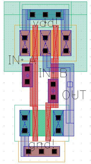
106 ]^`_ba>cdfebgihkjmlon>a(prqrstqruwvyxzpd { e
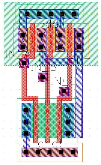
107 ]^`_ba>cd%h(g5}fjmlon>a(prqrstqruwvyxzpd { h
![].^`_baoc~d+}ogihki >x](/docs-images/72/66537718/images/108-0.jpg "d+qrƒbl( t bdvc ˆxznon>^ lo_mš")
108 ].^`_baoc~d+}ogihki >x d+qrƒbl( t bdvc ˆxznon>^ lo_mš ƒ( ŒS{ }
![].^ _ aoc~dž6gis](/docs-images/72/66537718/images/109-0.jpg "l>xb ƒ _M ao")
109 ].^ _ aoc~dž6gis l>xb ƒ _M ao 3dVcV{ Ž
![]^`_ba>cd% (g5](/docs-images/72/66537718/images/110-0.jpg "a( Sd cr t].")
110 ]^`_ba>cd% (g5 a( Sd cr t].] e {
![]^`_ba>cd+ og5](/docs-images/72/66537718/images/111-0.jpg "a( Sd cr t].")
111 ]^`_ba>cd+ og5 a( Sd cr t].] ho{
![]^`_ba>cd Zg5](/docs-images/72/66537718/images/112-0.jpg "a( Sd cr t].")
112 ]^`_ba>cd Zg5 a( Sd cr t].] }>{
![]^`_ba>cd+ og5](/docs-images/72/66537718/images/113-0.jpg "a( Sd cr t].")
113 ]^`_ba>cd+ og5 a( Sd cr t].] Ž6{
![].^ _ aocd+š>g4](/docs-images/72/66537718/images/114-0.jpg "a( Sd ct t]4] {")
114 ].^ _ aocd+š>g4 a( Sd ct t]4] { š
![].^`_baoc~dfev >giš ƒ œfœkƒ l( m d](/docs-images/72/66537718/images/115-0.jpg "lpp~cƒ ^` žš xzn>x ^ pƒbcsrcc x Ÿb{")
115 ].^`_baoc~dfev >giš ƒ œfœkƒ l( m d lpp~cƒ ^` žš xzn>x ^ pƒbcsrcc x Ÿb{ ev
![].^`_baoc~dfebe](/docs-images/72/66537718/images/116-0.jpg "giš xbcc~ÿj ^ p {")
116 ].^`_baoc~dfebe giš xbcc~ÿj ^ p { ebe
![].^`_baoc~dfe hogiš `ƒ(](/docs-images/72/66537718/images/117-0.jpg "Œbd Š ƒbœfn>xbc~xzpƒ cv{")
117 ].^`_baoc~dfe hogiš `ƒ( Œbd Š ƒbœfn>xbc~xzpƒ cv{ e h
![].^ _ aoc~dke }og"š](/docs-images/72/66537718/images/118-0.jpg "ƒbc~c~dv $p~^ ƒ l ;ƒb_b^ˆ")
118 ].^ _ aoc~dke }og"š ƒbc~c~dv $p~^ ƒ l ;ƒb_b^ˆ z{ ev}
![].^`_baoc~dfe Ž>g5 xb p Zp~xz_ d+ur^](/docs-images/72/66537718/images/119-0.jpg "3dVcdVlPp^ˆxz.")
119 ].^`_baoc~dfe Ž>g5 xb p Zp~xz_ d+ur^ 3dVcdVlPp^ˆxz.Š ƒ œkn6xzc x=pƒ cv{ e Ž
![].^`_baoc~dfe og4ut^ 3dVcdVl](/docs-images/72/66537718/images/120-0.jpg "p~^`xb.")
120 ].^`_baoc~dfe og4ut^ 3dVcdVl p~^`xb.š ƒbœfn>xbc~xzpƒ cv{ e
![].^ _ aocdfe og5](/docs-images/72/66537718/images/121-0.jpg "i d l Pp~xb_bdb{")
121 ].^ _ aocdfe og5 i d l Pp~xb_bdb{ ev
![].^`_baoc~dfe](/docs-images/72/66537718/images/122-0.jpg "Zg\" o Pp xz_")
122 ].^`_baoc~dfe Zg" o Pp xz_ db{ e
![].^`_baoc~dfev](/docs-images/72/66537718/images/123-0.jpg ">g5vyxb^ l6 p xz_bd")
123 ].^`_baoc~dfev >g5vyxb^ l6 p xz_bd { ev
![].^ _ aocdfe šog5 xb](/docs-images/72/66537718/images/124-0.jpg "^` jmlz bdvc p~d c {")
124 ].^ _ aocdfe šog5 xb ^` jmlz bdvc p~d c { evš
![].^ _ aocd%hb og5 ;x](/docs-images/72/66537718/images/125-0.jpg "pr Pp xz_bd+stuyšt{")
125 ].^ _ aocd%hb og5 ;x pr Pp xz_bd+stuyšt{ hz
![].^`_baoc~d%h(ebg5](/docs-images/72/66537718/images/126-0.jpg "xb p Zp~xz_ db{")
126 ].^`_baoc~d%h(ebg5 xb p Zp~xz_ db{ h(e
![]^`_ba>cd%hbhog" tn6dvc~xzp^`ƒbl>xb S c](/docs-images/72/66537718/images/127-0.jpg "xzl> ~ ƒ l> (a> p~xzl6 dys œfno `^ >dvcv{")
127 ]^`_ba>cd%hbhog" tn6dvc~xzp^`ƒbl>xb S c xzl> ~ ƒ l> (a> p~xzl6 dys œfno `^ >dvcv{ hbh
![].^ _ aoc~d+hb}og"](/docs-images/72/66537718/images/128-0.jpg "ta(p~noa(prutc^`")
128 ].^ _ aoc~d+hb}og" ta(p~noa(prutc^` bdvcv{ hz}
![].^ _ aocd%hzž>gi Z o^](/docs-images/72/66537718/images/129-0.jpg "ª«pt dv_b^ˆ p~d c {")
129 ].^ _ aocd%hzž>gi Z o^ ª«pt dv_b^ˆ p~d c { h=ž
![].^ _ aocd%h (gi](/docs-images/72/66537718/images/130-0.jpg "Zao ( mu sršt{")
130 ].^ _ aocd%h (gi Zao ( mu sršt{ hb
![]^`_ba>cd%hz](/docs-images/72/66537718/images/131-0.jpg ">g4 tq %{ hz")
131 ]^`_ba>cd%hz >g4 tq %{ hz
![].^ _](/docs-images/72/66537718/images/132-0.jpg "aoc~d+hp Zg4")
132 ].^ _ aoc~d+hp Zg4 t +{ h
![].^`_baoc~d%hz >g4].](/docs-images/72/66537718/images/133-0.jpg "^`l>xz 4Š o^ n x")
133 ].^`_baoc~d%hz >g4].^`l>xz 4Š o^ n x ŸbƒbaopV{ hz
An Analog Phase-Locked Loop
 1 An Analog Phase-Locked Loop Greg Flewelling ABSTRACT This report discusses the design, simulation, and layout of an Analog Phase-Locked Loop (APLL). The circuit consists of five major parts: A differential
Analog CMOS Interface Circuits for UMSI Chip of Environmental Monitoring Microsystem
 Analog CMOS Interface Circuits for UMSI Chip of Environmental Monitoring Microsystem A report Submitted to Canopus Systems Inc. Zuhail Sainudeen and Navid Yazdi Arizona State University July 2001 1. Overview
IMPLEMENTING THE 10-BIT, 50MS/SEC PIPELINED ADC
 98 CHAPTER 5 IMPLEMENTING THE 0-BIT, 50MS/SEC PIPELINED ADC 99 5.0 INTRODUCTION This chapter is devoted to describe the implementation of a 0-bit, 50MS/sec pipelined ADC with different stage resolutions
INTEGRATED CIRCUITS. AN109 Microprocessor-compatible DACs Dec
 INTEGRATED CIRCUITS 1988 Dec DAC products are designed to convert a digital code to an analog signal. Since a common source of digital signals is the data bus of a microprocessor, DAC circuits that are
CMOS High Speed A/D Converter Architectures
 CHAPTER 3 CMOS High Speed A/D Converter Architectures 3.1 Introduction In the previous chapter, basic key functions are examined with special emphasis on the power dissipation associated with its implementation.
UMAINE ECE Morse Code ROM and Transmitter at ISM Band Frequency
 UMAINE ECE Morse Code ROM and Transmitter at ISM Band Frequency Jamie E. Reinhold December 15, 2011 Abstract The design, simulation and layout of a UMAINE ECE Morse code Read Only Memory and transmitter
8-Bit, high-speed, µp-compatible A/D converter with track/hold function ADC0820
 8-Bit, high-speed, µp-compatible A/D converter with DESCRIPTION By using a half-flash conversion technique, the 8-bit CMOS A/D offers a 1.5µs conversion time while dissipating a maximum 75mW of power.
IN the design of the fine comparator for a CMOS two-step flash A/D converter, the main design issues are offset cancelation
 JOURNAL OF STELLAR EE315 CIRCUITS 1 A 60-MHz 150-µV Fully-Differential Comparator Erik P. Anderson and Jonathan S. Daniels (Invited Paper) Abstract The overall performance of two-step flash A/D converters
10-Bit µp-compatible D/A converter
 DESCRIPTION The is a microprocessor-compatible monolithic 10-bit digital-to-analog converter subsystem. This device offers 10-bit resolution and ±0.1% accuracy and monotonicity guaranteed over full operating
d. Can you find intrinsic gain more easily by examining the equation for current? Explain.
 EECS140 Final Spring 2017 Name SID 1. [8] In a vacuum tube, the plate (or anode) current is a function of the plate voltage (output) and the grid voltage (input). I P = k(v P + µv G ) 3/2 where µ is a
ECE 6770 FINAL PROJECT
 ECE 6770 FINAL PROJECT POINT TO POINT COMMUNICATION SYSTEM Submitted By: Omkar Iyer (Omkar_iyer82@yahoo.com) Vamsi K. Mudarapu (m_vamsi_krishna@yahoo.com) MOTIVATION Often in the real world we have situations
Advanced Operational Amplifiers
 IsLab Analog Integrated Circuit Design OPA2-47 Advanced Operational Amplifiers כ Kyungpook National University IsLab Analog Integrated Circuit Design OPA2-1 Advanced Current Mirrors and Opamps Two-stage
CONTINUOUS DIGITAL CALIBRATION OF PIPELINED A/D CONVERTERS
 CONTINUOUS DIGITAL CALIBRATION OF PIPELINED A/D CONVERTERS By Alma Delić-Ibukić B.S. University of Maine, 2002 A THESIS Submitted in Partial Fulfillment of the Requirements for the Degree of Master of
A 80Ms/sec 10bit PIPELINED ADC Using 1.5Bit Stages And Built-in Digital Error Correction Logic
 A 80Ms/sec 10bit PIPELINED ADC Using 1.5Bit Stages And Built-in Digital Error Correction Logic Abstract P.Prasad Rao 1 and Prof.K.Lal Kishore 2, 1 Research Scholar, JNTU-Hyderabad prasadrao_hod@yahoo.co.in
CHAPTER 6 PHASE LOCKED LOOP ARCHITECTURE FOR ADC
 138 CHAPTER 6 PHASE LOCKED LOOP ARCHITECTURE FOR ADC 6.1 INTRODUCTION The Clock generator is a circuit that produces the timing or the clock signal for the operation in sequential circuits. The circuit
Design of a Folded Cascode Operational Amplifier in a 1.2 Micron Silicon-Carbide CMOS Process
 University of Arkansas, Fayetteville ScholarWorks@UARK Electrical Engineering Undergraduate Honors Theses Electrical Engineering 5-2017 Design of a Folded Cascode Operational Amplifier in a 1.2 Micron
8-Bit A/D Converter AD673 REV. A FUNCTIONAL BLOCK DIAGRAM
 a FEATURES Complete 8-Bit A/D Converter with Reference, Clock and Comparator 30 s Maximum Conversion Time Full 8- or 16-Bit Microprocessor Bus Interface Unipolar and Bipolar Inputs No Missing Codes Over
Design of 1.8V, 72MS/s 12 Bit Pipeline ADC in 0.18µm Technology
 Design of 1.8V, 72MS/s 12 Bit Pipeline ADC in 0.18µm Technology Ravi Kumar 1, Seema Kanathe 2 ¹PG Scholar, Department of Electronics and Communication, Suresh GyanVihar University, Jaipur, India ²Assistant
Low Cost 10-Bit Monolithic D/A Converter AD561
 a FEATURES Complete Current Output Converter High Stability Buried Zener Reference Laser Trimmed to High Accuracy (1/4 LSB Max Error, AD561K, T) Trimmed Output Application Resistors for 0 V to +10 V, 5
Optimizing the Stage Resolution of a 10-Bit, 50 Ms/Sec Pipelined A/D Converter & Its Impact on Speed, Power, Area, and Linearity
 Circuits and Systems, 202, 3, 66-75 http://dx.doi.org/0.4236/cs.202.32022 Published Online April 202 (http://www.scirp.org/journal/cs) Optimizing the Stage Resolution of a 0-Bit, 50 Ms/Sec Pipelined A/D
Summary Last Lecture
 EE247 Lecture 23 Converters Techniques to reduce flash complexity Interpolating (continued) Folding Multi-Step s Two-Step flash Pipelined s EECS 247 Lecture 23: Data Converters 26 H.K. Page Summary Last
Chapter 3 Novel Digital-to-Analog Converter with Gamma Correction for On-Panel Data Driver
 Chapter 3 Novel Digital-to-Analog Converter with Gamma Correction for On-Panel Data Driver 3.1 INTRODUCTION As last chapter description, we know that there is a nonlinearity relationship between luminance
Summary Last Lecture
 EE247 Lecture 23 Converters Techniques to reduce flash complexity Interpolating (continued) Folding Multi-Step s Two-Step flash Pipelined s EECS 247 Lecture 23: Data Converters 26 H.K. Page 1 Summary Last
Operational Amplifier with Two-Stage Gain-Boost
 Proceedings of the 6th WSEAS International Conference on Simulation, Modelling and Optimization, Lisbon, Portugal, September 22-24, 2006 482 Operational Amplifier with Two-Stage Gain-Boost FRANZ SCHLÖGL
Hello, and welcome to the TI Precision Labs video series discussing comparator applications. The comparator s job is to compare two analog input
 Hello, and welcome to the TI Precision Labs video series discussing comparator applications. The comparator s job is to compare two analog input signals and produce a digital or logic level output based
A PSEUDO-CLASS-AB TELESCOPIC-CASCODE OPERATIONAL AMPLIFIER
 A PSEUDO-CLASS-AB TELESCOPIC-CASCODE OPERATIONAL AMPLIFIER M. Taherzadeh-Sani, R. Lotfi, and O. Shoaei ABSTRACT A novel class-ab architecture for single-stage operational amplifiers is presented. The structure
AD557 SPECIFICATIONS. T A = 25 C, V CC = 5 V unless otherwise noted) REV. B
 REV. B") SPECIFICATIONS Model Min Typ Max Unit RESOLUTION 8 Bits RELATIVE ACCURACY 0 C to 70 C ± 1/2 1 LSB Ranges 0 to 2.56 V Current Source 5 ma Sink Internal Passive Pull-Down to Ground 2 SETTLING TIME 3 0.8
SPECIFICATIONS Model Min Typ Max Unit RESOLUTION 8 Bits RELATIVE ACCURACY 0 C to 70 C ± 1/2 1 LSB Ranges 0 to 2.56 V Current Source 5 ma Sink Internal Passive Pull-Down to Ground 2 SETTLING TIME 3 0.8
CHAPTER 3 DESIGN OF PIPELINED ADC USING SCS-CDS AND OP-AMP SHARING TECHNIQUE
 CHAPTER 3 DESIGN OF PIPELINED ADC USING SCS-CDS AND OP-AMP SHARING TECHNIQUE 3.1 INTRODUCTION An ADC is a device which converts a continuous quantity into discrete digital signal. Among its types, pipelined
Design of Pipeline Analog to Digital Converter
 Design of Pipeline Analog to Digital Converter Vivek Tripathi, Chandrajit Debnath, Rakesh Malik STMicroelectronics The pipeline analog-to-digital converter (ADC) architecture is the most popular topology
Radivoje Đurić, 2015, Analogna Integrisana Kola 1
 OTA-output buffer 1 According to the types of loads, the driving capability of the output stages differs. For switched capacitor circuits which have high impedance capacitive loads, class A output stage
A 24 V Chopper Offset-Stabilized Operational Amplifier with Symmetrical RC Notch Filters having sub-10 µv offset and over-120db CMRR
 ROMANIAN JOURNAL OF INFORMATION SCIENCE AND TECHNOLOGY Volume 20, Number 4, 2017, 301 312 A 24 V Chopper Offset-Stabilized Operational Amplifier with Symmetrical RC Notch Filters having sub-10 µv offset
CMOS Operational Amplifier
 The George Washington University Department of Electrical and Computer Engineering Course: ECE218 Instructor: Mona E. Zaghloul Students: Shunping Wang Yiping (Neil) Tsai Data: 05/14/07 Introduction In
Design of High-Speed Op-Amps for Signal Processing
 Design of High-Speed Op-Amps for Signal Processing R. Jacob (Jake) Baker, PhD, PE Professor and Chair Boise State University 1910 University Dr. Boise, ID 83725-2075 jbaker@ieee.org Abstract - As CMOS
Index terms: Analog to Digital conversion, capacitor sharing, high speed OPAMP-sharing pipelined analog to digital convertor, Low power.
 Pipeline ADC using Switched Capacitor Sharing Technique with 2.5 V, 10-bit Ankit Jain Dept. of Electronics and Communication, Indore Institute of Science & Technology, Indore, India Abstract: This paper
Analog I/O. ECE 153B Sensor & Peripheral Interface Design Winter 2016
 Analog I/O ECE 153B Sensor & Peripheral Interface Design Introduction Anytime we need to monitor or control analog signals with a digital system, we require analogto-digital (ADC) and digital-to-analog
6-Bit A/D converter (parallel outputs)
") DESCRIPTION The is a low cost, complete successive-approximation analog-to-digital (A/D) converter, fabricated using Bipolar/I L technology. With an external reference voltage, the will accept input voltages
DESCRIPTION The is a low cost, complete successive-approximation analog-to-digital (A/D) converter, fabricated using Bipolar/I L technology. With an external reference voltage, the will accept input voltages
Tel: Fax:
 B Tel: 78.39.4700 Fax: 78.46.33 SPECIFICATIONS (T A = +5 C, V+ = +5 V, V = V or 5 V, all voltages measured with respect to digital common, unless otherwise noted) AD57J AD57K AD57S Model Min Typ Max Min
P a g e 1. Introduction
 P a g e 1 Introduction 1. Signals in digital form are more convenient than analog form for processing and control operation. 2. Real world signals originated from temperature, pressure, flow rate, force
DACPORT Low Cost, Complete P-Compatible 8-Bit DAC AD557*
 a FEATURES Complete 8-Bit DAC Voltage Output 0 V to 2.56 V Internal Precision Band-Gap Reference Single-Supply Operation: 5 V ( 10%) Full Microprocessor Interface Fast: 1 s Voltage Settling to 1/2 LSB
Electronic Circuits EE359A
 Electronic Circuits EE359A Bruce McNair B206 bmcnair@stevens.edu 201-216-5549 1 Memory and Advanced Digital Circuits - 2 Chapter 11 2 Figure 11.1 (a) Basic latch. (b) The latch with the feedback loop opened.
A 12-bit Interpolated Pipeline ADC using Body Voltage Controlled Amplifier
 A 12-bit Interpolated Pipeline ADC using Body Voltage Controlled Amplifier Hyunui Lee, Masaya Miyahara, and Akira Matsuzawa Tokyo Institute of Technology, Japan Outline Background Body voltage controlled
Design and Simulation of Low Voltage Operational Amplifier
 Design and Simulation of Low Voltage Operational Amplifier Zach Nelson Department of Electrical Engineering, University of Nevada, Las Vegas 4505 S Maryland Pkwy, Las Vegas, NV 89154 United States of America
A 4 GSample/s 8-bit ADC in. Ken Poulton, Robert Neff, Art Muto, Wei Liu, Andrew Burstein*, Mehrdad Heshami* Agilent Laboratories Palo Alto, California
 A 4 GSample/s 8-bit ADC in 0.35 µm CMOS Ken Poulton, Robert Neff, Art Muto, Wei Liu, Andrew Burstein*, Mehrdad Heshami* Agilent Laboratories Palo Alto, California 1 Outline Background Chip Architecture
Low-Power Pipelined ADC Design for Wireless LANs
 Low-Power Pipelined ADC Design for Wireless LANs J. Arias, D. Bisbal, J. San Pablo, L. Quintanilla, L. Enriquez, J. Vicente, J. Barbolla Dept. de Electricidad y Electrónica, E.T.S.I. de Telecomunicación,
NOVEMBER 28, 2016 COURSE PROJECT: CMOS SWITCHING POWER SUPPLY EE 421 DIGITAL ELECTRONICS ERIC MONAHAN
 NOVEMBER 28, 2016 COURSE PROJECT: CMOS SWITCHING POWER SUPPLY EE 421 DIGITAL ELECTRONICS ERIC MONAHAN 1.Introduction: CMOS Switching Power Supply The course design project for EE 421 Digital Engineering
CMOS ADC & DAC Principles
 CMOS ADC & DAC Principles Willy Sansen KULeuven, ESAT-MICAS Leuven, Belgium willy.sansen@esat.kuleuven.be Willy Sansen 10-05 201 Table of contents Definitions Digital-to-analog converters Resistive Capacitive
ECEN689: Special Topics in High-Speed Links Circuits and Systems Spring 2012
 ECEN689: Special Topics in High-Speed Links Circuits and Systems Spring 2012 Lecture 5: Termination, TX Driver, & Multiplexer Circuits Sam Palermo Analog & Mixed-Signal Center Texas A&M University Announcements
DESIGN AND PERFORMANCE VERIFICATION OF CURRENT CONVEYOR BASED PIPELINE A/D CONVERTER USING 180 NM TECHNOLOGY
 DESIGN AND PERFORMANCE VERIFICATION OF CURRENT CONVEYOR BASED PIPELINE A/D CONVERTER USING 180 NM TECHNOLOGY Neha Bakawale Departmentof Electronics & Instrumentation Engineering, Shri G. S. Institute of
UNIT-II LOW POWER VLSI DESIGN APPROACHES
 UNIT-II LOW POWER VLSI DESIGN APPROACHES Low power Design through Voltage Scaling: The switching power dissipation in CMOS digital integrated circuits is a strong function of the power supply voltage.
Chapter 5. Operational Amplifiers and Source Followers. 5.1 Operational Amplifier
 Chapter 5 Operational Amplifiers and Source Followers 5.1 Operational Amplifier In single ended operation the output is measured with respect to a fixed potential, usually ground, whereas in double-ended
ISSCC 2004 / SESSION 25 / HIGH-RESOLUTION NYQUIST ADCs / 25.4
 ISSCC 2004 / SESSION 25 / HIGH-RESOLUTION NYQUIST ADCs / 25.4 25.4 A 1.8V 14b 10MS/s Pipelined ADC in 0.18µm CMOS with 99dB SFDR Yun Chiu, Paul R. Gray, Borivoje Nikolic University of California, Berkeley,
444 Index. F Fermi potential, 146 FGMOS transistor, 20 23, 57, 83, 84, 98, 205, 208, 213, 215, 216, 241, 242, 251, 280, 311, 318, 332, 354, 407
 Index A Accuracy active resistor structures, 46, 323, 328, 329, 341, 344, 360 computational circuits, 171 differential amplifiers, 30, 31 exponential circuits, 285, 291, 292 multifunctional structures,
Quad 12-Bit Digital-to-Analog Converter (Serial Interface)
") Quad 1-Bit Digital-to-Analog Converter (Serial Interface) FEATURES COMPLETE QUAD DAC INCLUDES INTERNAL REFERENCES AND OUTPUT AMPLIFIERS GUARANTEED SPECIFICATIONS OVER TEMPERATURE GUARANTEED MONOTONIC OVER
Quad 1-Bit Digital-to-Analog Converter (Serial Interface) FEATURES COMPLETE QUAD DAC INCLUDES INTERNAL REFERENCES AND OUTPUT AMPLIFIERS GUARANTEED SPECIFICATIONS OVER TEMPERATURE GUARANTEED MONOTONIC OVER
Design of an Assembly Line Structure ADC
 Design of an Assembly Line Structure ADC Chen Hu 1, Feng Xie 1,Ming Yin 1 1 Department of Electronic Engineering, Naval University of Engineering, Wuhan, China Abstract This paper presents a circuit design
CMOS synchronous Buck switching power supply Raheel Sadiq November 28, 2016
 CMOS synchronous Buck switching power supply Raheel Sadiq November 28, 2016 Part 1: This part of the project is to lay out a bandgap. We previously built our bandgap in HW #13 which supplied a constant
Performance of Revised TVC Circuit. PSD8C Version 2.0. Dr. George L. Engel
 Performance of Revised TVC Circuit PSD8C Version 2. Dr. George L. Engel May, 21 I) Introduction This report attempts to document the performance of the revised TVC circuit. The redesign tried to correct
Designing of a 8-bits DAC in 0.35µm CMOS Technology For High Speed Communication Systems Application
 Designing of a 8-bits DAC in 035µm CMOS Technology For High Speed Communication Systems Application Veronica Ernita Kristianti, Hamzah Afandi, Eri Prasetyo ibowo, Brahmantyo Heruseto and shinta Kisriani
Tuesday, March 1st, 9:15 11:00. Snorre Aunet Nanoelectronics group Department of Informatics University of Oslo.
 Nyquist Analog to Digital it Converters Tuesday, March 1st, 9:15 11:00 Snorre Aunet (sa@ifi.uio.no) Nanoelectronics group Department of Informatics University of Oslo 3.1 Introduction 3.1.1 DAC applications
CMOS 12-Bit Multiplying DIGITAL-TO-ANALOG CONVERTER Microprocessor Compatible
 CMOS 12-Bit Multiplying DIGITAL-TO-ANALOG CONVERTER Microprocessor Compatible FEATURES FOUR-QUADRANT MULTIPLICATION LOW GAIN TC: 2ppm/ C typ MONOTONICITY GUARANTEED OVER TEMPERATURE SINGLE 5V TO 15V SUPPLY
ECEN 474/704 Lab 6: Differential Pairs
 ECEN 474/704 Lab 6: Differential Pairs Objective Design, simulate and layout various differential pairs used in different types of differential amplifiers such as operational transconductance amplifiers
Lecture 12 Memory Circuits. Memory Architecture: Decoders. Semiconductor Memory Classification. Array-Structured Memory Architecture RWM NVRWM ROM
 Semiconductor Memory Classification Lecture 12 Memory Circuits RWM NVRWM ROM Peter Cheung Department of Electrical & Electronic Engineering Imperial College London Reading: Weste Ch 8.3.1-8.3.2, Rabaey
A New, Low-Cost, Sampled-Data, 10-Bit CMOS A/D Converter
 A New, Low-Cost, Sampled-Data, 10-Bit CMOS A/D Converter IF IT S NOT LOW COST, IT S NOT CREATIVE Cost is the single most important factor in the success of any new product. The current emphasis on digital
Analysis and Design of High Speed Low Power Comparator in ADC
 Analysis and Design of High Speed Low Power Comparator in ADC 1 Abhishek Rai, 2 B Ananda Venkatesan 1 M.Tech Scholar, 2 Assistant professor Dept. of ECE, SRM University, Chennai 1 Abhishekfan1791@gmail.com,
Design of Analog and Mixed Integrated Circuits and Systems Theory Exercises
 102726 Design of nalog and Mixed Theory Exercises Francesc Serra Graells http://www.cnm.es/~pserra/uab/damics paco.serra@imb-cnm.csic.es 1 Introduction to the Design of nalog Integrated Circuits 1.1 The
A 10 bit, 1.8 GS/s Time Interleaved Pipeline ADC
 A 10 bit, 1.8 GS/s Time Interleaved Pipeline ADC M. Åberg 2, A. Rantala 2, V. Hakkarainen 1, M. Aho 1, J. Riikonen 1, D. Gomes Martin 2, K. Halonen 1 1 Electronic Circuit Design Laboratory Helsinki University
High Voltage and Temperature Auto Zero Op-Amp Cell Features Applications Process Technology Introduction Parameter Unit Rating
 Analogue Integration AISC11 High Voltage and Temperature Auto Zero Op-Amp Cell Rev.1 12-1-5 Features High Voltage Operation: 4.5-3 V Precision, Auto-Zeroed Input Vos High Temperature Operation Low Quiescent
ECE 415/515 ANALOG INTEGRATED CIRCUIT DESIGN
 ECE 415/515 ANALOG INTEGRATED CIRCUIT DESIGN OPAMP DESIGN AND SIMULATION Vishal Saxena OPAMP DESIGN PROJECT R 2 v out v in /2 R 1 C L v in v out V CM R L V CM C L V CM -v in /2 R 1 C L (a) (b) R 2 ECE415/EO
Rail to Rail Input Amplifier with constant G M and High Unity Gain Frequency. Arun Ramamurthy, Amit M. Jain, Anuj Gupta
 1 Rail to Rail Input Amplifier with constant G M and High Frequency Arun Ramamurthy, Amit M. Jain, Anuj Gupta Abstract A rail to rail input, 2.5V CMOS input amplifier is designed that amplifies uniformly
ECEN 474/704 Lab 5: Frequency Response of Inverting Amplifiers
 ECEN 474/704 Lab 5: Frequency Response of Inverting Amplifiers Objective Design, simulate and layout various inverting amplifiers. Introduction Inverting amplifiers are fundamental building blocks of electronic
EE584 Introduction to VLSI Design Final Project Document Group 9 Ring Oscillator with Frequency selector
 EE584 Introduction to VLSI Design Final Project Document Group 9 Ring Oscillator with Frequency selector Group Members Uttam Kumar Boda Rajesh Tenukuntla Mohammad M Iftakhar Srikanth Yanamanagandla 1 Table
CONVERTING 1524 SWITCHING POWER SUPPLY DESIGNS TO THE SG1524B
 LINEAR INTEGRATED CIRCUITS PS-5 CONVERTING 1524 SWITCHING POWER SUPPLY DESIGNS TO THE SG1524B Stan Dendinger Manager, Advanced Product Development Silicon General, Inc. INTRODUCTION Many power control
1. Short answer questions. (30) a. What impact does increasing the length of a transistor have on power and delay? Why? (6)
 a. What impact does increasing the length of a transistor have on power and delay? Why? (6)") CSE 493/593 Test 2 Fall 2011 Solution 1. Short answer questions. (30) a. What impact does increasing the length of a transistor have on power and delay? Why? (6) Decreasing of W to make the gate slower,
CSE 493/593 Test 2 Fall 2011 Solution 1. Short answer questions. (30) a. What impact does increasing the length of a transistor have on power and delay? Why? (6) Decreasing of W to make the gate slower,
Lecture 3 Switched-Capacitor Circuits Trevor Caldwell
 Advanced Analog Circuits Lecture 3 Switched-Capacitor Circuits Trevor Caldwell trevor.caldwell@analog.com Lecture Plan Date Lecture (Wednesday 2-4pm) Reference Homework 2017-01-11 1 MOD1 & MOD2 ST 2, 3,
Octal Sample-and-Hold with Multiplexed Input SMP18
 a FEATURES High Speed Version of SMP Internal Hold Capacitors Low Droop Rate TTL/CMOS Compatible Logic Inputs Single or Dual Supply Operation Break-Before-Make Channel Addressing Compatible With CD Pinout
High Precision 10 V IC Reference AD581
 High Precision 0 V IC Reference FEATURES Laser trimmed to high accuracy 0.000 V ±5 mv (L and U models) Trimmed temperature coefficient 5 ppm/ C maximum, 0 C to 70 C (L model) 0 ppm/ C maximum, 55 C to
Eliminate Pipeline Headaches with New 12-Bit 3Msps SAR ADC by Dave Thomas and William C. Rempfer
 A new 12-bit 3Msps ADC brings new levels of performance and ease of use to high speed ADC applications. By raising the speed of the successive approximation (SAR) method to 3Msps, it eliminates the many
Lecture 240 Cascode Op Amps (3/28/10) Page 240-1
 Page 240-1") Lecture 240 Cascode Op Amps (3/28/10) Page 2401 LECTURE 240 CASCODE OP AMPS LECTURE ORGANIZATION Outline Lecture Organization Single Stage Cascode Op Amps Two Stage Cascode Op Amps Summary CMOS Analog
Lecture 240 Cascode Op Amps (3/28/10) Page 2401 LECTURE 240 CASCODE OP AMPS LECTURE ORGANIZATION Outline Lecture Organization Single Stage Cascode Op Amps Two Stage Cascode Op Amps Summary CMOS Analog
EE 330 Lecture 42. Other Logic Styles Digital Building Blocks
 EE 330 Lecture 42 Other Logic Styles Digital Building Blocks Logic Styles Static CMOS Complex Logic Gates Pass Transistor Logic (PTL) Pseudo NMOS Dynamic Logic Domino Zipper Static CMOS Widely used Attractive
An Improved Recycling Folded Cascode OTA with positive feedback
 An Improved Recycling Folded Cascode OTA with positive feedback S.KUMARAVEL, B.VENKATARAMANI Department of Electronics and Communication Engineering National Institute of Technology Trichy Tiruchirappalli
Topic 6. CMOS Static & Dynamic Logic Gates. Static CMOS Circuit. NMOS Transistors in Series/Parallel Connection
 NMOS Transistors in Series/Parallel Connection Topic 6 CMOS Static & Dynamic Logic Gates Peter Cheung Department of Electrical & Electronic Engineering Imperial College London Transistors can be thought
DESIGN OF A FULLY DIFFERENTIAL HIGH-SPEED HIGH-PRECISION AMPLIFIER
 DESIGN OF A FULLY DIFFERENTIAL HIGH-SPEED HIGH-PRECISION AMPLIFIER Mayank Gupta mayank@ee.ucla.edu N. V. Girish envy@ee.ucla.edu Design I. Design II. University of California, Los Angeles EE215A Term Project
An 11 Bit Sub- Ranging SAR ADC with Input Signal Range of Twice Supply Voltage
 D. Aksin, M.A. Al- Shyoukh, F. Maloberti: "An 11 Bit Sub-Ranging SAR ADC with Input Signal Range of Twice Supply Voltage"; IEEE International Symposium on Circuits and Systems, ISCAS 2007, New Orleans,
Enhancing the Slew rate and Gain Bandwidth of Single ended CMOS Operational Transconductance Amplifier using LCMFB Technique
 ISSN: 2278 1323 Enhancing the Slew rate and Gain Bandwidth of Single ended CMOS Operational Transconductance Amplifier using LCMFB Technique 1 Abhishek Singh, 2 Sunil Kumar Shah, 3 Pankaj Sahu 1 abhi16.2007@gmail.com,
CMOS Digital Integrated Circuits Lec 11 Sequential CMOS Logic Circuits
 Lec Sequential CMOS Logic Circuits Sequential Logic In Combinational Logic circuit Out Memory Sequential The output is determined by Current inputs Previous inputs Output = f(in, Previous In) The regenerative
EE 330 Lecture 43. Digital Circuits. Other Logic Styles Dynamic Logic Circuits
 EE 330 Lecture 43 Digital Circuits Other Logic Styles Dynamic Logic Circuits Review from Last Time Elmore Delay Calculations W M 5 V OUT x 20C RE V IN 0 L R L 1 L R RW 6 W 1 C C 3 D R t 1 R R t 2 R R t
CPE/EE 427, CPE 527 VLSI Design I: Homeworks 3 & 4
 CPE/EE 427, CPE 527 VLSI Design I: Homeworks 3 & 4 1 2 3 4 5 6 7 8 9 10 Sum 30 10 25 10 30 40 10 15 15 15 200 1. (30 points) Misc, Short questions (a) (2 points) Postponing the introduction of signals
A 2.4 GHZ RECEIVER IN SILICON-ON-SAPPHIRE MICHAEL PETERS. B.S., Kansas State University, 2009 A REPORT
 A 2.4 GHZ RECEIVER IN SILICON-ON-SAPPHIRE by MICHAEL PETERS B.S., Kansas State University, 2009 A REPORT submitted in partial fulfillment of the requirements for the degree MASTER OF SCIENCE Department
Modeling and Implementation of A 6-Bit, 50MHz Pipelined ADC in CMOS
 Master s Thesis Modeling and Implementation of A 6-Bit, 50MHz Pipelined ADC in CMOS Qazi Omar Farooq Department of Electrical and Information Technology, Faculty of Engineering, LTH, Lund University, 2016.
A 35 fj 10b 160 MS/s Pipelined- SAR ADC with Decoupled Flip- Around MDAC and Self- Embedded Offset Cancellation
 Y. Zu, C.- H. Chan, S.- W. Sin, S.- P. U, R.P. Martins, F. Maloberti: "A 35 fj 10b 160 MS/s Pipelined-SAR ADC with Decoupled Flip-Around MDAC and Self- Embedded Offset Cancellation"; IEEE Asian Solid-
Implementing a 5-bit Folding and Interpolating Analog to Digital Converter
 Implementing a 5-bit Folding and Interpolating Analog to Digital Converter Zachary A Pfeffer (pfefferz@colorado.edu) Department of Electrical and Computer Engineering University of Colorado, Boulder CO
EE 330 Lecture 43. Digital Circuits. Other Logic Styles Dynamic Logic Circuits
 EE 330 Lecture 43 Digital Circuits Other Logic Styles Dynamic Logic Circuits Review from Last Time Elmore Delay Calculations W M 5 V OUT x 20C RE V IN 0 L R L 1 L R R 6 W 1 C C 3 D R t 1 R R t 2 R R t
Design of Low Power High Speed Fully Dynamic CMOS Latched Comparator
 International Journal of Engineering Research and Development e-issn: 2278-067X, p-issn: 2278-800X, www.ijerd.com Volume 10, Issue 4 (April 2014), PP.01-06 Design of Low Power High Speed Fully Dynamic
LM125 Precision Dual Tracking Regulator
 LM125 Precision Dual Tracking Regulator INTRODUCTION The LM125 is a precision, dual, tracking, monolithic voltage regulator. It provides separate positive and negative regulated outputs, thus simplifying
INF4420 Switched capacitor circuits Outline
 INF4420 Switched capacitor circuits Spring 2012 1 / 54 Outline Switched capacitor introduction MOSFET as an analog switch z-transform Switched capacitor integrators 2 / 54 Introduction Discrete time analog
Chapter 13: Introduction to Switched- Capacitor Circuits
 Chapter 13: Introduction to Switched- Capacitor Circuits 13.1 General Considerations 13.2 Sampling Switches 13.3 Switched-Capacitor Amplifiers 13.4 Switched-Capacitor Integrator 13.5 Switched-Capacitor
9-Bit, 30 MSPS ADC AD9049 REV. 0. Figure 1. Typical Connections FUNCTIONAL BLOCK DIAGRAM
 a FEATURES Low Power: 00 mw On-Chip T/H, Reference Single +5 V Power Supply Operation Selectable 5 V or V Logic I/O Wide Dynamic Performance APPLICATIONS Digital Communications Professional Video Medical
Microprocessor-Compatible 12-Bit D/A Converter AD667*
 a FEATURES Complete 12-Bit D/A Function Double-Buffered Latch On Chip Output Amplifier High Stability Buried Zener Reference Single Chip Construction Monotonicity Guaranteed Over Temperature Linearity
Rail-To-Rail Output Op-Amp Design with Negative Miller Capacitance Compensation
 Rail-To-Rail Op-Amp Design with Negative Miller Capacitance Compensation Muhaned Zaidi, Ian Grout, Abu Khari bin A ain Abstract In this paper, a two-stage op-amp design is considered using both Miller
320MHz Digital Phase Lock Loop. Patrick Spinney Department of Electrical Engineering University of Maine
 320MHz Digital Phase Lock Loop Patrick Spinney Department of Electrical Engineering University of Maine December 2004 Abstract DPLLs (Digital Phase Locked Loop) are commonly used in communications systems.
Design and Layout of Two Stage High Bandwidth Operational Amplifier
 Design and Layout of Two Stage High Bandwidth Operational Amplifier Yasir Mahmood Qureshi Abstract This paper presents the design and layout of a two stage, high speed operational amplifiers using standard