InAlN/GaN HEMTs Technologies for Microwave, Fast switching and Mixed Signal Applications
|
|
|
- Kristina Cox
- 5 years ago
- Views:
Transcription


1 InAlN/GaN HEMTs Technologies for Microwave, Fast switching and Mixed Signal Applications S.DELAGE / S.PIOTROWICZ
2 Summary III-V Lab presentation Motivations Technology for L & S band applications Technology for X to Ka band applications Fast Switching applications E/D mode devices for mixed signal applications Page 2
3 III-V Lab presentation V18 What is III-V Lab? A jointly owned Alcatel-Lucent / Thales /CEA R&D Lab French GIE (Groupement d Intérêt Economique) organization with about 150 R&D experts (incl. 25 from CEA-Leti + ~18 PhD students) Dedicated to epitaxial growth, device and circuit design and manufacturing performing R&T on III-V semiconductor technology and integration with Si circuits and micro-systems Optoelectronic and microelectronic materials, devices and circuits From basic research to technology transfer for industrialisation or to small scale and pilot line production for complementary Alcatel-Lucent / Thales applications High bit rate Optical Fibre and Wireless Telecommunications Microwave and Photonic systems for Defence, Security and Space and looking for valorisation through external cooperation December 2012 Page 3 Page 3
 ~ 50p. 40% Alcatel Lucent Bell Labs Fr. ~ 50p. 40% CEA Leti 20% R&D contracts 22~35 p/y Leti technology platforms December 2012 Page 4 Page 4")
4 III-V Lab presentation V18 CEA-Leti : third partner in III-V Lab Alcatel-Thales III-V Lab becomes III-V Lab Access to Leti Si microelectronic and microsystem technology platforms Thales (TRT Fr) ~ 50p. 40% Alcatel Lucent Bell Labs Fr. ~ 50p. 40% CEA Leti 20% R&D contracts 22~35 p/y Leti technology platforms December 2012 Page 4 Page 4
5 III-V Lab presentation V18 Main research activities and applications Opto-electronics Tx/Rx photonic integrated circuits for the next generations of opticalfibre communication networks : 10x10Gb/s, 40Gb/s and above, 100Gb/s Ethernet IR laser diodes and photonic micro-systems for optronic systems : DIRCM, detection of toxic gases and explosives, microwave links over optical fibres, laser pumping for atomic clocks and cold atoms sensors Advanced IR photo-detectors Micro-electronics GaN power HEMT MMIC technology for radars, electronic warfare, and wireless communication systems InP HBT technology for fast digital and mixed signal circuits : 40Gb/s and above front-end circuits, broadband ADCs, December 2012 Page 5 Page 5


6 III-V Lab presentation V18 III-V Lab implantation Thales Research and Technology Palaiseau Alcatel-Lucent /Bell Labs Fr. Marcoussis December 2012 Page 6 Page 6

7 7 Motivations : Why AlInN/GaN HEMTs? In 17 Al 83 N/GaN : - Spontaneous polarization without lattice mismatch Spontaneous polarization of GaN, InN and AlN compounds functions of lattice constant Spontaneous polarization higher : More electrons density More power density Lattice match : Less lag effects? Better reliability? ΔP 0 (Cm -2 ) Piezo (Cm -2 ) Ns (cm -2 ) Al 30 Ga 70 N/GaN In 17 Al 83 N/GaN Page 7


8 Structure of InAlN HEMTs Source : EPFL-UltraGaN Project Structure of studied 5nm -> 50% of the 11nm -> 85% of the charges AlN layer enhances sheet carrier mobility Sheet resistance # 320 W/sq. Sheet carrier density ns # 1.5E 13 cm -2 Page 8
9 Technology for S-Band Applications Technology for S-Band Applications Page 9

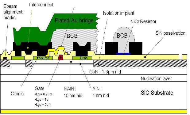
10 Power Device Manufacturing 2 inch Device cross section Page 10
11 Ig,Id (ma/mm) Id (ma/mm) Gm (ms/mm) Static results Id Vgs (V) Ig Vgs (V) Gm Id Idss = 600mA/mm Ids max = Vds=+1V Gm max = Vgs=-0.6V Ig < 20 Vds=10V Page 11


12 Small Signal Characterization F T = 15 GHz F MAG =38 GHz Gm # 300 ms/mm Gd # 3.2 ms/mm 19 db of 2 GHz Cgs # 3.4 pf/mm Cgd # pf/mm Cds # pf/mm Page 12
13 Pout (dbm), PAE (%) & Gp (db) PAE (%) Large Signal Characterization On wafer large signal characterization : 2mm GHz Pout Pin (dbm) PAE Gp Pout = 39dBm (8W - 4W/mm) with PAE = 62% and Gp=10.7dB (Vds0=20V Ids0=60mA - Zl=17+j18 W) V 25V Pout (W/mm) 30V 35V Pout from 4 to 8W/mm with associated PAE from 62% to 53% (no re-tune at each vds) Page 13


14 Amplifier realization power package GaN die RF out RF in High K matching networks diamond Heat spreader InAlN/GaN based Power amplifier Can be measured in single ended or balanced configuration Page 14
15 Output power (W) and PAE (%) Gain (db) Output power (W) and PAE (%) Gain (db) L-Band (2GHz) High Power Packaged Amplifiers Measurements pulsed 10µs/10%. Pout CW mode. Pout Gp Gp PAE PAE Input power (W) Input power (W) Vds=30V and Ids 0 =0.1A Vds=30V and Ids 0 =0.1A. 105W - CW reached (Pdiss = 4.5W/mm -> Tchannel = 260 C ) 140W - pulsed conditions ( Tchannel = 125 C) Page 15
 First time a transistor operates up to 1000 C!")
16 High Temperature DC Measurements (ULM university Germany) First time a transistor operates up to 1000 C! Page 16
 0,5 0,4 0,3 0,2 0,1 0,0 0 2 4 6 8 10 at RT after 1000 C V DS (V) +2 V +1 V 0 V -1 V 10 0 10-1 10-2 10-3 10-4 10-5 10-6 10-7 10-8 1000 C 0,5 0,4 0,3")
17 I GS (ma/mm) I D (A/mm) Thermal stability of 3 nm barrier InAlN/GaN HEMTs 0,6 3.5 nm InAlN device at RT 0,6 3.5 nm InAlN device after 1000 C stress I D (A/mm) 0,5 0,4 0,3 0,2 0,1 0, at RT after 1000 C V DS (V) +2 V +1 V 0 V -1 V C 0,5 0,4 0,3 0,2 0,1 0, V DS (V) +2 V +1 V Ultra thin barrier (few nm) InAlN/GaN heterostructure still working after 1000 C for 30min step. Very promising for high robustness demanding applications. 0 V -1 V Gate voltage (V) Page 17
18 Technology for X to K-Band Applications Technology for X to Ka-Band Applications Page 18
 H 21 ² 0.25µm F T # 30 GHz F MAX # 80 GHz Vgs = -4.5 V (-4.5;25) 0.8 MSG/MAG Fk # 27 GHz 0.6 Vgs = 0.5 V 0.4 Vgs = -0.5 V Vgs = -1.5 V 14dB/10 GHz 0.2 Vgs = -2.5 V Vgs = -3.5 V 11.")
19 Id (A/mm) db 0.25µm technology - pulsed I-V and Sij results Idss ~ 1.2A/mm and Vgs = 0.5V Gm max ~ 450mS/mm Vp~ 3.8V Polarisation (Vgs0,Vds0) Vgs = -4.5 V (0;0) Vgs = -4.5 V (-4.5;0) H 21 ² 0.25µm F T # 30 GHz F MAX # 80 GHz Vgs = -4.5 V (-4.5;25) 0.8 MSG/MAG Fk # 27 GHz 0.6 Vgs = 0.5 V 0.4 Vgs = -0.5 V Vgs = -1.5 V 14dB/10 GHz 0.2 Vgs = -2.5 V Vgs = -3.5 V 11.5dB/20 GHz 0 Vgs = -4.5 V dB/30 GHz Vds (V) Pulsed I-V measurements Frequency (GHz) Page 19
20 Pout (W) PAE (%), & Gp (db) Load-Pull 10 GHz 250µs pulsed W (10.8W/mm) 5.7W (8.7W/mm) % 45% 40% 2 1 4W (6.6W/mm) Pin (dbm) Pin (dbm) 8x75µm - A-Class (500mA/mm) Vgs 0 =-2.1V Vds from 20V to 30V Output power from 6.6W/mm to 10.8W/mm PAE from 45% to 40% Page 20
 25 20 15 10")

21 Gain (db), Pout (dbm) PAE (%) World first demonstration of 20 GHz CW InAlN/GaN Power amplifier Vds 1st_stage =18V, Vds 2nd_stage =20V, Ids= 250mA/mm, Pin (dbm) Pout meas (dbm) 5 Pout mod (dbm) Gain meas (db) 0 Gain mod (db) PAE meas (%) PAE mod (%) 20GHz : Pout = 4.5W with 20% PAE and 12B of linear gain 20 GHz AlInN/GaN amplifier In test JIG Good comparison with the simulation Page 21
22 Technology for Fast Switching Applications Technology for Fast Switching Applications Page 22
23 Technology for Fast Switching Applications Enveloppe Tracking Puissance Alimentation DC Enveloppe (BP:5MHz): - Signaux I & Q - Signal enveloppe Traitement Modulateur de polarisation Puissance de Polarisation: 50V 5A Signal RF modulé Amplificateur Page 23


24 Cellule de commutation Mesures à Vdd=50V, fcommut=50 & 100MHz Mesures: Rch=500 Ohms, Vdd= 50V, DC = 50% 10ns Fcommut= 50 MHz 5ns Fcommut=100MHz Page 24

 Fenv=8MHz")
25 Modulateur à 4 niveaux Mesures d un signal sinusoïdal fcommutation=6*fenveloppe Fenv=3MHz (Fc=18MHz) Fenv=8MHz (Fc=48MHz) Page 25
26 Technology for Mixed-Signal Applications Technology for Mixed-Signal Applications Page 26

27 Technology for Mixed-Signal Applications TRIQUINT & University of Notre-Dame Page 27

28 Technology for Mixed-Signal Applications TRIQUINT & University of Notre-Dame Page 28
29 Remerciements Merci de votre attention! Contacts: Page 29
Partnering along the chain of innovation : III-V lab example
 Partnering along the chain of innovation : III-V lab example Dominique Pons Symposium Global Open Innovation Networks What is III-V Lab? a jointly owned Alcatel-Lucent / Thales R&D Lab French GIE (Groupement
Composants HEMT InAlGaN/GaN pour applications en bandes Ka et Q.
 Composants HEMT InAlGaN/GaN pour applications en bandes Ka et Q. Stéphane PIOTROWICZ, Olivier PATARD, Jean-Claude JACQUET, Piero GAMARRA, Christian DUA & Sylvain DELAGE RF & Microwave 22 mars 2018 Copyright
100nm GaN on Si: A Pioneering Technology to Enable High RF Power in Millimeter Wave Bands NEW ENGLAND IMAPS SYMPOSIUM MAY 5, 2015
 Innovating with III-V s 100nm GaN on Si: A Pioneering Technology to Enable High RF Power in Millimeter Wave Bands NEW ENGLAND IMAPS SYMPOSIUM MAY 5, 2015 By Dr Fabien ROBERT Sales & Application Team Manager,
GaN Technology for Microwave Applications in Ka and Q bands. S. Delage CAPABILITIES AND APPLICATIONS OF GaN DEVICES Microwave and RF 2015
 GaN Technology for Microwave Applications in Ka and Q bands S. Delage CAPABILITIES AND APPLICATIONS OF GaN DEVICES Microwave and RF 2015 R. Aubry, S. Bernard, M. Magis N. Michel, O. Patard, O. Drisse,
Microwave & RF 22 nd of March 2018 D. FLORIOT
 Microwave & RF 22 nd of March 2018 D. FLORIOT Outine Introduction GaN technology roadmap GH15-10 : Up to Ka band GH10 : Towards high frequency (Q / V bands) GaN : Technology & Integration 2 UMS at a glance
MECXQMM-60W. 8.3 to 10.3 GHz GaN HEMT Power Amplifier
 Pout (dbm), PAE(%) Functional Block Diagram Main Features 0.25µm GaN HEMT Technology 8.3 10.3 GHz full performances Frequency Range 60W Output Power @ Pin 40.5 dbm PAE > 33% @ Pin 40.5 dbm Linear Gain
GaN MMIC PAs for MMW Applicaitons
 GaN MMIC PAs for MMW Applicaitons Miroslav Micovic HRL Laboratories LLC, 311 Malibu Canyon Road, Malibu, CA 9265, U. S. A. mmicovic@hrl.com Motivation for High Frequency Power sources 6 GHz 11 GHz Frequency
MMA GHz 1W Traveling Wave Amplifier Data Sheet
 Features: Frequency Range:.1 2 GHz P3dB: +29 dbm Gain: 12.5 db Vdd =12 V Ids =5 ma Input and Output Fully Matched to 5 Ω Applications: Fiber optics communication systems Microwave and wireless communication
TGF Watt Discrete Power GaN on SiC HEMT. Key Features. Measured Performance. Primary Applications Space Military Broadband Wireless
 12 Watt Discrete Power GaN on SiC HEMT Key Features Frequency Range: DC - 18 GHz > 41 dbm Nominal Psat 55% Maximum PAE 15 db Nominal Power Gain Bias: Vd = 28-40 V, Idq = 250 ma, Vg = -3 V Typical Technology:
TGF Watt Discrete Power GaN on SiC HEMT. Key Features. Measured Performance. Primary Applications Space Military Broadband Wireless
 6 Watt Discrete Power GaN on SiC HEMT Key Features Frequency Range: DC - 18 GHz > 38 dbm Nominal Psat 55% Maximum PAE 15 db Nominal Power Gain Bias: Vd = 28-40 V, Idq = 125 ma, Vg = -3 V Typical Technology:
Gallium Nitride MMIC Power Amplifier
 Gallium Nitride MMIC Power Amplifier August 2015 Rev 4 DESCRIPTION AMCOM s is an ultra-broadband GaN MMIC power amplifier. It has 21dB gain, and >41dBm output power over the 0.03 to 6GHz band. This MMIC
TGF Watt Discrete Power GaN on SiC HEMT. Key Features. Primary Applications Defense & Aerospace Broadband Wireless. Product Description
 50 Watt Discrete Power GaN on SiC HEMT Key Features Frequency Range: DC - 18 GHz 47 dbm Nominal Psat 55% Maximum PAE 8.7 db Nominal Power Gain Bias: Vd = 28-35 V, Idq = 1 A, Vg = -3.6 V Typical Technology:
MECGaNC30. 4 to 6 GHz GaN HEMT Power Amplifier. Main Features. Product Description. Applications
 Main Features 0.25µm GaN HEMT Technology 4.1 5.9 GHz full performances Frequency Range W Output Power @ Pin 27.5 dbm 37% PAE @ Pin 27.5 dbm % PAE @ Pout Watt 27 db Small Signal Gain Product Description
= 25 C) Parameter 2.7 GHz 2.9 GHz 3.1 GHz 3.3 GHz 3.5 GHz Units Small Signal Gain db
 Parameter 2.7 GHz 2.9 GHz 3.1 GHz 3.3 GHz 3.5 GHz Units Small Signal Gain db") CMPA273575D 75 W, 2.7-3.5 GHz, GaN MMIC, Power Amplifier Cree s CMPA273575D is a gallium nitride (GaN) High Electron Mobility Transistor (HEMT) based monolithic microwave integrated circuit (MMIC). GaN
CMPA273575D 75 W, 2.7-3.5 GHz, GaN MMIC, Power Amplifier Cree s CMPA273575D is a gallium nitride (GaN) High Electron Mobility Transistor (HEMT) based monolithic microwave integrated circuit (MMIC). GaN
85W Power Transistor. GaN HEMT on SiC
 GaN HEMT on SiC Description The is a 85W Gallium Nitride High Electron Mobility Transistor. This product offers a general purpose and broadband solution for a variety of RF power applications such as radar
MMA M4. Features:
 Features: Frequency Range: 0.1 26.5 GHz P3dB: +27 dbm Gain: 12.5 db Vdd =8 to 12 V Ids =250 to 500 ma Input and Output Fully Matched to 50 Ω Surface Mount, RoHs Compliant QFN 4x4mm package Applications:
ARFTG Workshop, Boulder, December 2014
 ARFTG Workshop, Boulder, December 2014 Design and measurements of high-efficiency PAs with high PAR signals Zoya Popovic, Tibault Reveyrand, David Sardin, Mike Litchfield, Scott Schafer, Andrew Zai Department
= 25 C) Parameter 1.0 GHz 2.0 GHz 3.0 GHz 4.0 GHz 5.0 GHz 6.0 GHz Units. Gain db. 32 dbm W
 Parameter 1.0 GHz 2.0 GHz 3.0 GHz 4.0 GHz 5.0 GHz 6.0 GHz Units. Gain db. 32 dbm W") CMPA006005D 5 W, 0 MHz - 6.0 GHz, GaN MMIC, Power Amplifier Cree s CMPA006005D is a gallium nitride (GaN) High Electron Mobility Transistor (HEMT) based monolithic microwave integrated circuit (MMIC).
CMPA006005D 5 W, 0 MHz - 6.0 GHz, GaN MMIC, Power Amplifier Cree s CMPA006005D is a gallium nitride (GaN) High Electron Mobility Transistor (HEMT) based monolithic microwave integrated circuit (MMIC).
D1H010DA1 10 W, 6 GHz, GaN HEMT Die
 D1H010DA1 10 W, 6 GHz, GaN HEMT Die D1H010DA1 by Dynax is a Gallium Nitride (GaN) high electron mobility transistor (HEMT). The D1H010DA1, operating at 48 V, offers high efficiency, great gain, easy of
= 25 C) Parameter 8.0 GHz 9.0 GHz 10.0 GHz 11.0 GHz Units Small Signal Gain db P OUT. = 25 dbm W Power P IN
 Parameter 8.0 GHz 9.0 GHz 10.0 GHz 11.0 GHz Units Small Signal Gain db P OUT. = 25 dbm W Power P IN") CMPA80B05D 5 W, 8.0 -.0 GHz, GaN MMIC, Power Amplifier Cree s CMP80B05D is a gallium nitride (GaN) High Electron Mobility Transistor (HEMT) based monolithic microwave integrated circuit (MMIC). GaN has
CMPA80B05D 5 W, 8.0 -.0 GHz, GaN MMIC, Power Amplifier Cree s CMP80B05D is a gallium nitride (GaN) High Electron Mobility Transistor (HEMT) based monolithic microwave integrated circuit (MMIC). GaN has
III-Nitride microwave switches Grigory Simin
 Microwave Microelectronics Laboratory Department of Electrical Engineering, USC Research Focus: - Wide Bandgap Microwave Power Devices and Integrated Circuits - Physics, Simulation, Design and Characterization
Novel III-Nitride HEMTs
 IEEE EDS Distinguished Lecture Boston Chapter, July 6 2005 Novel III-Nitride HEMTs Professor Kei May Lau Department of Electrical and Electronic Engineering Hong Kong University of Science and Technology
Pulse IV and pulsed S-parameter Parametric Analysis with AMCAD PIV & AGILENT PNA-X
 Pulse IV and pulsed S-parameter Parametric Analysis with AMCAD PIV & AGILENT PNA-X Tony Gasseling gasseling@amcad-engineering.com 1 Components PA Design Flow Measurement system Measurement Data base Circuits
PRELIMINARY = 25 C) Parameter GHz 14.0 GHz 14.5 GHz Units Small Signal Gain db P SAT. = 26 dbm W P 3dB
 Parameter GHz 14.0 GHz 14.5 GHz Units Small Signal Gain db P SAT. = 26 dbm W P 3dB") CMPADE030D PRELIMINARY 30 W, 3.75-4.5 GHz, 40 V, GaN MMIC, Power Amplifier Cree s CMPADE030D is a gallium nitride (GaN) High Electron Mobility Transistor (HEMT) based monolithic microwave integrated circuit
CMPADE030D PRELIMINARY 30 W, 3.75-4.5 GHz, 40 V, GaN MMIC, Power Amplifier Cree s CMPADE030D is a gallium nitride (GaN) High Electron Mobility Transistor (HEMT) based monolithic microwave integrated circuit
AlGaN Polarization Graded Field Effect Transistors for High Linearity Microwave Applications
 AlGaN Polarization Graded Field Effect Transistors for High Linearity Microwave Applications Shahadat H. Sohel, Hao Xue, Towhidur Razzak, Sanyam Bajaj, Yuewei Zhang, Wu Lu, Siddharth Rajan Department of
Product Datasheet Revision: January 2015
 Applications Short Haul / High Capacity Links Sensors X=23 mm Y=16 mm Product Features RF Frequency: 92 to 96 GHz Linear Gain: 7.5 db typ. Psat: 25 dbm typ. Die Size: 3.7 sq. mm. 2 mil substrate DC Power:
= 25 C) Parameter 5.5 GHz 6.5 GHz 7.5 GHz 8.5 GHz Units Small Signal Gain db P OUT
 Parameter 5.5 GHz 6.5 GHz 7.5 GHz 8.5 GHz Units Small Signal Gain db P OUT") CMPA5585030D 30 W, 5.5-8.5 GHz, GaN MMIC, Power Amplifier Cree s CMPA5585030D is a gallium nitride (GaN) High Electron Mobility Transistor (HEMT) based monolithic microwave integrated circuit (MMIC). GaN
CMPA5585030D 30 W, 5.5-8.5 GHz, GaN MMIC, Power Amplifier Cree s CMPA5585030D is a gallium nitride (GaN) High Electron Mobility Transistor (HEMT) based monolithic microwave integrated circuit (MMIC). GaN
Innogration (Suzhou) Co., Ltd.
 Co., Ltd.") Gallium Nitride 28V 50W, RF Power Transistor Description The GTAH58050GX is a 50W internally matched, GaN HEMT, designed from 5 to 6GHz, especially point-to-point communication, broadband wireless access,
Gallium Nitride 28V 50W, RF Power Transistor Description The GTAH58050GX is a 50W internally matched, GaN HEMT, designed from 5 to 6GHz, especially point-to-point communication, broadband wireless access,
Microwave / Millimeter Wave Products
 Microwave / Millimeter Wave Products GaAs MMICs and Discretes for Broadband, Military and Space TriQuint Semiconductor Phone: +1-972-994-8465 Fax: +1-972-994-8504 E-mail: i n f o - s a l e s @ t q s. c
Advance Datasheet Revision: May 2013
 Applications Military SatCom Phased-Array Radar Applications Point-to-Point Radio Point-to-Multipoint Communications Terminal Amplifiers X = 4.4mm Y = 2.28mm Product Features RF frequency: 18 to 23 GHz
Gallium Nitride (GaN) Technology & Product Development
 Technology & Product Development") Gallium Nitride (GaN) Technology & Product Development IEEE IMS / MTT-S 2012 Montreal, Canada GaN A New Enabling Technology Five times faster, higher frequency, faster on-chip logic Five times more power,
Gallium Nitride (GaN) Technology & Product Development IEEE IMS / MTT-S 2012 Montreal, Canada GaN A New Enabling Technology Five times faster, higher frequency, faster on-chip logic Five times more power,
Advance Datasheet Revision: October Applications
 APN149 Applications Military SatCom Phased-Array Radar Applications Point-to-Point Radio Point-to-Multipoint Communications Terminal Amplifiers Product Description X = 4.4mm Y = 2.28mm Product Features
Stuart Glynn Power Amplifier Design Engineer
 Stuart Glynn Power Amplifier Design Engineer Keysight Technologies 2017 How to Design an X-band MMIC PA Stuart Glynn and Liam Devlin Introduction Target specification and application Design approach Device
MMA R4 30KHz-50GHz Traveling Wave Amplifier Data Sheet October 2012
 Features: Frequency Range: 30KHz 40 GHz P1dB: +22 dbm Vout: 7V p-p @50Ω Gain: 13.5 db Vdd =7 V Ids = 200 ma Input and Output Fully Matched to 50 Ω In 4x4mm QFN package Applications: Fiber optics communication
= 25 C) Parameter 6.0 GHz 7.5 GHz 9.0 GHz 10.5 GHz 12.0 GHz Units Small Signal Gain db P OUT
 Parameter 6.0 GHz 7.5 GHz 9.0 GHz 10.5 GHz 12.0 GHz Units Small Signal Gain db P OUT") CMPA601C025F 25 W, 6.0-12.0 GHz, GaN MMIC, Power Amplifier The CMPA601C025F is a gallium nitride (GaN) High Electron Mobility Transistor (HEMT) based monolithic microwave integrated circuit (MMIC) on a
CMPA601C025F 25 W, 6.0-12.0 GHz, GaN MMIC, Power Amplifier The CMPA601C025F is a gallium nitride (GaN) High Electron Mobility Transistor (HEMT) based monolithic microwave integrated circuit (MMIC) on a
25W Power Packaged Transistor. GaN HEMT on SiC
 25W Power Packaged Transistor GaN HEMT on SiC Description The is an unmatched packaged Gallium Nitride High Electron Mobility Transistor. It offers general purpose and broadband solutions for a variety
NPA100-D GHz GaN 20W Power Amplifier. Product Description: Key Features:
 Product Description: The Nxbeam is a Ku-band high power GaN MMIC fabricated in 0.2um GaN HEMT on SiC. This part is ideally suited for satellite communications, point-to-point radios, and radar applications.
Data Sheet. AMMC GHz 0.2 W Driver Amplifier. Features. Description. Applications
 AMMC-6333 18 33 GHz.2 W Driver Amplifier Data Sheet Chip Size: x 13 m (1 x 51 mils) Chip Size Tolerance: ± 1 m (±.4 mils) Chip Thickness: 1 ± 1 m (4 ±.4 mils) Pad Dimensions: 1 x 1 m (4 x 4 ±.4 mils) Description
40W Power Packaged Transistor. GaN HEMT on SiC
 Gain (db), Pout (dbm) & PAE (%) Id (A) Description 40W Power Packaged Transistor The is an unmatched packaged Gallium Nitride High Electron Mobility Transistor. It offers general purpose and broadband
Gallium Nitride & Related Wide Bandgap Materials and Devices
 Gallium Nitride & Related Wide Bandgap Materials and Devices Dr. Edgar J. Martinez Program Manager DARPATech 2000 GaAs IC Markets 1999 Market $11 Billion 2005 Market $20 Billion Consumers 2% Computers
MGA HP GHz 12W High Efficiency GaN Power Amplifier Data Sheet
 Features: 13 db Gain 41 dbm and LSG 10 db CW OIP3 54 dbm at 34 dbm per tone PAE 46% at 42 dbm Matched Input and Output for Easy Cascade Surface Mount Package with RoHS Compliance Thermal Resistance is
DC - 20 GHz Discrete power phemt
 DC - 20 GHz Discrete power phemt Product Description The TriQuint is a discrete 0.6 mm phemt which operates from DC-20 GHz. The is designed using TriQuint s proven standard 0.3um power phemt production
MMA R GHz 4W MMIC Power Amplifier Data Sheet Old package not recommended for new designs
 Old package not recommended for new designs Features: Frequency Range: 28-31 GHz P1dB: +36 dbm IM3 Level: -35 dbc @Po=26dBm/tone Gain: 22 db Vdd = 5 to 6V Idsq = 1200 to 3000mA Input and Output Fully Matched
NME6003H GaN TRANSISTOR
 Gallium Nitride 28V 25W, RF Power Transistor Description The NME6003H is a 25W, unmatched GaN HEMT, designed for multiple applications with frequencies up to 6GHz. NME6003H There is no guarantee of performance
FP Description. Features. Applications. Packaging Information. 340W, 48V GaN HEMT D
 FP48005340 340W, 48V GaN HEMT D Description The FP48005340 is a 340W gallium nitride (GaN) High Electron Mobility Transistor (HEMT). This GaN HEMT is a wideband transistor optimized for 3.5GHz operation
FP Description. Features. Applications. Packaging Information. 260W, 48V GaN HEMT D
 FP48005260 260W, 48V GaN HEMT D Description The FP48005260 is a 260W gallium nitride (GaN) High Electron Mobility Transistor (HEMT). This GaN HEMT is a wideband transistor optimized for 3.5GHz operation
GaAs MMIC Power Amplifier
 GaAs MMIC Power Amplifier September 2011 Preliminary DESCRIPTION AMCOM s (SN-R) is a broadband GaAs MMIC power amplifier. It has 28dB small signal gain, and >41dBm output power over the 8.5 to 10.5GHz
15W Power Packaged Transistor. GaN HEMT on SiC
 Gain (db), Pout (dbm) & PAE (%) Drain Current (A) CHK15A-QIA Description The CHK15A-QIA is an unmatched packaged Gallium Nitride High Electron Mobility Transistor. It offers general purpose and broadband
GaN/SiC Bare Die Power HEMT DC-15 GHz
 GaN/SiC Bare Die Power HEMT DC-15 GHz DESCRIPTION AMCOM s is a discrete GaN/SiC HEMT that has a total gate width of mm (Eight 1.mm FETs in parallel). It is a bare die which can be operated up to 15 GHz.
PRELIMINARY. Cree s CGHV59070 is an internally matched gallium nitride (GaN) high electron mobility transistor
 high electron mobility transistor") PRELIMINARY CGHV597 7 W, 4.4-5.9 GHz, 5 V, RF Power GaN HEMT Cree s CGHV597 is an internally matched gallium nitride (GaN) high electron mobility transistor (HEMT). The CGHV597, operating from a 5 volt
PRELIMINARY CGHV597 7 W, 4.4-5.9 GHz, 5 V, RF Power GaN HEMT Cree s CGHV597 is an internally matched gallium nitride (GaN) high electron mobility transistor (HEMT). The CGHV597, operating from a 5 volt
6-18 GHz High Power Amplifier TGA9092-SCC
 6-18 GHz High Power Amplifier Key Features and Performance Dual Channel Power Amplifier 0.25um phemt Technology 6-18 GHz Frequency Range 2.8 W/Channel Midband Pout 5.6 W Pout Combined 24 db Nominal Gain
MwT-1789SB GHz Packaged FET
 Features: Designed for single voltage operations Ideal for 0.5 4.0 GHz High Linearity / High Dynamic Range Applications Excellent RF Performance: o 44 dbm IP3 o 65 dbc ACPR o 28 dbm P1dB o 18 db SSG @
FP Description. Features. Applications. Packaging Information. 50W, 28V GaN HEMT Die
 FP28010060 50W, 28V GaN HEMT Die Description The FP28010060 is a 50W gallium nitride (GaN) High Electron Mobility Transistor (HEMT). This GaN HEMT is a wideband transistor optimized for X-band operation
International Workshop on Nitride Semiconductors (IWN 2016)
") International Workshop on Nitride Semiconductors (IWN 2016) Sheng Jiang The University of Sheffield Introduction The 2016 International Workshop on Nitride Semiconductors (IWN 2016) conference is held
International Workshop on Nitride Semiconductors (IWN 2016) Sheng Jiang The University of Sheffield Introduction The 2016 International Workshop on Nitride Semiconductors (IWN 2016) conference is held
= 25 C) Parameter 0.5 GHz 1.0 GHz 2.5 GHz 4.0 GHz 6.0 GHz Units. Gain db. 23 dbm W
 Parameter 0.5 GHz 1.0 GHz 2.5 GHz 4.0 GHz 6.0 GHz Units. Gain db. 23 dbm W") CMPA6D Watt, MHz - 6 MHz GaN HEMT MMIC Power Amplifier Cree s CMPA6D is a gallium nitride (GaN) High Electron Mobility Transistor (HEMT) based monolithic microwave integrated circuit (MMIC). GaN has superior
CMPA6D Watt, MHz - 6 MHz GaN HEMT MMIC Power Amplifier Cree s CMPA6D is a gallium nitride (GaN) High Electron Mobility Transistor (HEMT) based monolithic microwave integrated circuit (MMIC). GaN has superior
8Fx. Data Sheet ATF Low Noise Enhancement Mode Pseudomorphic HEMT in a Surface Mount Plastic Package. Description. Features.
 ATF-58143 Low Noise Enhancement Mode Pseudomorphic HEMT in a Surface Mount Plastic Package Data Sheet Description Avago Technologies ATF-58143 is a high dynamic range, low noise E-PHEMT housed in a 4-lead
ATF Enhancement Mode [1] Pseudomorphic HEMT in SOT 89 Package
![ATF Enhancement Mode [1] Pseudomorphic HEMT in SOT 89 Package](/thumbs/86/93207835.jpg "ATF Enhancement Mode [1] Pseudomorphic HEMT in SOT 89 Package") ATF-3189 Enhancement Mode [1] Pseudomorphic HEMT in SOT 89 Package Data Sheet Description Avago Technologies s ATF-3189 is a single-voltage high linearity, low noise E-pHEMT FET packaged in a low cost
ATF-3189 Enhancement Mode [1] Pseudomorphic HEMT in SOT 89 Package Data Sheet Description Avago Technologies s ATF-3189 is a single-voltage high linearity, low noise E-pHEMT FET packaged in a low cost
FP Description. Features. Applications. Packaging Information. 104W, 48V GaN HEMT D
 FP48007104 104W, 48V GaN HEMT D Description The FP48007104 is a 104W gallium nitride (GaN) High Electron Mobility Transistor (HEMT). This GaN HEMT is a wideband transistor optimized for 3.5GHz operation
Advance Datasheet Revision: April 2015
 APN 1-1 GHz Advance Datasheet Revision: April Applications Point-to-Point Digital Radios Point-to-Multipoint Digital Radios VSAT Test Instrumentation X = 3 um Y = 3 um Product Features RF frequency: 1
GaN: Applications: Optoelectronics
 GaN: Applications: Optoelectronics GaN: Applications: Optoelectronics - The GaN LED industry is >10 billion $ today. - Other optoelectronic applications of GaN include blue lasers and UV emitters and detectors.
GaN/SiC Bare Die Power HEMT DC-15 GHz
 GaN/SiC Bare Die Power HEMT DC-15 GHz DESCRIPTION AMCOM s is a discrete GaN/SiC HEMT that has a total gate width of 5mm (Four 1.mm FETs in parallel). It is a bare die which can be operated up to 15 GHz.
Features: Applications: Description: Absolute Maximum Ratings: (Ta= 25 C)* 28-31GHz 2.5W MMIC Power Amplifier Preliminary Data Sheet
* 28-31GHz 2.5W MMIC Power Amplifier Preliminary Data Sheet") Features: Frequency Range: 28-31 GHz P3dB: +34 dbm IM3 Level: -35 dbc @Po=26dBm/tone Gain: 20 db Vdd = 5 to 6V Idsq = 1200 to 3000mA Input and Output Fully Matched to 50 Ω Integrated Output Power Detector
Features: Frequency Range: 28-31 GHz P3dB: +34 dbm IM3 Level: -35 dbc @Po=26dBm/tone Gain: 20 db Vdd = 5 to 6V Idsq = 1200 to 3000mA Input and Output Fully Matched to 50 Ω Integrated Output Power Detector
Product Data Sheet August 5, 2008
 TriQuint Recommends the TGA4516 be used for New Designs 33-36 GHz 2W Power Amplifier Key Features 0.25 um phemt Technology 17 db Nominal Gain 31 dbm Pout @ P1dB, Psat 33dBm @ 6V, 34dBm @7V Bias 6-7V @
A new nonlinear HEMT model allowing accurate simulation of very low IM 3 levels for high-frequency highly linear amplifiers design
 A new nonlinear HEMT model allowing accurate simulation of very low IM 3 levels for high-frequency highly linear amplifiers design J. Lhortolary 1, C. Chang 1, T. Reveyrand 2, M. Camiade 1, M. Campovecchio
Data Sheet AMMC KHz 80 GHz TWA. Description. Features. Typical Performance (Vd=5V, Idsq=0.1A) Component Image.
 Component Image.") AMMC-525 3KHz 8 GHz TWA Data Sheet Description The AMMC-525 MMIC is a 3KHz to 8GHz ultra broadband traveling wave amplifier. In this operational frequency band, AMMC-525 provides 8dB gain with better than
AMMC-525 3KHz 8 GHz TWA Data Sheet Description The AMMC-525 MMIC is a 3KHz to 8GHz ultra broadband traveling wave amplifier. In this operational frequency band, AMMC-525 provides 8dB gain with better than
MMA GHz, 0.1W Gain Block Data Sheet
 Features: Frequency Range: 6 22 GHz P1dB: 18.5 dbm @Vds=5V Psat: 19.5 dbm @ Gain: 14 db Vdd =3 to 6 V Ids = 13 ma Input and Output Fully Matched to 5 Ω Applications: Communication systems Microwave instrumentations
Ceramic Packaged GaAs Power phemt DC-12 GHz
 Ceramic Packaged GaAs Power phemt DC-12 GHz DESCRIPTION AMCOM s is a discrete GaAs phemt that has a total gate width of 1.mm. It is in a ceramic BH package for operating up to 12 GHz. The BH package has
= 25 C) Parameter 0.5 GHz 1.0 GHz 2.5 GHz 4.0 GHz 6.0 GHz Units. Gain db. 23 dbm W
 Parameter 0.5 GHz 1.0 GHz 2.5 GHz 4.0 GHz 6.0 GHz Units. Gain db. 23 dbm W") CMPA0060002D 2 Watt, MHz - 6000 MHz GaN HEMT MMIC Power Amplifier Cree s CMPA0060002D is a gallium nitride (GaN) High Electron Mobility Transistor (HEMT) based monolithic microwave integrated circuit (MMIC).
CMPA0060002D 2 Watt, MHz - 6000 MHz GaN HEMT MMIC Power Amplifier Cree s CMPA0060002D is a gallium nitride (GaN) High Electron Mobility Transistor (HEMT) based monolithic microwave integrated circuit (MMIC).
Preliminary Datasheet Revision: January 2016
 Preliminary Datasheet Revision: January 216 Applications Point-to-Point Digital Radios Point-to-Multipoint Digital Radios SATCOM Terminals X = 3.65mm Y = 2.3mm Product Features RF frequency: 27 to 31 GHz
T1G FS 30W, 28V, DC 6 GHz, GaN RF Power Transistor
 Applications Military radar Civilian radar Professional and military radio communications Test instrumentation Wideband or narrowband amplifiers Jammers Product Features Frequency: DC to 6 GHz Output Power
MMA GHz, 0.1W Gain Block
 Total Size: 172 x 76 Scribe Alley: 7 x 7 MMA-174321 Features: Frequency Range: 17 43 GHz P1dB: 21 dbm Psat: 22 dbm Gain: 22 db Vdd =5 V (3 V to 5 V) Ids = 2 ma (15mA to 3mA) Input and Output Fully Matched
NPA105-D. Preliminary GHz GaN 40W Power Amplifier. Product Description: Key Features:
 Product Description: The Nxbeam is a Ku-band high power GaN MMIC fabricated in 0.2um GaN HEMT on SiC. This part is ideally suited for satellite communications, point-to-point radios, and radar applications.
Si and InP Integration in the HELIOS project
 Si and InP Integration in the HELIOS project J.M. Fedeli CEA-LETI, Grenoble ( France) ECOC 2009 1 Basic information about HELIOS HELIOS photonics ELectronics functional Integration on CMOS www.helios-project.eu
NPA110-D. Preliminary GHz GaN 38W Power Amplifier. Product Description: Key Features:
 NPA1-D Product Description: The Nxbeam NPA1-D is a Ka-band high power GaN MMIC fabricated in.2um GaN HEMT on SiC. This part is ideally suited for satellite communications, point-to-point radios, and radar
14-17 GHz Packaged Doubler with Amplifier. TriQuint Semiconductor: www. triquint.com (972) Fax (972) April 2012 Rev B
 Fax (972) April 2012 Rev B") 14-17 GHz Packaged Doubler with Amplifier Key Features RF Output Frequency Range: 28-34 GHz Input Frequency Range: 14-17 GHz Output Power: 20 dbm Nominal Conversion Gain: 15 db Nominal Input Frequency
14-17 GHz Packaged Doubler with Amplifier Key Features RF Output Frequency Range: 28-34 GHz Input Frequency Range: 14-17 GHz Output Power: 20 dbm Nominal Conversion Gain: 15 db Nominal Input Frequency
MMA GHz 4W MMIC Power Amplifier Data Sheet
 Features: Frequency Range: 27 33 GHz P1dB: +36 dbm IM3 Level: -38 dbc @Po=20dBm/tone Gain: 22 db Vdd = 6V Idsq = 1500 to 2800mA Input and Output Fully Matched to 50 1 2 3 4 5 32 31 30 29 28 27 26 25 24
CMPA F. 25 W, GHz, GaN MMIC, Power Amplifier. Typical Performance Over GHz (T C. Applications. Features
 CMPA558525F 25 W, 5.5-8.5 GHz, GaN MMIC, Power Amplifier Cree s CMPA558525F is a gallium nitride (GaN) High Electron Mobility Transistor (HEMT) based monolithic microwave integrated circuit (MMIC). GaN
Nonlinear Characterization and Modeling Through Pulsed IV/S-Parameters
 Nonlinear Characterization and Modeling Through Pulsed IV/S-Parameters OUTLINE Introduction Core device model extraction Model Enhancement Model Validation Types of Large-Signal Transistor Models Convergence
Gallium nitride (GaN)
") 80 Technology focus: GaN power electronics Vertical, CMOS and dual-gate approaches to gallium nitride power electronics US research company HRL Laboratories has published a number of papers concerning
80 Technology focus: GaN power electronics Vertical, CMOS and dual-gate approaches to gallium nitride power electronics US research company HRL Laboratories has published a number of papers concerning
Parameter 5.2 GHz 5.5 GHz 5.9 GHz Units. Small Signal Gain db. Output Power W. Efficiency
 CMPA5259025F 25 W, 5200-5900 MHz, 28 V, GaN MMIC for Radar Power Amplifiers Cree s CMPA5259025F is a gallium nitride (GaN) High Electron Mobility Transistor (HEMT) based monolithic microwave integrated
MMA M GHz 4W MMIC Power Amplifier Data Sheet
 Features: Frequency Range: 27 33 GHz P1dB: +36 dbm IM3 Level: -38 dbc @Po=20dBm/tone Gain: 22 db Vdd = 6V Idsq = 1500 to 2800mA Input and Output Fully Matched to 50 Ω Surface Mount, RoHs Compliant QFN
PRELIMINARY DATASHEET
 PRELIMINARY DATASHEET 8-12 GHz 41dBm Power Amplifier DESCRIPTION The is a high performance dual line-up 3 stages GaAs Power Amplifier MMIC designed to operate in the X band. The has an output power of
CMPA F. 30 W, GHz, GaN MMIC, Power Amplifier. Typical Performance Over GHz (T C. Features. Applications
 CMPA83F 3 W,. - 8. GHz, GaN MMIC, Power Amplifier Cree s CMPA83F is a gallium nitride (GaN) High Electron Mobility Transistor (HEMT) based monolithic microwave integrated circuit (MMIC). GaN has superior
80-105GHz Balanced Low Noise Amplifier. GaAs Monolithic Microwave IC. Gain & NF (db)
") Gain & NF (db) GaAs Monolithic Microwave IC Description The is a broadband, balanced, four-stage monolithic low noise amplifier. It is designed for Millimeter-Wave Imaging applications and can be use in
Gain & NF (db) GaAs Monolithic Microwave IC Description The is a broadband, balanced, four-stage monolithic low noise amplifier. It is designed for Millimeter-Wave Imaging applications and can be use in
Advance Datasheet Revision: January 2015
 Advance Datasheet Revision: January 215 Applications Military SatCom Phased-Array Radar Applications Terminal Amplifiers X = 3.7mm Y = 3.2mm Product Features RF frequency: 43 to 46 GHz Linear Gain: 2 db
TGF um Discrete GaAs phemt
 Applications Defense & Aerospace High-Reliability Test and Measurement Commercial Broadband Wireless Product Features Functional Block Diagram Frequency Range: DC - 20 GHz 29.5 dbm Typical Output Power
VWA ACAA. Features. Description. Applications. Ordering information. Pin out and dimensions (4,5 X 4,1 X 0.10 mm) Functional Block Diagram
 Functional Block Diagram") VWA-50036-ACAA 8 to 12 GHz 21 db 40 dbm High Power Amplifier MMIC Description Features The VWA-50036-ACAA is a 3 Stages analog High power MMIC amplifier operating in the frequency range 8 to 13 GHz. The
VWA-50036-ACAA 8 to 12 GHz 21 db 40 dbm High Power Amplifier MMIC Description Features The VWA-50036-ACAA is a 3 Stages analog High power MMIC amplifier operating in the frequency range 8 to 13 GHz. The
10W Ultra-Broadband Power Amplifier
 (TH1B-01 ) 10W Ultra-Broadband Power Amplifier Amin K. Ezzeddine and Ho. C. Huang AMCOM Communications, Inc 401 Professional Drive, Gaithersburg, MD 20879, USA Tel: 301-353-8400 Email: amin@amcomusa.com
MMA R GHz, 0.1W Gain Block Data Sheet October, 2012
 Features: Frequency Range: 17 43 GHz P1dB: 18 dbm Psat: 2 dbm Gain: 21 db Vdd =4.5 V (3 V to 5 V) Ids = 25 ma (15mA to 3mA) Input and Output Fully Matched to 5 Ω 2x and 3x Frequency multiplier applications
A scalable EEHEMT model for 0.25 μm GaAs phemt foundry process
 Chengdu HiWafer Semiconductor Co., Ltd. A scalable EEHEMT model for 0.25 μm GaAs phemt foundry process Dr. Yongbo Chen 6/30/2017 Outline 1 Introduction 2 EEHEMT Model 3 Results and Discussions 4 Conclusions
PRELIMINARY DATASHEET
 PRELIMINARY DATASHEET 28-31.5 GHz 39dBm Ka Power Amplifier DESCRIPTION The is a high performance GaN Power Amplifier MMIC designed to operate in the Ka band. The has an output power of 8 W at the 1dB compression
2-22GHz LNA with AGC. GaAs Monolithic Microwave IC. Performance (db)
") Performance (db) GaAs Monolithic Microwave IC Description The is a distributed Low Noise Amplifier with Adjustable Gain Control (AGC) which operates between 2 and 22GHz. It is designed for a wide range
Performance (db) GaAs Monolithic Microwave IC Description The is a distributed Low Noise Amplifier with Adjustable Gain Control (AGC) which operates between 2 and 22GHz. It is designed for a wide range
PERSPECTIVES FOR DISRUPTIVE 200MM/8-INCH GAN POWER DEVICE AND GAN-IC TECHNOLOGY DR. DENIS MARCON SR. BUSINESS DEVELOPMENT MANAGER
 PERSPECTIVES FOR DISRUPTIVE 200MM/8-INCH GAN POWER DEVICE AND GAN-IC TECHNOLOGY DR. DENIS MARCON SR. BUSINESS DEVELOPMENT MANAGER What I will show you today 200mm/8-inch GaN-on-Si e-mode/normally-off technology
RF W GaN WIDEBAND PULSED POWER AMPLIFIER
 280W GaN WIDE- BAND PULSED POWER AMPLI- FIER 280W GaN WIDEBAND PULSED POWER AMPLIFIER Package: Hermetic 2-Pin, Flanged Ceramic Features Wideband Operation 2.8GHz to 3.4GHz Advanced GaN HEMT Technology
PRELIMINARY. Parameter 500 MHz 1.0 GHz 1.5 GHz 2.0 GHz 2.5 GHz Units. Small Signal Gain db
 CGH49PP 9 W, RF Power GaN HEMT PRELIMINARY Cree s CGH49PP is an unmatched, gallium nitride (GaN) high electron mobility transistor (HEMT). The CGH49PP, operating from a 28 volt rail, offers a general purpose,
T1G Q3 DC 6 GHz 18 W GaN RF Power Transistor
 Applications General Purpose RF Power Jammers Military and Civilian Radar Professional and Military radio systems Wideband amplifiers Test instrumentation Avionics Product Features Frequency: DC to 6 GHz
GRADE Graphene-based Devices and Circuits for RF Applications Collaborative Project
 GRADE Graphene-based Devices and Circuits for RF Applications Collaborative Project WP 6 D6.1 DC, S parameter and High Frequency Noise Characterisation of GFET devices Main Authors: Sebastien Fregonese,
A 77 GHz mhemt MMIC Chip Set for Automotive Radar Systems
 A 77 GHz mhemt MMIC Chip Set for Automotive Radar Systems Dong Min Kang, Ju Yeon Hong, Jae Yeob Shim, Jin-Hee Lee, Hyung-Sup Yoon, and Kyung Ho Lee A monolithic microwave integrated circuit (MMIC) chip
Absolute Maximum Ratings Parameter Rating Unit Drain Voltage (V D ) 150 V Gate Voltage (V G ) -8 to +2 V Gate Current (I G ) 8 ma Operational Voltage
 150 V Gate Voltage (V G ) -8 to +2 V Gate Current (I G ) 8 ma Operational Voltage") 10W GaN ON SIC POWER AMPLIFIER DIE Package: Die Features Broadband Operation DC to 4GHz Advanced GaN HEMT Technology Packaged Small Signal Gain=19dB at 2GHz 48V Typical Performance Output Power: 16W at
10W GaN ON SIC POWER AMPLIFIER DIE Package: Die Features Broadband Operation DC to 4GHz Advanced GaN HEMT Technology Packaged Small Signal Gain=19dB at 2GHz 48V Typical Performance Output Power: 16W at
18W X-Band High Power Amplifier. GaN Monolithic Microwave IC
 CHA8611-99F GaN Monolithic Microwave IC Description V+ The CHA8611-99F is a two stage High Power Amplifier operating between 8.5 and 11GHz and providing typically 18W of saturated output power and 43%