Composants HEMT InAlGaN/GaN pour applications en bandes Ka et Q.
|
|
|
- Alexandra Sullivan
- 5 years ago
- Views:
Transcription


1 Composants HEMT InAlGaN/GaN pour applications en bandes Ka et Q. Stéphane PIOTROWICZ, Olivier PATARD, Jean-Claude JACQUET, Piero GAMARRA, Christian DUA & Sylvain DELAGE RF & Microwave 22 mars 2018 Copyright 2011 III-V Lab. All rights reserved.

2 Summary InAlN and InAlGaN at III-V Lab Buffer design Passivation scheme Characterizations DC pulsed I-V [S]- parameters and load-pull Robustness MMIC Conclusion 2


3 InAlN InAlGaN HEMT In 17 Al 83 N/GaN : - Spontaneous polarization without lattice mismatch Spontaneous polarization of GaN, InN and AlN compounds vs lattice constant Stronger spontaneous polarization: Higher electron density Higher power density Lattice match: Less lag effects? Better reliability? 3
4 InAlN InAlGaN HEMT InAlGaN barrier layer High Ns and saturation velocity High spontaneous polarization at the interface -> high 2DEG density High mobility thanks to AlN interlayer Barrier layer nearly lattice matched to GaN Thin barrier, large barrier height Good for high frequency applications Short gate length needed to address Ka to Q bands Need for an efficient buffer layer to avoid short channel effects 4

 AlN Interlayer (1 nm) GaN Nid (150 nm) PE-CVD passivation ICP-CVD passivation Drain 2DEG GaN AlN InAlGaN Strain management layers AlGaN")
5 Device structure The technology transfer from our research reactor (2 wafers) to 3 & 4 multi wafers reactor involved many changes at epitaxy and process level One point is the introduction of a reproducible Ga Incorporation in the barrier layer generating a quaternary InAlGaN layer. Source Gate InAlGaN (6.5 nm) AlN Interlayer (1 nm) GaN Nid (150 nm) PE-CVD passivation ICP-CVD passivation Drain 2DEG GaN AlN InAlGaN Strain management layers AlGaN Back-barrier GaN - nid AlN Nucleation (100 nm) SiC Substrate (1.6 µm) SiC AlN TEM Analysis: P. Ruterana CIMAP (Caen) 5
 SiCrystal susbtrates")

6 Wafer to wafer reproducibility 100 mm wafers Average sheet resistance CREE susbtrates (4H-SiC) SiCrystal susbtrates (6H-SiC) Norstel Substrate (4H-SiC) Target value: 250 Ω/sq Average sheet resistance: Ω/sq, Standard deviation: 5.8 Ω/sq 6


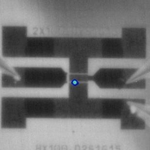
7 Technology Overview Mulifinger devices TEM cross section LETI Gate 100mm 150nm Source 100mm compatible process 0.15µm gate length & 0.1µm underway Bi-layer passivation Multi-finger devices MMIC process compatible with UMS Source bridge 100mm MMIC compatible technology 7

 AlN Interlayer (1 nm) GaN Nid (150 nm) GaN - nid AlN Nucleation (100 nm) SiC")

8 Buffer Layer designed by TCAD DRAIN CURRENT (A/mm) Buffer Layer Role : Ensure the electron confinement in the 2-DEG : High On/Off ratio for optimum transconductance -> high gain and minimum short channel effects PE-CVD passivation Source Gate InAlGaN (6.5 nm) AlN Interlayer (1 nm) GaN Nid (150 nm) GaN - nid AlN Nucleation (100 nm) SiC Substrate ICP-CVD passivation Drain 2DEG 1.E+00 1.E-01 1.E-02 1.E-03 1.E-04 1.E-05 1.E-06 1.E-07 1.E-08 1.E-09 1.E-10 Simulation TCAD GATE VOLTAGE (V) nid GaN in the buffer layer -> No pinch-off 8
9 DRAIN CURRENT (A/mm) Buffer Layer designed by TCAD DRAIN CURRENT (A/mm) Buffer Layer Role : Ensure the electron confinement in the 2-DEG : High On/Off ratio for optimum transconductance -> high gain and minimum short channel effects 1.E+00 1.E-01 1.E+00 1.E-01 Simulation TCAD 1.E-02 1.E-02 1.E-03 1.E-03 1.E-04 1.E-04 G m 1.E-05 1.E-05 1.E-06 1.E-06 1.E-07 1.E-07 1.E-08 1.E-08 1.E-09 1.E-09 1.E GATE VOLTAGE (V) 1.E GATE VOLTAGE (V) Good pinch-off : High Gm 9
 2x50x0.15µm -5-4.5-4 -3.5-3 -2.5-2 -1.")
 Sub-threshold swing of 140mV/dec to 220mV/dec Between 5V and 20V with Ids+ > 1.")
10 Electrical validation of our back-barrier buffer layer Id & Ig (A/mm) Sub-Threshold Swing (mv/dec) Good pinch-off characteristics with our AlGaN Backbarrier with 0.15µm gate length Vgs (V) 2x50x0.15µm E Vds=5V Vds=10V Vds=15V Vds=20V 1.E-01 1.E-02 1.E-03 1.E-04 1.E-05 1.E µm 0.25µm Vds (V) Sub-threshold swing of 140mV/dec to 220mV/dec Between 5V and 20V with Ids+ > 1.2A/mm 10


11 Electrical validation of our back-barrier buffer layer Recovery Time Measurement Bench Hall effet probe Digital Oscilloscope Thermal chuck On wafer probe station AMCAD PIV HP8114A HP81110A 11
 Vgs is kept constant Vds is pulsed : Ids")


12 Buffer designed by TCAD Experimental recovery Time Measurement Id (A) Vgs is kept constant Vds is pulsed : Ids measured using a hall effect probe and digital oscilloscope Stimuli Pulse Vds : 9V à 19V AlGaN/GaN with Fe-doped buffer InAlGaN/GaN with back-barrier Vgs est fixe Vds (V) Our buffer layer incorporating a back-barrier approach significantly reduces the recovery time of drain current in comparison to Fe-doped buffer layer. 12
13 Buffer designed by TCAD Experimental recovery Time Measurement Drain current (A/mm) Comparison with TCAD simulations AlGaN/GaN with Fe-doped buffer InAlGaN/GaN with back-barrier Simulation TCAD SILVACO InAlN_BB AlGaN_Fer time, msec TCAD simulations have well predicted the time domain behavior of the drain current. The time domain signature of the Iron in the buffer layer is well established. 13
 Impact of the back-side")


14 Buffer designed by TCAD Experimental recovery Time Measurement Drain current (A/mm) Impact of the back-side temperature AlGaN/GaN with Fe-doped buffer 30 C 40 C 50 C 60 C 70 C 80 C 90 C 100 C TCAD : The time domain signature of the iron in the buffer layer is well established also versus the temperature Simulation TCAD 30 C 40 C 50 C 60 C 70 C 80 C SILVACO 90 C 100 C time, msec 14


 Same temperature increase")

15 Temperature Increase ( C) Thermal validation of back-barrier buffer layer Raman Measurements performed at TRT TS837_SiC CREE03-04_SiC TS837_GaN CREE03-04_GaN T GaN Fe-doped buffer III-V Lab Back-Barrier buffer T SiC Fe-doped buffer 0 III-V Lab Back-Barrier buffer 0,6 0,7 0,8 0,9 1 1,1 1,2 1,3 1,4 1,5 1,6 1,7 1,8 1,9 2 2,1 Dissipated Power (W) Same temperature increase for Fe-doped buffer layer and backbarrier buffer, A buffer layer thermally optimized and with reduced lagging effects has been developed successfully by III-Vlab. 15

16 Id Id (A) (A/mm) And from the surface Non optimal passivation PASS3 : Bi-layer of SiN Vgsq =0V, Vdsq =0V Vgsq =-5V, Vdsq =0V Vgsq =-5V, Vdsq =25V Vgs = 1 V Vgs = 0 V Vgs = -1 V Vgs = -2 V Vgs = -3 V Vgs = -4 V Vgs = -5 V Our bi-layer passivation approach (PASS3) had significantly reduced lagging effects coming from the surface Vds (V) Reduced lagging effects up Vds q = 25V 16
 Vgs")
17 DC Characteristics : Ids+, Ig leak & gm Gmmax (ms/mm) Vds=10V Vgs=-7V Vds=10V Vgs=+1V Vds=10V TS838W6_2x50D15S8G15V2#C4_m02 (mes2) IgL eak low (<300 µa/mm) Ids+ # 1.2A/mm Igs # 0.2 ma/mm Gm_ext # 450 ms/mm 0207_[18] 0208_[19] 0210_[21] 0307_[30] 0308_[31] 0310_[33] 0407_[42] 0408_[43] 0410_[45] 0507_[54] 0508_[55] 0510_[57] Vgs (V) Vgs (V) Gm (ms/mm)
 AlGaN Patent Pinch-off J K J J Recovery time L K J J Thermal resistance J J L L J III-V Lab have developed a buffer layer thermally")
18 Buffer Layer Buffer Layer Approaches : Acceptor dopant Back-Barrier Iron Carbon AlGaN (Al 8% - 1.6µm) AlGaN Patent Pinch-off J K J J Recovery time L K J J Thermal resistance J J L L J III-V Lab have developed a buffer layer thermally optimized and with reduced lagging effects 18


19 MSG/MAG & H21 ² (db) InAlGaN/GaN 0.15µm [S]-Parameters Small signal figures of merit H21 ² MSG/MAG 10 F (GHz) 20V 200mA/mm 2x50µm x 0.15µm -20dB/dec F t & F MAG # 70 GHz & ma/mm MSG = 30 GHz (probes planes no de-embedding) GHz GHz

20 Load-Pull Measurements Load-pull active/passive bench from S-Band to 30 GHz : Upgrade to 40 GHz in 2018 Active Harmonic matching. HPA1 HPA2 Powered by 20


21 30 GHz CW 6 InAlGaN/GaN HEMT measured : 8x50µm ; Lg=0.15µm Vd = 17.5V ; Ids = 100mA/mm 1.2W power 30 GHz Pout PAE Gp Pout : [ ] PAEmax [ ] W [3-3.5] W/mm MaxPAE : [41-45] % Gp : [ dB PAEmax 21
22 30 GHz CW 0.15µm - 8x50µm InAlGaN/GaN devices 2W/mm 1W 48% 1.4W 45% 2.5W/mm 4.5W/mm 4.5W/mm Optimum load for PAE Jds=50mA/mm Vds=15V Vds=17V Vds=20V Vds=22V Optimum load for Power Jds=50mA/mm Vds=15V Vds=17V Vds=20V Vds=22V 22

23 PAE (%) 10 GHz CW 0.15µm - 6x60µm InAlGaN/GaN devices x60µm F 0 =10 GHz Vds=15V Ids=200mA/mm Γ H2 = 1; φl H2 = 60 H2 optimum H2=50 Ohms ZL Fund for ZL H2 opt ZL Fund for ZL H2 50Ω PAE : up to 80% achieved WITH H2 control on InAlGaN/GaN HEMT devices Pout (dbm) 23
 I DS (V DS )")

24 I DS =8V (%) Vds=8V (%) Some DC stability tests On-wafer DC stability tests DC Life test conditions: V DS =17.5V - 20V; I DS =200mA/mm; 64 h The evolution of the output characteristics is monitored during the test Stable DC parameters (I DSS degradation < 10%) I DS (V DS ) interim measurements 0% 0% -5% I DSS evolution DC Life Test_TS838W6 I DS =200mA/mm & V DS =15V, 17.5V, 20V (2x50µm, Lg=0.15µm) 17.5V, Ta=RT -10% 20V, Ta=RT -15% -20% -20% 15V, Ta=85 C 17.5V_XFD 17.5V_XED 20V_XDP 15V_BYH_a 15V_BXH_b Improvement still needed and on-going -30% Time (h) Passivation identified as not robust enough at high Vds 24-25% - 30% Time (hrs)


25 HPA MMIC Simulations 3 stages [ ] GHz Pout # 40 dbm PAE > 22% 5140x3640µm² Vds=17.5V Ids=200mA/mm Demonstration at circuit level in Ka and Q bands ARCTURUS 28 GHz Simulations 3 stages [ ] GHz Pout # 37 dbm PAE > 15% 5140x3640µm² Vds=17.5V Ids=200mA/mm SIRIUS 38 GHz 25
26 Demonstration at circuit level in Ka and Q bands Pulsed power Vds=17V 800mA 0.2nH On Wafer (50 Ohms) 0.2nH On Wafer (50 Ohms) Up to 10W at 25 GHz PAE > 20% On JIG measurements should improve performances in the upper frequency band 26
27 Demonstration at circuit level in Ka and Q bands Pulsed power Vds=17V 800mA 25dBm 25dBm 27dBm 27dBm 6W at 39.5 GHz with 20% PAE 27
28 Conclusions InAlGaN technology with 0.15µm gate length can operate up to Q-Band Optimized AlGaN back-barrier buffer layer offers disruptive behaviors Thermal and recovery time 100mm process MMIC compatible technology 6W demonstrated at 39.5 GHz at HPA level Robustness improvement is on going 28
29 Acknowledgments The authors would like to thank : the European Defense Agency (EDA) for the support to this work in the context of the project entitled European Gallium Nitride Industry supply Chain (EUGaNIC) funded by Germany, France Italy and Sweden in the frame of the Project n B-1447-IAP1-GP of the European Defence Agency. French Ministry of Economy (DGE) : VEGaN project French MOD (DGA) and CNES And : UMS for MMIC processing and measurements Prof. Juan Obregon for constant technical advices and fruitful discussions 29


30 Thank you for your attention! 30
InAlN/GaN HEMTs Technologies for Microwave, Fast switching and Mixed Signal Applications
 InAlN/GaN HEMTs Technologies for Microwave, Fast switching and Mixed Signal Applications S.DELAGE / S.PIOTROWICZ Summary III-V Lab presentation Motivations Technology for L & S band applications Technology
GaN Technology for Microwave Applications in Ka and Q bands. S. Delage CAPABILITIES AND APPLICATIONS OF GaN DEVICES Microwave and RF 2015
 GaN Technology for Microwave Applications in Ka and Q bands S. Delage CAPABILITIES AND APPLICATIONS OF GaN DEVICES Microwave and RF 2015 R. Aubry, S. Bernard, M. Magis N. Michel, O. Patard, O. Drisse,
Microwave & RF 22 nd of March 2018 D. FLORIOT
 Microwave & RF 22 nd of March 2018 D. FLORIOT Outine Introduction GaN technology roadmap GH15-10 : Up to Ka band GH10 : Towards high frequency (Q / V bands) GaN : Technology & Integration 2 UMS at a glance
GaN MMIC PAs for MMW Applicaitons
 GaN MMIC PAs for MMW Applicaitons Miroslav Micovic HRL Laboratories LLC, 311 Malibu Canyon Road, Malibu, CA 9265, U. S. A. mmicovic@hrl.com Motivation for High Frequency Power sources 6 GHz 11 GHz Frequency
85W Power Transistor. GaN HEMT on SiC
 GaN HEMT on SiC Description The is a 85W Gallium Nitride High Electron Mobility Transistor. This product offers a general purpose and broadband solution for a variety of RF power applications such as radar
100nm GaN on Si: A Pioneering Technology to Enable High RF Power in Millimeter Wave Bands NEW ENGLAND IMAPS SYMPOSIUM MAY 5, 2015
 Innovating with III-V s 100nm GaN on Si: A Pioneering Technology to Enable High RF Power in Millimeter Wave Bands NEW ENGLAND IMAPS SYMPOSIUM MAY 5, 2015 By Dr Fabien ROBERT Sales & Application Team Manager,
Novel III-Nitride HEMTs
 IEEE EDS Distinguished Lecture Boston Chapter, July 6 2005 Novel III-Nitride HEMTs Professor Kei May Lau Department of Electrical and Electronic Engineering Hong Kong University of Science and Technology
III-Nitride microwave switches Grigory Simin
 Microwave Microelectronics Laboratory Department of Electrical Engineering, USC Research Focus: - Wide Bandgap Microwave Power Devices and Integrated Circuits - Physics, Simulation, Design and Characterization
DC - 20 GHz Discrete power phemt
 DC - 20 GHz Discrete power phemt Product Description The TriQuint is a discrete 0.6 mm phemt which operates from DC-20 GHz. The is designed using TriQuint s proven standard 0.3um power phemt production
AlGaN Polarization Graded Field Effect Transistors for High Linearity Microwave Applications
 AlGaN Polarization Graded Field Effect Transistors for High Linearity Microwave Applications Shahadat H. Sohel, Hao Xue, Towhidur Razzak, Sanyam Bajaj, Yuewei Zhang, Wu Lu, Siddharth Rajan Department of
MECXQMM-60W. 8.3 to 10.3 GHz GaN HEMT Power Amplifier
 Pout (dbm), PAE(%) Functional Block Diagram Main Features 0.25µm GaN HEMT Technology 8.3 10.3 GHz full performances Frequency Range 60W Output Power @ Pin 40.5 dbm PAE > 33% @ Pin 40.5 dbm Linear Gain
International Workshop on Nitride Semiconductors (IWN 2016)
") International Workshop on Nitride Semiconductors (IWN 2016) Sheng Jiang The University of Sheffield Introduction The 2016 International Workshop on Nitride Semiconductors (IWN 2016) conference is held
International Workshop on Nitride Semiconductors (IWN 2016) Sheng Jiang The University of Sheffield Introduction The 2016 International Workshop on Nitride Semiconductors (IWN 2016) conference is held
Load Pull Validation of Large Signal Cree GaN Field Effect Transistor (FET) Model
 Model") APPLICATION NOTE Load Pull Validation of Large Signal Cree GaN Field Effect Transistor (FET) Model Introduction Large signal models for RF power transistors, if matched well with measured performance,
APPLICATION NOTE Load Pull Validation of Large Signal Cree GaN Field Effect Transistor (FET) Model Introduction Large signal models for RF power transistors, if matched well with measured performance,
1. INTRODUCTION. Gabriele Formicone Integra Technologies, Inc. 321 Coral Circle El Segundo, CA
 High Efficiency Switch Mode GaN-based Power Amplifiers for P-Band Aerospace Applications James Custer Integra Technologies, Inc. 5072 Hillsdale Circle #120 El Dorado Hills, CA 95762 916-432-3343 jcuster@integratech.com
Advance Datasheet Revision: October Applications
 APN149 Applications Military SatCom Phased-Array Radar Applications Point-to-Point Radio Point-to-Multipoint Communications Terminal Amplifiers Product Description X = 4.4mm Y = 2.28mm Product Features
Advance Datasheet Revision: April 2015
 APN 1-1 GHz Advance Datasheet Revision: April Applications Point-to-Point Digital Radios Point-to-Multipoint Digital Radios VSAT Test Instrumentation X = 3 um Y = 3 um Product Features RF frequency: 1
15W Power Packaged Transistor. GaN HEMT on SiC
 Gain (db), Pout (dbm) & PAE (%) Drain Current (A) CHK15A-QIA Description The CHK15A-QIA is an unmatched packaged Gallium Nitride High Electron Mobility Transistor. It offers general purpose and broadband
NPA100-D GHz GaN 20W Power Amplifier. Product Description: Key Features:
 Product Description: The Nxbeam is a Ku-band high power GaN MMIC fabricated in 0.2um GaN HEMT on SiC. This part is ideally suited for satellite communications, point-to-point radios, and radar applications.
PRELIMINARY = 25 C) Parameter GHz 14.0 GHz 14.5 GHz Units Small Signal Gain db P SAT. = 26 dbm W P 3dB
 Parameter GHz 14.0 GHz 14.5 GHz Units Small Signal Gain db P SAT. = 26 dbm W P 3dB") CMPADE030D PRELIMINARY 30 W, 3.75-4.5 GHz, 40 V, GaN MMIC, Power Amplifier Cree s CMPADE030D is a gallium nitride (GaN) High Electron Mobility Transistor (HEMT) based monolithic microwave integrated circuit
CMPADE030D PRELIMINARY 30 W, 3.75-4.5 GHz, 40 V, GaN MMIC, Power Amplifier Cree s CMPADE030D is a gallium nitride (GaN) High Electron Mobility Transistor (HEMT) based monolithic microwave integrated circuit
25W Power Packaged Transistor. GaN HEMT on SiC
 25W Power Packaged Transistor GaN HEMT on SiC Description The is an unmatched packaged Gallium Nitride High Electron Mobility Transistor. It offers general purpose and broadband solutions for a variety
Ph.D. Defense. Broadband Power Amplifier
 Ph.D. Defense GaN HEMTs based Flip-chip Integrated Broadband Power Amplifier Jane Xu University of California at Santa Barbara Committee: Prof. Stephen Long Prof. Umesh Mishra Dr. Yi-feng Wu Prof. Bob
NPA105-D. Preliminary GHz GaN 40W Power Amplifier. Product Description: Key Features:
 Product Description: The Nxbeam is a Ku-band high power GaN MMIC fabricated in 0.2um GaN HEMT on SiC. This part is ideally suited for satellite communications, point-to-point radios, and radar applications.
Advance Datasheet Revision: May 2013
 Applications Military SatCom Phased-Array Radar Applications Point-to-Point Radio Point-to-Multipoint Communications Terminal Amplifiers X = 4.4mm Y = 2.28mm Product Features RF frequency: 18 to 23 GHz
NPA110-D. Preliminary GHz GaN 38W Power Amplifier. Product Description: Key Features:
 NPA1-D Product Description: The Nxbeam NPA1-D is a Ka-band high power GaN MMIC fabricated in.2um GaN HEMT on SiC. This part is ideally suited for satellite communications, point-to-point radios, and radar
MECGaNC30. 4 to 6 GHz GaN HEMT Power Amplifier. Main Features. Product Description. Applications
 Main Features 0.25µm GaN HEMT Technology 4.1 5.9 GHz full performances Frequency Range W Output Power @ Pin 27.5 dbm 37% PAE @ Pin 27.5 dbm % PAE @ Pout Watt 27 db Small Signal Gain Product Description
40W Power Packaged Transistor. GaN HEMT on SiC
 Gain (db), Pout (dbm) & PAE (%) Id (A) Description 40W Power Packaged Transistor The is an unmatched packaged Gallium Nitride High Electron Mobility Transistor. It offers general purpose and broadband
Gallium nitride (GaN)
") 80 Technology focus: GaN power electronics Vertical, CMOS and dual-gate approaches to gallium nitride power electronics US research company HRL Laboratories has published a number of papers concerning
80 Technology focus: GaN power electronics Vertical, CMOS and dual-gate approaches to gallium nitride power electronics US research company HRL Laboratories has published a number of papers concerning
PRELIMINARY DATASHEET
 PRELIMINARY DATASHEET 8-12 GHz 41dBm Power Amplifier DESCRIPTION The is a high performance dual line-up 3 stages GaAs Power Amplifier MMIC designed to operate in the X band. The has an output power of
= 25 C) Parameter 2.7 GHz 2.9 GHz 3.1 GHz 3.3 GHz 3.5 GHz Units Small Signal Gain db
 Parameter 2.7 GHz 2.9 GHz 3.1 GHz 3.3 GHz 3.5 GHz Units Small Signal Gain db") CMPA273575D 75 W, 2.7-3.5 GHz, GaN MMIC, Power Amplifier Cree s CMPA273575D is a gallium nitride (GaN) High Electron Mobility Transistor (HEMT) based monolithic microwave integrated circuit (MMIC). GaN
CMPA273575D 75 W, 2.7-3.5 GHz, GaN MMIC, Power Amplifier Cree s CMPA273575D is a gallium nitride (GaN) High Electron Mobility Transistor (HEMT) based monolithic microwave integrated circuit (MMIC). GaN
Customized probe card for on-wafer testing of AlGaN/GaN power transistors
 Customized probe card for on-wafer testing of AlGaN/GaN power transistors R. Venegas 1, K. Armendariz 2, N. Ronchi 1 1 imec, 2 Celadon Systems Inc. Outline Introduction GaN for power switching applications
= 25 C) Parameter 8.0 GHz 9.0 GHz 10.0 GHz 11.0 GHz Units Small Signal Gain db P OUT. = 25 dbm W Power P IN
 Parameter 8.0 GHz 9.0 GHz 10.0 GHz 11.0 GHz Units Small Signal Gain db P OUT. = 25 dbm W Power P IN") CMPA80B05D 5 W, 8.0 -.0 GHz, GaN MMIC, Power Amplifier Cree s CMP80B05D is a gallium nitride (GaN) High Electron Mobility Transistor (HEMT) based monolithic microwave integrated circuit (MMIC). GaN has
CMPA80B05D 5 W, 8.0 -.0 GHz, GaN MMIC, Power Amplifier Cree s CMP80B05D is a gallium nitride (GaN) High Electron Mobility Transistor (HEMT) based monolithic microwave integrated circuit (MMIC). GaN has
Preliminary Datasheet Revision: January 2016
 Preliminary Datasheet Revision: January 216 Applications Point-to-Point Digital Radios Point-to-Multipoint Digital Radios SATCOM Terminals X = 3.65mm Y = 2.3mm Product Features RF frequency: 27 to 31 GHz
6-18 GHz High Power Amplifier TGA9092-SCC
 6-18 GHz High Power Amplifier Key Features and Performance Dual Channel Power Amplifier 0.25um phemt Technology 6-18 GHz Frequency Range 2.8 W/Channel Midband Pout 5.6 W Pout Combined 24 db Nominal Gain
Pulse IV and pulsed S-parameter Parametric Analysis with AMCAD PIV & AGILENT PNA-X
 Pulse IV and pulsed S-parameter Parametric Analysis with AMCAD PIV & AGILENT PNA-X Tony Gasseling gasseling@amcad-engineering.com 1 Components PA Design Flow Measurement system Measurement Data base Circuits
Customized probe card for on wafer testing of AlGaN/GaN power transistors
 Customized probe card for on wafer testing of AlGaN/GaN power transistors R. Venegas 1, K. Armendariz 2, N. Ronchi 1 1 imec, 2 Celadon Systems Inc. Presented by Bryan Root 2 Outline Introduction GaN for
ARFTG Workshop, Boulder, December 2014
 ARFTG Workshop, Boulder, December 2014 Design and measurements of high-efficiency PAs with high PAR signals Zoya Popovic, Tibault Reveyrand, David Sardin, Mike Litchfield, Scott Schafer, Andrew Zai Department
ULTRA LOW NOISE PSEUDOMORPHIC HJ FET
 ULTRA LOW NOISE PSEUDOMORPHIC HJ FET NE34 FEATURES VERY LOW NOISE FIGURE: NF =.6 db typical at f = GHz HIGH ASSOCIATED GAIN: GA =. db typical at f = GHz LG =.5 µm, WG = µm DESCRIPTION The NE34 is a pseudomorphic
GaN/SiC Bare Die Power HEMT DC-15 GHz
 GaN/SiC Bare Die Power HEMT DC-15 GHz DESCRIPTION AMCOM s is a discrete GaN/SiC HEMT that has a total gate width of mm (Eight 1.mm FETs in parallel). It is a bare die which can be operated up to 15 GHz.
= 25 C) Parameter 5.5 GHz 6.5 GHz 7.5 GHz 8.5 GHz Units Small Signal Gain db P OUT
 Parameter 5.5 GHz 6.5 GHz 7.5 GHz 8.5 GHz Units Small Signal Gain db P OUT") CMPA5585030D 30 W, 5.5-8.5 GHz, GaN MMIC, Power Amplifier Cree s CMPA5585030D is a gallium nitride (GaN) High Electron Mobility Transistor (HEMT) based monolithic microwave integrated circuit (MMIC). GaN
CMPA5585030D 30 W, 5.5-8.5 GHz, GaN MMIC, Power Amplifier Cree s CMPA5585030D is a gallium nitride (GaN) High Electron Mobility Transistor (HEMT) based monolithic microwave integrated circuit (MMIC). GaN
GaN/SiC Bare Die Power HEMT DC-15 GHz
 GaN/SiC Bare Die Power HEMT DC-15 GHz DESCRIPTION AMCOM s is a discrete GaN/SiC HEMT that has a total gate width of 5mm (Four 1.mm FETs in parallel). It is a bare die which can be operated up to 15 GHz.
GaN: Applications: Optoelectronics
 GaN: Applications: Optoelectronics GaN: Applications: Optoelectronics - The GaN LED industry is >10 billion $ today. - Other optoelectronic applications of GaN include blue lasers and UV emitters and detectors.
AlGaN/GaN HEMTs and HBTs
 AlGaN/GaN HEMTs and HBTs Umesh K. Mishra PART I AlGaN/GaN HEMTs Materials Properties Comparison Material µ ε Eg BFOM JFM Tmax Ratio Ratio Si 1300 11.4 1.1 1.0 1.0 300 C GaAs 5000 13.1 1.4 9.6 3.5 300 C
ATF Enhancement Mode [1] Pseudomorphic HEMT in SOT 89 Package
![ATF Enhancement Mode [1] Pseudomorphic HEMT in SOT 89 Package](/thumbs/86/93207835.jpg "ATF Enhancement Mode [1] Pseudomorphic HEMT in SOT 89 Package") ATF-3189 Enhancement Mode [1] Pseudomorphic HEMT in SOT 89 Package Data Sheet Description Avago Technologies s ATF-3189 is a single-voltage high linearity, low noise E-pHEMT FET packaged in a low cost
ATF-3189 Enhancement Mode [1] Pseudomorphic HEMT in SOT 89 Package Data Sheet Description Avago Technologies s ATF-3189 is a single-voltage high linearity, low noise E-pHEMT FET packaged in a low cost
= 25 C) Parameter 6.0 GHz 7.5 GHz 9.0 GHz 10.5 GHz 12.0 GHz Units Small Signal Gain db P OUT
 Parameter 6.0 GHz 7.5 GHz 9.0 GHz 10.5 GHz 12.0 GHz Units Small Signal Gain db P OUT") CMPA601C025F 25 W, 6.0-12.0 GHz, GaN MMIC, Power Amplifier The CMPA601C025F is a gallium nitride (GaN) High Electron Mobility Transistor (HEMT) based monolithic microwave integrated circuit (MMIC) on a
CMPA601C025F 25 W, 6.0-12.0 GHz, GaN MMIC, Power Amplifier The CMPA601C025F is a gallium nitride (GaN) High Electron Mobility Transistor (HEMT) based monolithic microwave integrated circuit (MMIC) on a
= 25 C) Parameter 1.0 GHz 2.0 GHz 3.0 GHz 4.0 GHz 5.0 GHz 6.0 GHz Units. Gain db. 32 dbm W
 Parameter 1.0 GHz 2.0 GHz 3.0 GHz 4.0 GHz 5.0 GHz 6.0 GHz Units. Gain db. 32 dbm W") CMPA006005D 5 W, 0 MHz - 6.0 GHz, GaN MMIC, Power Amplifier Cree s CMPA006005D is a gallium nitride (GaN) High Electron Mobility Transistor (HEMT) based monolithic microwave integrated circuit (MMIC).
CMPA006005D 5 W, 0 MHz - 6.0 GHz, GaN MMIC, Power Amplifier Cree s CMPA006005D is a gallium nitride (GaN) High Electron Mobility Transistor (HEMT) based monolithic microwave integrated circuit (MMIC).
GaN Technologies Applications, Status and Trends
 GaN Technologies Applications, Status and Trends Didier Floriot 2, Hervé Blanck 1, Reza Behtash 1, Franck Bourgeois 1, Peter Brückner 1, Marc Camiade 2, Laurent Favede 2, Sylvain Heckmann 1, Helmut Jung
Fundamental Failure Mechanisms Limiting Maximum Voltage Operation in AlGaN/GaN HEMTs. Michael D. Hodge, Ramakrishna Vetury, and Jeffrey B.
 Fundamental Failure Mechanisms Limiting Maximum Voltage Operation in AlGaN/GaN HEMTs Michael D. Hodge, Ramakrishna Vetury, and Jeffrey B. Shealy Purpose Propose a method of determining Safe Operating Area
= 25 C) Parameter 0.5 GHz 1.0 GHz 2.5 GHz 4.0 GHz 6.0 GHz Units. Gain db. 23 dbm W
 Parameter 0.5 GHz 1.0 GHz 2.5 GHz 4.0 GHz 6.0 GHz Units. Gain db. 23 dbm W") CMPA6D Watt, MHz - 6 MHz GaN HEMT MMIC Power Amplifier Cree s CMPA6D is a gallium nitride (GaN) High Electron Mobility Transistor (HEMT) based monolithic microwave integrated circuit (MMIC). GaN has superior
CMPA6D Watt, MHz - 6 MHz GaN HEMT MMIC Power Amplifier Cree s CMPA6D is a gallium nitride (GaN) High Electron Mobility Transistor (HEMT) based monolithic microwave integrated circuit (MMIC). GaN has superior
GaN power electronics
 GaN power electronics The MIT Faculty has made this article openly available. Please share how this access benefits you. Your story matters. Citation As Published Publisher Lu, Bin, Daniel Piedra, and
TEST FREQ. 12 GHz 18 GHz 12 GHz 18 GHz. P1dB Output p1db (Vds = 2V, Id = 10mA) 12 GHz dbm
 12 GHz dbm") SUPER LOW NOISE PHEMT CHIP (.15µm x 160µm) The BeRex BCL016B is a GaAs super low noise phemt with a nominal 0.15 micron gate length and 160 micron gate width making the product ideally suited for applications
SUPER LOW NOISE PHEMT CHIP (.15µm x 160µm) The BeRex BCL016B is a GaAs super low noise phemt with a nominal 0.15 micron gate length and 160 micron gate width making the product ideally suited for applications
Stuart Glynn Power Amplifier Design Engineer
 Stuart Glynn Power Amplifier Design Engineer Keysight Technologies 2017 How to Design an X-band MMIC PA Stuart Glynn and Liam Devlin Introduction Target specification and application Design approach Device
10W Ultra-Broadband Power Amplifier
 (TH1B-01 ) 10W Ultra-Broadband Power Amplifier Amin K. Ezzeddine and Ho. C. Huang AMCOM Communications, Inc 401 Professional Drive, Gaithersburg, MD 20879, USA Tel: 301-353-8400 Email: amin@amcomusa.com
= 25 C) Parameter 0.5 GHz 1.0 GHz 2.5 GHz 4.0 GHz 6.0 GHz Units. Gain db. 23 dbm W
 Parameter 0.5 GHz 1.0 GHz 2.5 GHz 4.0 GHz 6.0 GHz Units. Gain db. 23 dbm W") CMPA0060002D 2 Watt, MHz - 6000 MHz GaN HEMT MMIC Power Amplifier Cree s CMPA0060002D is a gallium nitride (GaN) High Electron Mobility Transistor (HEMT) based monolithic microwave integrated circuit (MMIC).
CMPA0060002D 2 Watt, MHz - 6000 MHz GaN HEMT MMIC Power Amplifier Cree s CMPA0060002D is a gallium nitride (GaN) High Electron Mobility Transistor (HEMT) based monolithic microwave integrated circuit (MMIC).
Design of Enhancement Mode Single-gate and Double-gate Multi-channel GaN HEMT with Vertical Polarity Inversion Heterostructure
 MITSUBISHI ELECTRIC RESEARCH LABORATORIES http://www.merl.com Design of Enhancement Mode Single-gate and Double-gate Multi-channel GaN HEMT with Vertical Polarity Inversion Heterostructure Feng, P.; Teo,
5W X Band Medium Power Amplifier. GaN Monolithic Microwave IC
 GaN Monolithic Microwave IC Description V+ The CHA6710-99F is a two stage Medium Power Amplifier operating between 8.0 and 12.75GHz. It typically provides 5W of saturated output power and 36% of power
MwT-1789SB GHz Packaged FET
 Features: Designed for single voltage operations Ideal for 0.5 4.0 GHz High Linearity / High Dynamic Range Applications Excellent RF Performance: o 44 dbm IP3 o 65 dbc ACPR o 28 dbm P1dB o 18 db SSG @
Product Datasheet Revision: January 2015
 Applications Short Haul / High Capacity Links Sensors X=23 mm Y=16 mm Product Features RF Frequency: 92 to 96 GHz Linear Gain: 7.5 db typ. Psat: 25 dbm typ. Die Size: 3.7 sq. mm. 2 mil substrate DC Power:
Investigations on Compound Semiconductor High Electron Mobility Transistor (HEMT)
") Investigations on Compound Semiconductor High Electron Mobility Transistor (HEMT) Nov. 26, 2004 Outline I. Introduction: Why needs high-frequency devices? Why uses compound semiconductors? How to enable
Investigations on Compound Semiconductor High Electron Mobility Transistor (HEMT) Nov. 26, 2004 Outline I. Introduction: Why needs high-frequency devices? Why uses compound semiconductors? How to enable
GaN based Power Devices. Michael A. Briere. RPI CFES Conference
 GaN based Power Devices Michael A. Briere ACOO Enterprises LLC Under contract to International Rectifier RPI CFES Conference January 25, 2013 1 Motivation : Potential Energy Savings Worldwide M.A. Briere
18W X-Band High Power Amplifier. GaN Monolithic Microwave IC
 CHA8611-99F GaN Monolithic Microwave IC Description V+ The CHA8611-99F is a two stage High Power Amplifier operating between 8.5 and 11GHz and providing typically 18W of saturated output power and 43%
Defense Technical Information Center Compilation Part Notice
 UNCLASSIFIED Defense Technical Information Center Compilation Part Notice ADP015074 TITLE: Channel Recessed 4H-SiC MESFETs with Ft o f14.5ghz and F max of 40GHz DISTRIBUTION: Approved for public release,
GRADE Graphene-based Devices and Circuits for RF Applications Collaborative Project
 GRADE Graphene-based Devices and Circuits for RF Applications Collaborative Project WP 6 D6.1 DC, S parameter and High Frequency Noise Characterisation of GFET devices Main Authors: Sebastien Fregonese,
PH9 Reliability. Application Note # 51 - Rev. A. MWTC MARKETING March 1997
 PH9 Reliability Application Note # 51 - Rev. A MWTC MARKETING March 1997 1.0. Introduction This application note provides a summary of reliability and environmental testing performed to date on 0.25 µm
Advance Datasheet Revision: January 2015
 Advance Datasheet Revision: January 215 Applications Military SatCom Phased-Array Radar Applications Terminal Amplifiers X = 3.7mm Y = 3.2mm Product Features RF frequency: 43 to 46 GHz Linear Gain: 2 db
A new nonlinear HEMT model allowing accurate simulation of very low IM 3 levels for high-frequency highly linear amplifiers design
 A new nonlinear HEMT model allowing accurate simulation of very low IM 3 levels for high-frequency highly linear amplifiers design J. Lhortolary 1, C. Chang 1, T. Reveyrand 2, M. Camiade 1, M. Campovecchio
TGF Watt Discrete Power GaN on SiC HEMT. Key Features. Primary Applications Defense & Aerospace Broadband Wireless. Product Description
 50 Watt Discrete Power GaN on SiC HEMT Key Features Frequency Range: DC - 18 GHz 47 dbm Nominal Psat 55% Maximum PAE 8.7 db Nominal Power Gain Bias: Vd = 28-35 V, Idq = 1 A, Vg = -3.6 V Typical Technology:
PRELIMINARY DATASHEET
 PRELIMINARY DATASHEET 8-12 GHz 41dBm Power Amplifier DESCRIPTION The is a high performance dual line-up 3 stages GaAs Power Amplifier MMIC designed to operate in the X band. The has an output power of
Gallium Nitride & Related Wide Bandgap Materials and Devices
 Gallium Nitride & Related Wide Bandgap Materials and Devices Dr. Edgar J. Martinez Program Manager DARPATech 2000 GaAs IC Markets 1999 Market $11 Billion 2005 Market $20 Billion Consumers 2% Computers
& ) > 35W, 33-37% PAE
 > 35W, 33-37% PAE") Outline Status of Linear and Nonlinear Modeling for GaN MMICs Presented at IMS11 June, 11 Walter R. Curtice, Ph. D. Consulting www.curtice.org State of the Art Modeling considerations, types of models,
Outline Status of Linear and Nonlinear Modeling for GaN MMICs Presented at IMS11 June, 11 Walter R. Curtice, Ph. D. Consulting www.curtice.org State of the Art Modeling considerations, types of models,
LOW NOISE L TO K-BAND GaAs MESFET SYMBOLS PARAMETERS AND CONDITIONS UNITS MIN TYP MAX NFOPT 1
 FEATURES LOW NOISE FIGURE NF = 1.6 db TYP at f = 1 GHz HIGH ASSOCIATED GAIN GA = 9.5 db TYP at f = 1 GHz LG = 0.3 µm, WG = 80 µm EPITAXIAL TECHNOLOGY LOW PHASE NOISE DESCRIPTION The features a low noise
Development of Microwave and Terahertz Detectors Utilizing AlN/GaN High Electron Mobility Transistors
 Development of Microwave and Terahertz Detectors Utilizing AlN/GaN High Electron Mobility Transistors L. Liu 1, 2,*, B. Sensale-Rodriguez 1, Z. Zhang 1, T. Zimmermann 1, Y. Cao 1, D. Jena 1, P. Fay 1,
Product Data Sheet August 5, 2008
 TriQuint Recommends the TGA4516 be used for New Designs 33-36 GHz 2W Power Amplifier Key Features 0.25 um phemt Technology 17 db Nominal Gain 31 dbm Pout @ P1dB, Psat 33dBm @ 6V, 34dBm @7V Bias 6-7V @
FABRICATION OF SELF-ALIGNED T-GATE AlGaN/GaN HIGH
 International Journal of High Speed Electronics and Systems World Scientific Vol. 14, No. 3 (24) 85-89 wworldscientific World Scientific Publishing Company www.worldsclentific.com FABRICATION OF SELF-ALIGNED
Reliability Investigation of GaN HEMTs for MMICs Applications
 Micromachines 2014, 5, 570-582; doi:10.3390/mi5030570 Article OPEN ACCESS micromachines ISSN 2072-666X www.mdpi.com/journal/micromachines Reliability Investigation of GaN HEMTs for MMICs Applications Alessandro
FP Description. Features. Applications. Packaging Information. 340W, 48V GaN HEMT D
 FP48005340 340W, 48V GaN HEMT D Description The FP48005340 is a 340W gallium nitride (GaN) High Electron Mobility Transistor (HEMT). This GaN HEMT is a wideband transistor optimized for 3.5GHz operation
FP Description. Features. Applications. Packaging Information. 260W, 48V GaN HEMT D
 FP48005260 260W, 48V GaN HEMT D Description The FP48005260 is a 260W gallium nitride (GaN) High Electron Mobility Transistor (HEMT). This GaN HEMT is a wideband transistor optimized for 3.5GHz operation
FP Description. Features. Applications. Packaging Information. 50W, 28V GaN HEMT Die
 FP28010060 50W, 28V GaN HEMT Die Description The FP28010060 is a 50W gallium nitride (GaN) High Electron Mobility Transistor (HEMT). This GaN HEMT is a wideband transistor optimized for X-band operation
TGF Watt Discrete Power GaN on SiC HEMT. Key Features. Measured Performance. Primary Applications Space Military Broadband Wireless
 6 Watt Discrete Power GaN on SiC HEMT Key Features Frequency Range: DC - 18 GHz > 38 dbm Nominal Psat 55% Maximum PAE 15 db Nominal Power Gain Bias: Vd = 28-40 V, Idq = 125 ma, Vg = -3 V Typical Technology:
FP Description. Features. Applications. Packaging Information. 104W, 48V GaN HEMT D
 FP48007104 104W, 48V GaN HEMT D Description The FP48007104 is a 104W gallium nitride (GaN) High Electron Mobility Transistor (HEMT). This GaN HEMT is a wideband transistor optimized for 3.5GHz operation
Features. Specifications. Applications
 ATF-531P8 High Linearity Enhancement Mode [1] Pseudomorphic HEMT in 2x2 mm 2 LPCC [3] Package Data Sheet Description Avago Technologies ATF 531P8 is a single-voltage high linearity, low noise E phemt housed
= 25 C) Parameter 2.5 GHz 4.0 GHz 6.0 GHz Units Gain db W Power P OUT. = 43 dbm
 Parameter 2.5 GHz 4.0 GHz 6.0 GHz Units Gain db W Power P OUT. = 43 dbm") CMPA2560025D 25 W, 2.5-6.0 GHz, GaN MMIC, Power Amplifier Cree s CMP2560025D is a gallium nitride (GaN) High Electron Mobility Transistor (HEMT) based monolithic microwave integrated circuit (MMIC). GaN
CMPA2560025D 25 W, 2.5-6.0 GHz, GaN MMIC, Power Amplifier Cree s CMP2560025D is a gallium nitride (GaN) High Electron Mobility Transistor (HEMT) based monolithic microwave integrated circuit (MMIC). GaN
Data Sheet 0GX. ATF Enhancement Mode [1] Pseudomorphic HEMT in SOT 89 Package. Features. Description. Specifications
![Data Sheet 0GX. ATF Enhancement Mode [1] Pseudomorphic HEMT in SOT 89 Package. Features. Description. Specifications](/thumbs/84/90611572.jpg "Data Sheet 0GX. ATF Enhancement Mode [1] Pseudomorphic HEMT in SOT 89 Package. Features. Description. Specifications") ATF-5189 Enhancement Mode [1] Pseudomorphic HEMT in SOT 89 Package Data Sheet Description Avago Technologies s ATF-5189 is a high linearity, medium power, low noise E-pHEMT FET packaged in a low cost surface
ATF-5189 Enhancement Mode [1] Pseudomorphic HEMT in SOT 89 Package Data Sheet Description Avago Technologies s ATF-5189 is a high linearity, medium power, low noise E-pHEMT FET packaged in a low cost surface
MMA GHz 4W MMIC Power Amplifier Data Sheet
 Features: Frequency Range: 27 33 GHz P1dB: +36 dbm IM3 Level: -38 dbc @Po=20dBm/tone Gain: 22 db Vdd = 6V Idsq = 1500 to 2800mA Input and Output Fully Matched to 50 1 2 3 4 5 32 31 30 29 28 27 26 25 24
TGF um Discrete GaAs phemt
 Applications Defense & Aerospace High-Reliability Test and Measurement Commercial Broadband Wireless Product Features Functional Block Diagram Frequency Range: DC - 20 GHz 29.5 dbm Typical Output Power
8Fx. Data Sheet ATF Low Noise Enhancement Mode Pseudomorphic HEMT in a Surface Mount Plastic Package. Description. Features.
 ATF-58143 Low Noise Enhancement Mode Pseudomorphic HEMT in a Surface Mount Plastic Package Data Sheet Description Avago Technologies ATF-58143 is a high dynamic range, low noise E-PHEMT housed in a 4-lead
Overview of the KORRIGAN project
 Overview of the KORRIGAN project Key Organisation for Research in Integrated Circuits in GaN Technology Authors: Philippe Duême (SLIE), Thales Airborne Systems _ France, Andrew Phillips, WP leader (System
CMPA1D1E025F. 25 W, GHz, 40 V, Ku-Band GaN MMIC, Power Amplifier. Typical Performance Over GHz (T C. Features.
 CMPA1D1E025F 25 W, 13.75-14.5 GHz, 40 V, Ku-Band GaN MMIC, Power Amplifier Cree s CMPA1D1E025F is a gallium nitride (GaN) High Electron Mobility Transistor (HEMT) based monolithic microwave integrated
E-PHEMT GHz. Ultra Low Noise, Low Current
 Ultra Low Noise, Low Current E-PHEMT 0.45-6GHz Product Features Low Noise Figure, 0.5 db Gain, 16 db at 2 GHz High Output IP3, + dbm Low Current, ma Wide bandwidth External biasing and matching required
An X-band GaN combined solid-state power amplifier
 Vol. 30, No. 9 Journal of Semiconductors September 2009 An X-band GaN combined solid-state power amplifier Chen Chi( 陈炽 ), Hao Yue( 郝跃 ), Feng Hui( 冯辉 ), Yang Linan( 杨林安 ), Ma Xiaohua( 马晓华 ), Duan Huantao(
Data Sheet 2GX. ATF High Linearity Mode [1] Enhancement Pseudomorphic HEMT in SOT 89 Package. Features. Description.
![Data Sheet 2GX. ATF High Linearity Mode [1] Enhancement Pseudomorphic HEMT in SOT 89 Package. Features. Description.](/thumbs/89/98073316.jpg "Data Sheet 2GX. ATF High Linearity Mode [1] Enhancement Pseudomorphic HEMT in SOT 89 Package. Features. Description.") ATF-2189 High Linearity Mode [1] Enhancement Pseudomorphic HEMT in SOT 89 Package Data Sheet Description Avago Technologies s ATF-2189 is a single-voltage high linearity, low noise E-pHEMT FET packaged
ATF-2189 High Linearity Mode [1] Enhancement Pseudomorphic HEMT in SOT 89 Package Data Sheet Description Avago Technologies s ATF-2189 is a single-voltage high linearity, low noise E-pHEMT FET packaged
PRELIMINARY DATASHEET
 PRELIMINARY DATASHEET 27.5-31 GHz 37dBm High Power Amplifier DESCRIPTION The is a high performance GaAs Power Amplifier MMIC designed to operate in the Ka Band. The has an output power of 4W at the 1dB
Effects of Source Field Plate and Pt- gate Metalliza8on on AlGaN/GaN HEMTs Reliability
 Effects of Source Field Plate and Pt- gate Metalliza8on on AlGaN/GaN HEMTs Reliability Robert Finch, Lu Liu, Chien- Fong Lo, Tsung- Sheng Kang, David A. Cullen, Jinhyung Kim, David. J. Smith, S. J. Pearton
PRELIMINARY. Parameter 500 MHz 1.0 GHz 1.5 GHz 2.0 GHz 2.5 GHz Units. Small Signal Gain db
 CGH49PP 9 W, RF Power GaN HEMT PRELIMINARY Cree s CGH49PP is an unmatched, gallium nitride (GaN) high electron mobility transistor (HEMT). The CGH49PP, operating from a 28 volt rail, offers a general purpose,
TGF Watt Discrete Power GaN on SiC HEMT. Key Features. Measured Performance. Primary Applications Space Military Broadband Wireless
 12 Watt Discrete Power GaN on SiC HEMT Key Features Frequency Range: DC - 18 GHz > 41 dbm Nominal Psat 55% Maximum PAE 15 db Nominal Power Gain Bias: Vd = 28-40 V, Idq = 250 ma, Vg = -3 V Typical Technology:
C Band High Power Amplifier. GaAs Monolithic Microwave IC
 GaAs Monolithic Microwave IC Description is a monolithic two-stage GaAs High Power Amplifier (HPA) designed for C band applications. The HPA provides typically 12W of output power on the 5.2 to 6.0GHz
MMA M GHz 4W MMIC Power Amplifier Data Sheet
 Features: Frequency Range: 27 33 GHz P1dB: +36 dbm IM3 Level: -38 dbc @Po=20dBm/tone Gain: 22 db Vdd = 6V Idsq = 1500 to 2800mA Input and Output Fully Matched to 50 Ω Surface Mount, RoHs Compliant QFN
Data Sheet ATF-511P8. High Linearity Enhancement Mode [1] Pseudomorphic HEMT in 2x2 mm 2 LPCC [3] Package. 1Px. Features.
![Data Sheet ATF-511P8. High Linearity Enhancement Mode [1] Pseudomorphic HEMT in 2x2 mm 2 LPCC [3] Package. 1Px. Features.](/thumbs/84/89103363.jpg "Data Sheet ATF-511P8. High Linearity Enhancement Mode [1] Pseudomorphic HEMT in 2x2 mm 2 LPCC [3] Package. 1Px. Features.") ATF-511P8 High Linearity Enhancement Mode [1] Pseudomorphic HEMT in 2x2 mm 2 LPCC [3] Package Data Sheet Description Avago Technologies s ATF-511P8 is a single-voltage high linearity, low noise E-pHEMT
ATF-511P8 High Linearity Enhancement Mode [1] Pseudomorphic HEMT in 2x2 mm 2 LPCC [3] Package Data Sheet Description Avago Technologies s ATF-511P8 is a single-voltage high linearity, low noise E-pHEMT
Gallium Nitride MMIC Power Amplifier
 Gallium Nitride MMIC Power Amplifier August 2015 Rev 4 DESCRIPTION AMCOM s is an ultra-broadband GaN MMIC power amplifier. It has 21dB gain, and >41dBm output power over the 0.03 to 6GHz band. This MMIC
RADIATION RESPONSE AND RELIABILITY OF HIGH SPEED AlGaN/GaN HEMTS
 RADIATION RESPONSE AND RELIABILITY OF HIGH SPEED AlGaN/GaN HEMTS By Jin Chen Dissertation Submitted to the Faculty of the Graduate school of Vanderbilt University in partial fulfillment of the requirements
AlGaN/GaN HEMTs and HBTs
 AlGaN/GaN HEMTs and HBTs Umesh K. Mishra PART I AlGaN/GaN HEMTs Materials Properties Comparison Material µ ε Eg BFOM JFM Tmax Ratio Ratio Si 1300 11.4 1.1 1.0 1.0 300 C GaAs 5000 13.1 1.4 9.6 3.5 300 C