Pulse IV and pulsed S-parameter Parametric Analysis with AMCAD PIV & AGILENT PNA-X
|
|
|
- Cecilia Whitehead
- 5 years ago
- Views:
Transcription
1 Pulse IV and pulsed S-parameter Parametric Analysis with AMCAD PIV & AGILENT PNA-X Tony Gasseling 1


2 Components PA Design Flow Measurement system Measurement Data base Circuits Prototypes Simulation & design Equivalent models


3 Design Flow Solutions and tools for semiconductor professionals Pulsed IV/ RF meas. VNA Load-Pull meas. Component Model extraction STAN TOOL Design, Stability Analysis, Behavioral Modeling System LP system Circuit PIV-RF system Modelling tool (FET) IVCAD software platform

4 Pulsed measurements Pulsed IV measurements Pulsed S parameter measurements


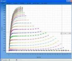
5 Pulsed measurements The quiescent bias point defines the thermal state of the transistor under state. In both cases, using a low duty cycle pulse waveform, typically around 1% or less is used to minimize the energy dissipated in the device under test. Even if low duty cycle are necessary, it is also important to provide short pulses to avoid self-heating during the pulse. Quiescent bias point Temperature increase of AlGaN/GaN HEMTs (SiC substrate), with a chuck temperature of 0 C.
6 Pulsed measurements Electro-thermal measurement Chip temperature Chip temperature DC bias Not only the impulse width, but also the impulse repetition affects self-heating DC bias time time
7 Pulsed measurements Advantages of pulsed IV measurements: High power dissipated areas // safe operating conditions Thermal effects : influence of QP on Idss Trapping effects (gate lag, drain lag) Precious modelling data inputs

8 Pulsed measurements Ideal World PIV Meas. Transistor Characteristic DUT PIV Input PIV Output


9 Pulsed measurements Real World : PIV Meas. Parasitic inductance Parasitic Resistance IV Calibration Transistor Characteristic Bias T Bias T 50W DUT 50W Impedance Stabilization Network PIV Input PIV Output

10 Pulsed measurements Real World for pulsed measurements :

11 Pulsed measurements Real World for pulsed measurements : VOUT IOUT Z=0.5W Ic R L=0 C=0

12 Pulsed measurements Pulsed S parameter measurements Why? How?

13 Pulsed measurements Pulsed S parameter are used for the Extraction of linear model
14 Pulsed measurements Dynamic measurements from a quiescent bias point Starting point of the pulses is the quiescent bias point (Vgs0,Vds0) that defines the thermal and trapping state of the device Small-signal RF during the steady state of the pulses


15 Pulsed measurements Pulsed RF Measurement and pulsed IV Pulsed S2P Measurements in Forward & reverse Mode


 Dgs=f(Vgs,T) Dgd=f(Vgd,T) Ids=f(Vgs,Vds,T)")
16 Rs, Rd Idss Model extraction Compact FET model extraction flow Rd y = x Rs 0.8 y = x T C y = x T C Small-Signal IV Model Non-linear capacitances Thermal model Trapping effects Rg Lg Cpg Ls Cpd Ld Rs Rd Ri Cds τ Gm Gd Cgs Cgd Rgd Dgs=f(Vgs) Dgd=f(Vgd) Ids=f(Vgs,Vds) Cgs=f(Vgs) Cgd=f(Vgd) Dgs=f(Vgs,T) Dgd=f(Vgd,T) Ids=f(Vgs,Vds,T) Rs=f(T) Rd=f(T) Ids=f(Vgs_trap,Vds,T) Various effects are successively added


17 Model extraction Parameter extraction methodology Core device model Pulsed IV / S parameter measurement results Model Enhancement Specific measurements Model Validation Power measurements 1 st step: bias-dependant S parameters Multibias set of linear models 2 nd step: large signal fitting - diodes - g-d breakdown - thermal effects - charge carrier trapping 3 rd step: setting of additional parameters 4 th step: implementation in commercial simulator -load-pull measurements CW, pulsed 2-tones time domain 5 th step: validation and refinement Nonlinear model Enhanced Nonlinear model Final Nonlinear model
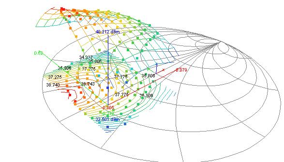
18 Pout (dbm) and Gain (db) Pout (dbm) and Gain (db) Model Validation Large-signal Model validation of a 8x75 µm GaN HEMT with load-pull measurements performed at 6 GHz for optimum PAE load impedance in class-ab Model validation of a 8x400 µm GaN HEMT with load-pull measurements performed at 3 GHz for the optimum Pout load impedance in class-b meas. model Pout PAE gain PAE (%) meas. model Pout gain PAE PAE (%) Pin dbm Pin dbm -20

19 Model Validation VNA Based load pull system is preferred for model validation Specific Architecture DC or pulse DC supplies + meas Units PA Gate T Low loss directional couplers DUT Drain T 50W Tuner f0 VNA Tuner f0, 2f0, 3f0 CW or pulse RF signal f0 or f1+f2
20 Model Validation VNA Based load pull system is preferred for model validation because of the input impedance measurement capability

21 Model Validation Power meter based system are wideband measurement system f0 2.f0 3.f0 VNA based system can be narrowband measurement system f0 f0 f0 2.f0 3.f0 2.f0 3.f0 2.f0 3.f0 More information for model validation or efficient design


22 Model Validation VNA Based load pull system is preferred for model validation Specific Architecture DC or pulse DC supplies + meas Units PA Gate T Low loss directional couplers DUT Drain T 50W Tuner f0 VNA Tuner f0, 2f0, 3f0 CW or pulse RF signal f0 or f1+f2 Phase reference


23 Model Validation Large signal impact - class AB, 25V, 10 GHz Comparison with measurements With non optimal loads : Time domain load pull measurements Deembedding in the intrinsic reference plane Parasitic extrinsic elements must be accurately extracted by previous S parameter measurements
24 Q&A Thank you AMCAD Engineering 20, rue Atlantis Limoges, France Web Site: 24
Nonlinear Characterization and Modeling Through Pulsed IV/S-Parameters
 Nonlinear Characterization and Modeling Through Pulsed IV/S-Parameters OUTLINE Introduction Core device model extraction Model Enhancement Model Validation Types of Large-Signal Transistor Models Convergence
ARFTG - Microwave Measurement Conference. System Modeling and Measurement for High Accuracy Verification
 ARFTG - Microwave Measurement Conference System Modeling and Measurement for High Accuracy Verification December 1st - 4th, 29, Broomfield/Boulder, Colorado OUTLINE PART I : Pulsed IV and S parameters
Méthodes avancées de caractérisation et de modélisation des transistors HEMT GaN
 Méthodes avancées de caractérisation et de modélisation des transistors HEMT GaN Jean Christophe NALLATAMBY, Julien COUVIDAT, Sylvain LAURENT, Raphaël SOMMET, Michel PRIGENT & Raymond QUERE XLIM, CNRS
VNA Based Load Pull Harmonic Measurement De-embedding Dedicated to Waveform Engineering
 VNA Based Load Pull Harmonic Measurement De-embedding Dedicated to Waveform Engineering C. Charbonniaud, T.Gasseling AMCAD ENGINEERING -20 Av Atlantis 87068- LIMOGES - FRANCE Abstract. This paper presents
Nonlinear characterization and modeling of low. power transistors
 Workshop WMB Nonlinear characterization and modeling of low frequency dispersive effects in power transistors R. Quéré (1), O. Jardel (2), A. Xiong (1), M. Oualli (2), T. Reveyrand (1), J.P. Teyssier (1),
TGF Watt Discrete Power GaN on SiC HEMT. Key Features. Measured Performance. Primary Applications Space Military Broadband Wireless
 12 Watt Discrete Power GaN on SiC HEMT Key Features Frequency Range: DC - 18 GHz > 41 dbm Nominal Psat 55% Maximum PAE 15 db Nominal Power Gain Bias: Vd = 28-40 V, Idq = 250 ma, Vg = -3 V Typical Technology:
TGF Watt Discrete Power GaN on SiC HEMT. Key Features. Measured Performance. Primary Applications Space Military Broadband Wireless
 6 Watt Discrete Power GaN on SiC HEMT Key Features Frequency Range: DC - 18 GHz > 38 dbm Nominal Psat 55% Maximum PAE 15 db Nominal Power Gain Bias: Vd = 28-40 V, Idq = 125 ma, Vg = -3 V Typical Technology:
Spurious and Stability Analysis under Large-Signal Conditions using your Vector Network Analyser
 Spurious and Stability Analysis under Large-Signal Conditions using your Vector Network Analyser An application of ICE June 2012 Outline Why combining Large-Signal and Small-Signal Measurements Block Diagram
TGF Watt Discrete Power GaN on SiC HEMT. Key Features. Primary Applications Defense & Aerospace Broadband Wireless. Product Description
 50 Watt Discrete Power GaN on SiC HEMT Key Features Frequency Range: DC - 18 GHz 47 dbm Nominal Psat 55% Maximum PAE 8.7 db Nominal Power Gain Bias: Vd = 28-35 V, Idq = 1 A, Vg = -3.6 V Typical Technology:
Load Pull Validation of Large Signal Cree GaN Field Effect Transistor (FET) Model
 Model") APPLICATION NOTE Load Pull Validation of Large Signal Cree GaN Field Effect Transistor (FET) Model Introduction Large signal models for RF power transistors, if matched well with measured performance,
APPLICATION NOTE Load Pull Validation of Large Signal Cree GaN Field Effect Transistor (FET) Model Introduction Large signal models for RF power transistors, if matched well with measured performance,
DC - 20 GHz Discrete power phemt
 DC - 20 GHz Discrete power phemt Product Description The TriQuint is a discrete 0.6 mm phemt which operates from DC-20 GHz. The is designed using TriQuint s proven standard 0.3um power phemt production
Completing the Design Flow. A Short Course Covering Component-Level Modeling and Measurement, Circuit Design and Analysis and System Modeling
 Completing the Design Flow A Short Course Covering Component-Level Modeling and Measurement, Circuit Design and Analysis and System Modeling Demystifying Device Characterization Abstract - Device characterization
Completing the Design Flow
 Completing the Design Flow A Short Course Covering Component-Level Modeling and Measurement, Circuit Design and Analysis and System Modeling Demystifying Device Characterization Abstract - Device characterization
A new nonlinear HEMT model allowing accurate simulation of very low IM 3 levels for high-frequency highly linear amplifiers design
 A new nonlinear HEMT model allowing accurate simulation of very low IM 3 levels for high-frequency highly linear amplifiers design J. Lhortolary 1, C. Chang 1, T. Reveyrand 2, M. Camiade 1, M. Campovecchio
X-Parameters with Active and Hybrid Active Load Pull
 X-Parameters with Active and Hybrid Active Load Pull Gary Simpson, CTO Maury Microwave EuMW 2012 www.maurymw.com 1 General Load Pull Overview 2 Outline 1. Introduction to Maury Microwave 2. Basics and
IVCAD Advanced Measurement & Modeling Software
 IVCAD Advanced Measurement & Modeling Software DATA SHEET / 4T-022 IVCAD SOFTWARE SUITE MODULES: MT930B1 IVCAD Basic Visualization MT930B2 IVCAD Advanced Visualization Add-On MT930C IVCAD Vector-Receiver
Integrated, Turnkey Modeling and Measurement Systems
 Integrated, Turnkey Modeling and Measurement Systems Cover Feature Invited Papers From Keysight Technologies National Instruments Maury Microwave Focus Microwaves Editor s Note: As time-to-market demands
Low Noise Amplifier Design
 THE UNIVERSITY OF TEXAS AT DALLAS DEPARTMENT OF ELECTRICAL ENGINEERING EERF 6330 RF Integrated Circuit Design (Spring 2016) Final Project Report on Low Noise Amplifier Design Submitted To: Dr. Kenneth
The Design of A 125W L-Band GaN Power Amplifier
 Sheet Code RFi0613 White Paper The Design of A 125W L-Band GaN Power Amplifier This paper describes the design and evaluation of a single stage 125W L-Band GaN Power Amplifier using a low-cost packaged
Next Generation Curve Tracing & Measurement Tips for Power Device. Kim Jeong Tae RF/uW Application Engineer Keysight Technologies
 Next Generation Curve Tracing & Measurement Tips for Power Device Kim Jeong Tae RF/uW Application Engineer Keysight Technologies Agenda Page 2 Conventional Analog Curve Tracer & Measurement Challenges
1W High Linearity and High Efficiency GaAs Power FETs
 1W High Linearity and High Efficiency GaAs Power FETs FEATURES! 1W Typical Power at 6 GHz PHOTO ENLARGEMENT! Linear Power Gain: G L = 13 db Typical at 6 GHz! High Linearity: IP3 = 4 dbm Typical at 6 GHz!
Tour Agilent ADS EMPro 2011 Stability Analysis of Microwave Circuits
 Tour Agilent ADS EMPro 2011 Stability Analysis of Microwave Circuits S. Dellier, PhD AMCAD Engineering Introduction to AMCAD s products and services AMCAD is a provider of new RF & Microwave solutions
High Power Wideband AlGaN/GaN HEMT Feedback. Amplifier Module with Drain and Feedback Loop. Inductances
 High Power Wideband AlGaN/GaN HEMT Feedback Amplifier Module with Drain and Feedback Loop Inductances Y. Chung, S. Cai, W. Lee, Y. Lin, C. P. Wen, Fellow, IEEE, K. L. Wang, Fellow, IEEE, and T. Itoh, Fellow,
40W Power Packaged Transistor. GaN HEMT on SiC
 Gain (db), Pout (dbm) & PAE (%) Id (A) Description 40W Power Packaged Transistor The is an unmatched packaged Gallium Nitride High Electron Mobility Transistor. It offers general purpose and broadband
25W Power Packaged Transistor. GaN HEMT on SiC
 25W Power Packaged Transistor GaN HEMT on SiC Description The is an unmatched packaged Gallium Nitride High Electron Mobility Transistor. It offers general purpose and broadband solutions for a variety
MECXQMM-60W. 8.3 to 10.3 GHz GaN HEMT Power Amplifier
 Pout (dbm), PAE(%) Functional Block Diagram Main Features 0.25µm GaN HEMT Technology 8.3 10.3 GHz full performances Frequency Range 60W Output Power @ Pin 40.5 dbm PAE > 33% @ Pin 40.5 dbm Linear Gain
Development of Gallium Nitride High Electron Mobility Transistors for Cellular Base Stations
 ELECTRONICS Development of Gallium Nitride High Electron Mobility Transistors for Cellular Base Stations Kazutaka INOUE*, Seigo SANO, Yasunori TATENO, Fumikazu YAMAKI, Kaname EBIHARA, Norihiko UI, Akihiro
Introduction to Measurements for Power Transistor Characterization
 Jan Verspecht bvba Mechelstraat 17 B-1745 Opwijk Belgium email: contact@janverspecht.com web: http://www.janverspecht.com Introduction to Measurements for Power Transistor Characterization Fabien De Groote,
PART I - DOUBLE- PULSE GAN FET NONLINEAR CHARACTERIZATION AND MODELING
 Nonlinear Characteriza/on and Modelling of Microwave Electron Devices for Large Signal and Low Noise Applica/ons PART I - DOUBLE- PULSE GAN FET NONLINEAR CHARACTERIZATION AND MODELING Prof. Alberto Santarelli
85W Power Transistor. GaN HEMT on SiC
 GaN HEMT on SiC Description The is a 85W Gallium Nitride High Electron Mobility Transistor. This product offers a general purpose and broadband solution for a variety of RF power applications such as radar
Using Large-Signal Measurements for Transistor Characterization and Model Verification in a Device Modeling Program
 Using Large-Signal Measurements for Transistor Characterization and Model Verification in a Device Modeling Program Maciej Myśliński1, Giovanni Crupi2, Marc Vanden Bossche3, Dominique Schreurs1, and Bart
& ) > 35W, 33-37% PAE
 > 35W, 33-37% PAE") Outline Status of Linear and Nonlinear Modeling for GaN MMICs Presented at IMS11 June, 11 Walter R. Curtice, Ph. D. Consulting www.curtice.org State of the Art Modeling considerations, types of models,
Outline Status of Linear and Nonlinear Modeling for GaN MMICs Presented at IMS11 June, 11 Walter R. Curtice, Ph. D. Consulting www.curtice.org State of the Art Modeling considerations, types of models,
1KV PIV. High Voltage Pulsed IV measurements. Inovative Test System AMCAD ENGINEERING. June 2013
 1KV PIV Inovative Test System High Voltage Pulsed IV measurements AMCAD ENGINEERING June 2013 1 Agenda 1KV PIV Overview Pulsed IV measurement concept Main Specifications Integration with instruments Measurement
MECGaNC30. 4 to 6 GHz GaN HEMT Power Amplifier. Main Features. Product Description. Applications
 Main Features 0.25µm GaN HEMT Technology 4.1 5.9 GHz full performances Frequency Range W Output Power @ Pin 27.5 dbm 37% PAE @ Pin 27.5 dbm % PAE @ Pout Watt 27 db Small Signal Gain Product Description
Very small duty cycles for pulsed time domain transistor characterization
 EUROPEAN MICROWAVE ASSOCIATION Very small duty cycles for pulsed time domain transistor characterization Fabien De Groote 1, Olivier Jardel 2, Tibault Reveyrand 2, Jean-Pierre Teyssier 1, 2 and Raymond
Small Signal Modelling of InGaAs/InAlAs phemt for low noise applications
 Small Signal Modelling of InGaAs/InAlAs phemt for low noise applications N. Ahmad and M. Mohamad Isa School of Microelectronic Engineering, Universiti Malaysia Perlis, Pauh Putra Campus, 26 Arau, Perlis,
LOW NOISE L TO K-BAND GaAs MESFET SYMBOLS PARAMETERS AND CONDITIONS UNITS MIN TYP MAX NFOPT 1
 FEATURES LOW NOISE FIGURE NF = 1.6 db TYP at f = 1 GHz HIGH ASSOCIATED GAIN GA = 9.5 db TYP at f = 1 GHz LG = 0.3 µm, WG = 80 µm EPITAXIAL TECHNOLOGY LOW PHASE NOISE DESCRIPTION The features a low noise
ANALYSIS OF BROADBAND GAN SWITCH MODE CLASS-E POWER AMPLIFIER
 Progress In Electromagnetics Research Letters, Vol. 38, 151 16, 213 ANALYSIS OF BROADBAND GAN SWITCH MODE CLASS-E POWER AMPLIFIER Ahmed Tanany, Ahmed Sayed *, and Georg Boeck Berlin Institute of Technology,
Adaptive Second Harmonic Active Load For Pulsed-IV/RF Class-B Operation
 Adaptive Second Harmonic Active Load For Pulsed-IV/RF Class-B Operation Seok Joo Doo, Patrick Roblin, Venkatesh Balasubramanian, Richard Taylor, Krishnanshu Dandu, Gregg H. Jessen, and Roberto Rojas Electrical
High Frequency Small-Signal Modelling of GaN High Electron Mobility Transistors for RF applications
 High Frequency Small-Signal Modelling of GaN High Electron Mobility Transistors for RF applications by Zhen Liu B.ENG., University of Electronic Science and Technology of China, 2013 A Project Report Submitted
EC2612 RoHS COMPLIANT
 40GHz Super Low Noise PHEMT Pseudomorphic High Electron Mobility Transistor EC2612 RoHS COMPLIANT Description The EC2612 is based on a 0.15µm gate pseudomorphic high electron mobility transistor (0.15µm
Design of Class F Power Amplifiers Using Cree GaN HEMTs and Microwave Office Software to Optimize Gain, Efficiency, and Stability
 White Paper Design of Class F Power Amplifiers Using Cree GaN HEMTs and Microwave Office Software to Optimize Gain, Efficiency, and Stability Overview This white paper explores the design of power amplifiers
15W Power Packaged Transistor. GaN HEMT on SiC
 Gain (db), Pout (dbm) & PAE (%) Drain Current (A) CHK15A-QIA Description The CHK15A-QIA is an unmatched packaged Gallium Nitride High Electron Mobility Transistor. It offers general purpose and broadband
Agilent Technologies Gli analizzatori di reti della serie-x
 Agilent Technologies Gli analizzatori di reti della serie-x Luigi Fratini 1 Introducing the PNA-X Performance Network Analyzer For Active Device Test 500 GHz & beyond! 325 GHz 110 GHz 67 GHz 50 GHz 43.5
DESIGN OF AN ULTRA-EFFICIENT GAN HIGH POWER AMPLIFIER FOR RADAR FRONT-ENDS USING ACTIVE HARMONIC LOAD-PULL
 DESIGN OF AN ULTRA-EFFICIENT GAN HIGH POWER AMPLIFIER FOR RADAR FRONT-ENDS USING ACTIVE HARMONIC LOAD-PULL Tushar Thrivikraman, James Hoffman Jet Propulsion Laboratory, California Institute of Technology
An Asymmetrical Bulk CMOS Switch for 2.4 GHz Application
 Progress In Electromagnetics Research Letters, Vol. 66, 99 104, 2017 An Asymmetrical Bulk CMOS Switch for 2.4 GHz Application Lang Chen 1, * and Ye-Bing Gan 1, 2 Abstract A novel asymmetrical single-pole
AU4850 Pulsed IV/RF Characterization System
 FOURTH GENERATION PULSED IV/RF Featuring 220 V, 30 A with 0.01% Current Resolution for RF designers S-parameter Option for Major Network Analyzers Pulsed Load-pull Option 1200 V, 30 A with Enhanced ON-resistance
Large-Signal Network Analysis Technology for HF analogue and fast switching components
 Large-Signal Network Analysis Technology for HF analogue and fast switching components Applications This slide set introduces the large-signal network analysis technology applied to high-frequency components.
A Testbench for Analysis of Bias Network Effects in an RF Power Amplifier with DPD. Marius Ubostad and Morten Olavsbråten
 A Testbench for Analysis of Bias Network Effects in an RF Power Amplifier with DPD Marius Ubostad and Morten Olavsbråten Dept. of Electronics and Telecommunications Norwegian University of Science and
Simulations of High Linearity and High Efficiency of Class B Power Amplifiers in GaN HEMT Technology
 Simulations of High Linearity and High Efficiency of Class B Power Amplifiers in GaN HEMT Technology Vamsi Paidi, Shouxuan Xie, Robert Coffie, Umesh K Mishra, Stephen Long, M J W Rodwell Department of
ARFTG Workshop, Boulder, December 2014
 ARFTG Workshop, Boulder, December 2014 Design and measurements of high-efficiency PAs with high PAR signals Zoya Popovic, Tibault Reveyrand, David Sardin, Mike Litchfield, Scott Schafer, Andrew Zai Department
10 W, GaN Power Amplifier, 2.7 GHz to 3.8 GHz HMC1114
 9 13 16 FEATURES High saturated output power (PSAT): 41.5 dbm typical High small signal gain: db typical High power gain for saturated output power:.5 db typical Bandwidth: 2.7 GHz to 3.8 GHz High power
Wideband Reconfigurable Harmonically Tuned GaN SSPA for Cognitive Radios
 The University Of Cincinnati College of Engineering Wideband Reconfigurable Harmonically Tuned GaN SSPA for Cognitive Radios Seth W. Waldstein The University of Cincinnati-Main Campus Miguel A. Barbosa
GaN HEMT SPICE Model Standard for Power & RF. Samuel Mertens MOS-AK Workshop Washington, DC December 9, 2015
 GaN HEMT SPICE Model Standard for Power & RF Samuel Mertens MOS-AK Workshop Washington, DC December 9, 2015 Compact Model Coalition @SI2 Standardizing Compact Models Since 1996 Started with BSIM3 Support
New LDMOS Model Delivers Powerful Transistor Library Part 1: The CMC Model
 From October 2004 High Frequency Electronics Copyright 2004, Summit Technical Media, LLC New LDMOS Model Delivers Powerful Transistor Library Part 1: The CMC Model W. Curtice, W.R. Curtice Consulting;
Fnl(VGo,VDo,Vg,Vd,W) Fnl(VGo,VDo,Vg,Vd,W,T)
 Fnl(VGo,VDo,Vg,Vd,W,T)") What about Temperature What about Temperature Static Dynamic Geometry Self Heating L.F. Dispersion Channel Geometry Scaling Rules Fnl(VGo,VDo,Vg,Vd,W) Large Signal Static & Dynamic EXTERNAL & INTERNAL
What about Temperature What about Temperature Static Dynamic Geometry Self Heating L.F. Dispersion Channel Geometry Scaling Rules Fnl(VGo,VDo,Vg,Vd,W) Large Signal Static & Dynamic EXTERNAL & INTERNAL
Measurements for Optimization of Solid-State Power Amplifiers
 Session 3: Characterization and modeling Measurements for Optimization of Solid-State Power Amplifiers Jean-Pierre Teyssier, Tibault Reveyrand, Denis Barataud XLIM C²S², University of Limoges, 127 avenue
IRFE230 JANTXV2N6798U SURFACE MOUNT (LCC-18) 200V, N-CHANNEL REF:MIL-PRF-19500/557. Absolute Maximum Ratings PD-91715C.
 200V, N-CHANNEL REF:MIL-PRF-19500/557. Absolute Maximum Ratings PD-91715C.") PD-975C REPETITIVE AVALANCHE AND dv/dt RATED HEXFET TRANSISTORS SURFACE MOUNT (LCC-8) Product Summary Part Number BVDSS RDS(on) ID IRFE230 200V 0.40Ω 5.5A IRFE230 JANTX2N6798U JANTXV2N6798U REF:MIL-PRF-9500/557
PD-975C REPETITIVE AVALANCHE AND dv/dt RATED HEXFET TRANSISTORS SURFACE MOUNT (LCC-8) Product Summary Part Number BVDSS RDS(on) ID IRFE230 200V 0.40Ω 5.5A IRFE230 JANTX2N6798U JANTXV2N6798U REF:MIL-PRF-9500/557
Recent Advances in the Measurement and Modeling of High-Frequency Components
 Jan Verspecht bvba Gertrudeveld 15 184 Steenhuffel Belgium email: contact@janverspecht.com web: http://www.janverspecht.com Recent Advances in the Measurement and Modeling of High-Frequency Components
NEC'S 3W, L/S-BAND MEDIUM POWER GaAs MESFET PACKAGE OUTLINE
 FEATURES NEC'S 3W, L/S-BAND MEDIUM POWER GaAs MESFET LOW COST PLASTIC SURFACE MOUNT PACKAGE Available on Tape and Reel USABLE TO.7 GHz: Fixed Wireless Access, ISM, WLL, MMDS, IMT-, PCS HIGH OUTPUT POWER:
Preliminary Datasheet Revision: January 2016
 Preliminary Datasheet Revision: January 216 Applications Point-to-Point Digital Radios Point-to-Multipoint Digital Radios SATCOM Terminals X = 3.65mm Y = 2.3mm Product Features RF frequency: 27 to 31 GHz
CHAPTER 4 ULTRA WIDE BAND LOW NOISE AMPLIFIER DESIGN
 93 CHAPTER 4 ULTRA WIDE BAND LOW NOISE AMPLIFIER DESIGN 4.1 INTRODUCTION Ultra Wide Band (UWB) system is capable of transmitting data over a wide spectrum of frequency bands with low power and high data
5W X Band Medium Power Amplifier. GaN Monolithic Microwave IC
 GaN Monolithic Microwave IC Description V+ The CHA6710-99F is a two stage Medium Power Amplifier operating between 8.0 and 12.75GHz. It typically provides 5W of saturated output power and 36% of power
60-W, GHz Push-Pull Amplifier for IMT-2000 Base Station Application using the FLL600IQ-2C GaAs FET
 60-W, 2.11 2.17 GHz Push-Pull Amplifier for IMT-2000 Base Station Application using the FLL600IQ-2C GaAs FET FEATURES Targeted WCDMA ACPR at 6 W Average Over 60 Watts P out over entire band High gain Easy
IRHG V, Quad N-CHANNEL RADIATION HARDENED POWER MOSFET THRU-HOLE (MO-036) PD-94432C. 1 TECHNOLOGY. Product Summary MO-036AB
 PD-94432C. 1 TECHNOLOGY. Product Summary MO-036AB") PD-94432C RADIATION HARDENED POWER MOSFET THRU-HOLE (MO-36) Product Summary Part Number Radiation Level RDS(on) ID IRHG57 K Rads (Si).29Ω.6A IRHG53 3K Rads (Si).29Ω.6A IRHG54 5K Rads (Si).29Ω.6A IRHG58
PD-94432C RADIATION HARDENED POWER MOSFET THRU-HOLE (MO-36) Product Summary Part Number Radiation Level RDS(on) ID IRHG57 K Rads (Si).29Ω.6A IRHG53 3K Rads (Si).29Ω.6A IRHG54 5K Rads (Si).29Ω.6A IRHG58
MT1000 and MT2000 Mixed-Signal Active Load Pull System (1.0 MHz to 40.0 GHz) And MT2001 System Software
 And MT2001 System Software") MT1000 and MT0 Mixed-Signal Active Load Pull System (1.0 MHz to 40.0 GHz) And MT1 System Software DATA SHEET / 4T-097 U.S. Patent No. 8,456,175 B2 Several international patents also available // SEPTEMBER
MT1000 and MT0 Mixed-Signal Active Load Pull System (1.0 MHz to 40.0 GHz) And MT1 System Software DATA SHEET / 4T-097 U.S. Patent No. 8,456,175 B2 Several international patents also available // SEPTEMBER
18W X-Band High Power Amplifier. GaN Monolithic Microwave IC
 CHA8611-99F GaN Monolithic Microwave IC Description V+ The CHA8611-99F is a two stage High Power Amplifier operating between 8.5 and 11GHz and providing typically 18W of saturated output power and 43%
Rating Symbol Value Unit Drain Source Voltage VDSS 65 Vdc Drain Gate Voltage (RGS = 1.0 MΩ)
") SEMICONDUCTOR TECHNICAL DATA Order this document by MRF275G/D The RF MOSFET Line N Channel Enhancement Mode Designed primarily for wideband large signal output and driver stages from 1 5 MHz. Guaranteed
SEMICONDUCTOR TECHNICAL DATA Order this document by MRF275G/D The RF MOSFET Line N Channel Enhancement Mode Designed primarily for wideband large signal output and driver stages from 1 5 MHz. Guaranteed
InAlN/GaN HEMTs Technologies for Microwave, Fast switching and Mixed Signal Applications
 InAlN/GaN HEMTs Technologies for Microwave, Fast switching and Mixed Signal Applications S.DELAGE / S.PIOTROWICZ Summary III-V Lab presentation Motivations Technology for L & S band applications Technology
High Efficiency Classes of RF Amplifiers
 Rok / Year: Svazek / Volume: Číslo / Number: Jazyk / Language 2018 20 1 EN High Efficiency Classes of RF Amplifiers - Erik Herceg, Tomáš Urbanec urbanec@feec.vutbr.cz, herceg@feec.vutbr.cz Faculty of Electrical
IVCAD VNA Base Load Pull with Active/Hybrid Tuning. Getting Started v3.5
 IVCAD VNA Base Load Pull with Active/Hybrid Tuning Getting Started v3.5 1 Setting and Configuration Block Diagram... 3 1.1 VNA setup... 5 1.2 RF source setup... 6 1.3 Power meter setup... 7 1.4 Source
GaN/SiC Bare Die Power HEMT DC-15 GHz
 GaN/SiC Bare Die Power HEMT DC-15 GHz DESCRIPTION AMCOM s is a discrete GaN/SiC HEMT that has a total gate width of mm (Eight 1.mm FETs in parallel). It is a bare die which can be operated up to 15 GHz.
Characterization and Modeling of LDMOS Power FETs for RF Power Amplifier Applications
 Characterization and ing of LDMOS Power FETs for RF Power Amplifier Applications (Invited Paper) John Wood, Peter H. Aaen, and Jaime A. Plá Freescale Semiconductor Inc., RF Division 2100 E. Elliot Rd.,
100nm GaN on Si: A Pioneering Technology to Enable High RF Power in Millimeter Wave Bands NEW ENGLAND IMAPS SYMPOSIUM MAY 5, 2015
 Innovating with III-V s 100nm GaN on Si: A Pioneering Technology to Enable High RF Power in Millimeter Wave Bands NEW ENGLAND IMAPS SYMPOSIUM MAY 5, 2015 By Dr Fabien ROBERT Sales & Application Team Manager,
GaN-HEMT VSWR Ruggedness and Amplifier Protection
 GaN-HEMT VSWR Ruggedness and Amplifier Protection Microwave Technology and Techniques Workshop 2010 10-12 May 2010 ESA-ESTEC, Noordwijk, The Netherlands O. Bengtsson (1), G. van der Bent (2), M. Rudolph
T1G FS 30W, 28V, DC 6 GHz, GaN RF Power Transistor
 Applications Military radar Civilian radar Professional and military radio communications Test instrumentation Wideband or narrowband amplifiers Jammers Product Features Frequency: DC to 6 GHz Output Power
transistor is available in a flange and pill package. Package Types: & PN s: CGH40045F & CGH40045P
 Rev 4.0 - May 2015 CGH40045 45 W, DC - 4 GHz RF Power GaN HEMT Cree s CGH40045 is an unmatched, gallium nitride (GaN) high electron mobility transistor (HEMT). The CGH40045, operating from a 28 volt rail,
Power Amplifier Design Utilizing the NVNA and X-parameters
 IMS2011 Power Amplifier Design Utilizing the NVNA and X-parameters Loren Betts 1, Dylan T. Bespalko 2, Slim Boumaiza 2 1 Agilent Technologies, Santa Rosa CA, USA 2 University of Waterloo, Waterloo ON,
Advance Datasheet Revision: April 2015
 APN 1-1 GHz Advance Datasheet Revision: April Applications Point-to-Point Digital Radios Point-to-Multipoint Digital Radios VSAT Test Instrumentation X = 3 um Y = 3 um Product Features RF frequency: 1
How to Design Power Electronics
 How to Design Power Electronics The HF in Power Semiconductor Modeling and Design September 3, 2015 Ingmar Kallfass Institute of Robust Power Semiconductor Systems University of Stuttgart Outline Semiconductor-Based
Gallium Nitride MMIC Power Amplifier
 Gallium Nitride MMIC Power Amplifier August 2015 Rev 4 DESCRIPTION AMCOM s is an ultra-broadband GaN MMIC power amplifier. It has 21dB gain, and >41dBm output power over the 0.03 to 6GHz band. This MMIC
High-Efficiency L-Band 200-W GaN HEMT for Space Applications
 INFOCOMMUNICATIONS High-Efficiency L-Band 200-W GaN HEMT for Space Applications Ken OSAWA*, Hiroyuki YOSHIKOSHI, Atsushi NITTA, Tsuneyuki TANAKA, Eizo MITANI, and Tomio SATOH ----------------------------------------------------------------------------------------------------------------------------------------------------------------------------------------------------------------------------------------------------------
Microwave Technology
 GUC (Dr. Hany Hammad) 9/5/06 Microwave Technology (COMM 903) Contents Introduction: Course contents. Assessment. eferences. Microwave Sources. Transistor Model Extraction. Signal flow graphs. COMM (903)
GaN/SiC Bare Die Power HEMT DC-15 GHz
 GaN/SiC Bare Die Power HEMT DC-15 GHz DESCRIPTION AMCOM s is a discrete GaN/SiC HEMT that has a total gate width of 5mm (Four 1.mm FETs in parallel). It is a bare die which can be operated up to 15 GHz.
A 2.4GHz Fully Integrated CMOS Power Amplifier Using Capacitive Cross-Coupling
 A 2.4GHz Fully Integrated CMOS Power Amplifier Using Capacitive Cross-Coupling JeeYoung Hong, Daisuke Imanishi, Kenichi Okada, and Akira Tokyo Institute of Technology, Japan Contents 1 Introduction PA
Part Number: IGN2735M250
 S-Band Radar Transistor IGN2735M250 is an internally pre-matched, gallium nitride (GaN) high electron mobility transistor (HEMT). This part is designed for S-Band radar applications operating over the
IRHF57034 THRU-HOLE (TO-39) REF: MIL-PRF-19500/701. Absolute Maximum Ratings PD-93791D
 REF: MIL-PRF-19500/701. Absolute Maximum Ratings PD-93791D") PD-9379D RADIATION HARDENED POWER MOSFET THRU-HOLE (TO-39) Product Summary Part Number Radiation Level RDS(on) ID QPL Part Number IRHF5734 K Rads (Si).48Ω 2A* JANSR2N7492T2 IRHF5334 3K Rads (Si).48Ω 2A*
PD-9379D RADIATION HARDENED POWER MOSFET THRU-HOLE (TO-39) Product Summary Part Number Radiation Level RDS(on) ID QPL Part Number IRHF5734 K Rads (Si).48Ω 2A* JANSR2N7492T2 IRHF5334 3K Rads (Si).48Ω 2A*
Capacitive-Division Traveling-Wave Amplifier with 340 GHz Gain-Bandwidth Product
 Hughes Presented at the 1995 IEEE MTT-S Symposium UCSB Capacitive-Division Traveling-Wave Amplifier with 340 GHz Gain-Bandwidth Product J. Pusl 1,2, B. Agarwal1, R. Pullela1, L. D. Nguyen 3, M. V. Le 3,
CHA F RoHS COMPLIANT
 Pout (dbm) & PAE(%) & Gain(dB) RoHS COMPLIANT GaAs Monolithic Microwave IC Description The is a monolithic two-stage GaAs medium power amplifier designed for X-band applications. The MPA provides typically
>10 W, GaN Power Amplifier, 0.01 GHz to 1.1 GHz HMC1099
 9 1 11 12 13 14 1 16 32 GND 31 29 28 27 26 FEATURES High saturated output power (PSAT):. dbm typical High small signal gain: 18. db typical High power added efficiency (PAE): 69% typical Instantaneous
Keysight Technologies Nonlinear Vector Network Analyzer (NVNA) Breakthrough technology for nonlinear vector network analysis from 10 MHz to 67 GHz
 Breakthrough technology for nonlinear vector network analysis from 10 MHz to 67 GHz") Keysight Technologies Nonlinear Vector Network Analyzer (NVNA) Breakthrough technology for nonlinear vector network analysis from 1 MHz to 67 GHz 2 Keysight Nonlinear Vector Network Analyzer (NVNA) - Brochure
Keysight Technologies Nonlinear Vector Network Analyzer (NVNA) Breakthrough technology for nonlinear vector network analysis from 1 MHz to 67 GHz 2 Keysight Nonlinear Vector Network Analyzer (NVNA) - Brochure
New Wide Band Gap High-Power Semiconductor Measurement Techniques Accelerate your emerging material device development
 New Wide Band Gap High-Power Semiconductor Measurement Techniques Accelerate your emerging material device development Alan Wadsworth Americas Market Development Manager Semiconductor Test Division July
drain supply terminal impedance at signal envelope frequencies
 WSM: Characterization of transistor drain supply terminal impedance at signal envelope frequencies Zoya Popovic, Scott Schafer, David Sardin, Tibault Reveyrand * University it of Colorado, Boulder *XLIM,
RF IV Waveform Measurement and Engineering
 RF IV Waveform Measurement and Engineering - Emerging Multi-Tone Systems - Centre for High Frequency Engineering School of Engineering Cardiff University Contact information Prof. Paul J Tasker tasker@cf.ac.uk
Advance Datasheet Revision: May 2013
 Applications Military SatCom Phased-Array Radar Applications Point-to-Point Radio Point-to-Multipoint Communications Terminal Amplifiers X = 4.4mm Y = 2.28mm Product Features RF frequency: 18 to 23 GHz
Large-signal PHEMT and HBT modeling for power amplifier applications. Ce-Jun Wei Skyworks Inc. Sept
 Large-signal PHEMT and HBT modeling for power amplifier applications Ce-Jun Wei Skyworks Inc. Sept. 9 2002 Agenda Introduction Phemt modeling issues Empirical model vs table-based model; Charge model vs
T2G Q3 10W, 28V DC 6 GHz, GaN RF Power Transistor
 Applications Military radar Civilian radar Professional and military radio communications Test instrumentation Wideband or narrowband amplifiers Jammers Product Features Frequency: DC to 6 GHz Output Power
Fig. 1 - Enhancement mode GaN has a circuiut schematic similar to silicon MOSFETs with Gate (G), Drain (D), and Source (S).
, Drain (D), and Source (S).") GaN Basics: FAQs Sam Davis; Power Electronics Wed, 2013-10-02 Gallium nitride transistors have emerged as a high-performance alternative to silicon-based transistors, thanks to the technology's ability
GaN Basics: FAQs Sam Davis; Power Electronics Wed, 2013-10-02 Gallium nitride transistors have emerged as a high-performance alternative to silicon-based transistors, thanks to the technology's ability
RF W GaN WIDEBAND PULSED POWER AMPLIFIER
 280W GaN WIDE- BAND PULSED POWER AMPLI- FIER 280W GaN WIDEBAND PULSED POWER AMPLIFIER Package: Hermetic 2-Pin, Flanged Ceramic Features Wideband Operation 2.8GHz to 3.4GHz Advanced GaN HEMT Technology
Large-Signal Measurements Going beyond S-parameters
 Large-Signal Measurements Going beyond S-parameters Jan Verspecht, Frans Verbeyst & Marc Vanden Bossche Network Measurement and Description Group Innovating the HP Way Overview What is Large-Signal Network