Design of Class F Power Amplifiers Using Cree GaN HEMTs and Microwave Office Software to Optimize Gain, Efficiency, and Stability
|
|
|
- Millicent Garrison
- 5 years ago
- Views:
Transcription
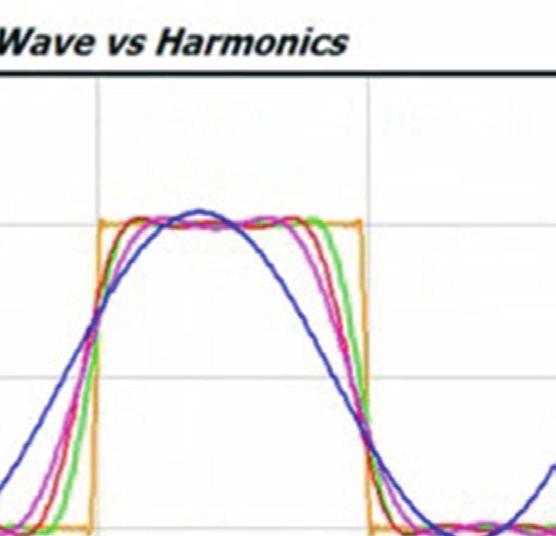
1 White Paper Design of Class F Power Amplifiers Using Cree GaN HEMTs and Microwave Office Software to Optimize Gain, Efficiency, and Stability Overview This white paper explores the design of power amplifiers employing Cree GaN HEMTs to maximize power-added efficiency (PAE) by optimizing source and load pull at both fundamental and harmonic frequencies. The load-pull scripts that are available in Microwave Office circuit design software have been used extensively to find the optimum trade-offs in power gain, efficiency, and stability. The paper will specifically describe the basis of Class F PA and inverse Class F design F, as well as a relatively new approach called continuous Class F, which enables greater bandwidths to be realized. Design examples are given, including the inspection of voltage and current waveforms for both packaged and bare die transistors in the 10 to 25 watt power range for frequencies up to 2.5 GHz. Achieving High Efficiency The highest efficiency power amplifiers use switch-mode operation Classes D, E, F and others. Earlier modes of amplification (Classes A, B and C) are defined by the conduction angle established by the bias point, and are driven with sine wave signals. Switch-mode PAs are all biased at the turn-on threshold and driven either with square wave signals or with sine waves with sufficient amplitude to switch the power device almost as quickly as true square waves. The output of an ideal switched power device is also a square wave, which contains significant energy at harmonics of the fundamental frequency. The various classes of switch-mode amplification are defined by the way the output network deals with the harmonics, e.g., whether they are terminated with an open or short circuit. The operation of each class corresponds to a particular voltage and current waveform at the output terminal of the power device. Finally, these PAs are used with advanced linearization techniques such as envelope tracking, outphasing and digital predistortion, and must have reliable, repeatable designs that require minimum adjustment on the assembly line and have stable performance in the field over their operational lifetime. Simulation tools are an essential part of the design process for switch-mode PAs. To achieve maximum performance, the designer must have tools that support design and optimization to obtain the desired voltage and current waveforms. Circuit simulation, thermal analysis and board layout for RF and DC must all be done in concert, with accurate results. Design shortfalls must be identified and quickly resolved in simulation, before any hardware is constructed competition and rapidly changing technology simply do not allow multiple prototype iterations. The simulation platform must include robust mathematics, highly accurate device and circuit element models, and must have operational features that support an engineer s design effort in the same manner as the best prototype shop and test bench. ni.com/awr
2

3 Inverse Class F, as the name implies, has opposite voltage and current waveforms. The same schematic also represent this class if the waveforms were reversed, e.g., a half sine voltage waveform and square current waveform. The way harmonics are handled is also reversed. For the same Cree GaN HEMT in an Inverse Class F mode of operation, the input-matching network is basically the same and the output network still has the series-tuned resonator, but the quarter wave transmission line is moved from the shunt bias line to the RF output line, where it again is used to manage the harmonics. Waverforms obtained for this instance reveal a square wave for current and a half sine wave for voltage waveform. The drain current measurement swings below zero due to circuit parasitic effects. With this operating condition, the maximum efficiency of the PA reaches 87 percent. Fundamental and Harmonic Load Pull using Microwave Office Load Pull Wizard To take the next step in design, engineers can use a powerful feature in Microwave Office, the Load Pull Wizard. The PA designer must simultaneously find the most efficient impedance match at the fundamental while properly terminating each harmonic with the necessary short or open circuit. It would be extremely time consuming to run a series of laboratory load pull tests to determine the impedances at fundamental and harmonic frequencies which will result in the proper I and V waveforms. The ability to use load pull simulation to determine these impedances greatly speeds and simplifies the design process. The first task is to do determine input matching with a source pull for power gain and power-added efficiency. At this point, the output of the transistor is simply terminated directly into 50 ohms. For output matching, a fundamental frequency load pull is performed, again for power gain and PAE, using the source pull results at the input of the device. Then the second and third harmonic terminations are loaded into the load pull wizard and the load pull tuners set either to arbitrary values or to the values in the basic circuits above for Class F or inverse Class F. Then second and third harmonic source pull and load pull will be invoked with the wizard to find the optimum impedances for best power gain and PAE. When second and third harmonic terminations are included, their impedances may affect the fundamental impedance. Consequently, it will be necessary to iterate the load pull sequence at least twice to get to that optimum point. Transistors and matching networks using practical lumped and distributed components are not perfect, and some waveform engineering will actually be done via the Load Pull Wizard to peak up the efficiency power and gain. Figure 3 shows the basic setup for a series of load pull operations on a basic PA circuit. A source pull tuner is on the left, a load pull tuner is on the right, and bias Ts have been integrated into those tuners as well. The CGH40010F GaN HEMT device is a bare die, so wire bonds are included in the simulation. Figure 3: Microwave Office Load-Pull Wizard within Microwave Office enables simulation instead of costly bench measurements.


4 The first fundamental source pull for gain achieves 15.3 db at the optimum point, which is automatically calculated through all the converged points. The source pull for output power results in a maximum of 43.5 dbm. Finally, the fundamental source pull for power added efficiency, results in an optimum point at an impedance that is very close to the maximum for both gain and power. This simplifies the matching task considerably and even though the load is directly into 50 ohms, the PAE is already over 60 percent at this point. For load pull simulation and optimization, the source pull is set at the impedance that provided the best PAE. The fundamental load pull results for gain, then for power are similar, and fundamental load pull for PAE does not result in a large change. Figure 4 shows the PAE results, which is improved from 60.5 percent with source pull only to 72 percent. At this point both ports are matched for PAE only at the fundamental. With the fundamental source and load pull set to previous values, the wizard can find the optimum second harmonic load pull for maximum PAE. The PAE has improved to over 80 percent. The third harmonic load pull has a smaller effect, providing between one and two percentage points improvement in efficiency. Of course, the design goal for optimum harmonic impedances could also be power gain or output, as needed for the particular application. Now that the required optimum fundamental second and third harmonic terminations have been identified, matching networks can be synthesized to emulate the required impedances as closely as possible over the complete frequency range. This simple case is a relatively narrow band design centered at 2 GHz. Remember that practical networks will approximate, but not exactly match, the impedances that have been defined by the load pull data. Figure 5 is a synthesized Class F input network, which in this case consists of transmission lines, a short-circuited stub on one side and an open-circuited stub on the other. The S11 of this input network at fundamental and harmonics does not exactly match the values determined by the input source pull, since its design is limited to available components and practical distributed elements. Figure 4: PAE after load pull optimization improves from 60.5 percent to 72 percent (both ports matched for PAE at fundamental only) Figure 5: Class F input network obtained by synthesis.

5 The resulting synthesized Class F output network is similar to the one in the basic design circuit. The quarter wave line also provides drain bias to the transistor. In addition there is an open circuit stub that provides a transmission line transformation resulting in an open at the second and a short at the third harmonic. Looking into the input of the network where the drain of the device would be, Figure 6 shows the fundamental, second and third harmonic impedances. Again, going back to the wizard, it can be seen that there are some differences between the practical transmission line-based network and the ideal impedances determined by load pull. The complete circuit with the transistor and bias voltages can be simulated as a whole. Simulation results for power gain, output power, and PAE reveal that the PAE reaches 84 percent, which is slightly better than predicted by the Load Pull Wizard results. As for the waverforms of the drain voltage and current, recall what was noted earlier when source and load pull are done with the Microwave Office wizard, users will get some degree of waveform engineering. If they tell the wizard that they want to have maximum PAE, the wizard s optimization algorithm will try to produce the voltage and current waveforms at the transistor that are not only the right shape but also ideal and anti-phase. It can be seen that the half sine voltage waveform is close to being a half sinusoid, although the current waveform deviates from being square. Again the current goes negative because measurement is not at the intrinsic device terminals. The process of simulating source pull and load pull at the fundamental frequency and harmonics replaces many such tests on the workbench. The Load Pull Wizard has the added value of a final optimization with practical element values obtained by matching network synthesis, with the goal of obtaining the desired voltage and current waveforms. Figure 6: Terminations based on load-pull analysis. The λ/4 shunt transmission line in the drain bias is high Z (open) for odd harmonics, low Z (short) for even harmonics. A Note on Models Subsequent to the work described in this paper being done, Cree has developed a new set of device models with two additional test ports that effectively de-embed device parasitics and allow observation of the drain voltage and current waveforms as if probing directly on the die [8]. Figure 7 below shows a drain waveform using the new model, clearly showing minimal current excursion into the negative region (red trace). Of course, when setting up a simulation the designer must account for parasitics due to transistor mounting and connection to external traces and components. Figure 7: Example of intrinsic (parasitics de-embedded) drain waveforms using the drain voltage and current ports in Cree s new device model.

6
NI AWR Design Environment Load-Pull Simulation Supports the Design of Wideband High-Efficiency Power Amplifiers
 Design NI AWR Design Environment Load-Pull Simulation Supports the Design of Wideband High-Efficiency Power Amplifiers The design of power amplifiers (PAs) for present and future wireless systems requires
A Simulation-Based Flow for Broadband GaN Power Amplifier Design
 Rubriken Application A Simulation-Based Flow for Broadband GaN Power Amplifier Design This application note demonstrates a simulation-based methodology for broadband power amplifier (PA) design using load-line,
Leveraging High-Accuracy Models to Achieve First Pass Success in Power Amplifier Design
 Application Note Leveraging High-Accuracy Models to Achieve First Pass Success in Power Amplifier Design Overview Nonlinear transistor models enable designers to concurrently optimize gain, power, efficiency,
Load Pull Validation of Large Signal Cree GaN Field Effect Transistor (FET) Model
 Model") APPLICATION NOTE Load Pull Validation of Large Signal Cree GaN Field Effect Transistor (FET) Model Introduction Large signal models for RF power transistors, if matched well with measured performance,
APPLICATION NOTE Load Pull Validation of Large Signal Cree GaN Field Effect Transistor (FET) Model Introduction Large signal models for RF power transistors, if matched well with measured performance,
A New Topology of Load Network for Class F RF Power Amplifiers
 A New Topology of Load Network for Class F RF Firas Mohammed Ali Al-Raie Electrical Engineering Department, University of Technology/Baghdad. Email: 30204@uotechnology.edu.iq Received on:12/1/2016 & Accepted
Evaluation of Package Properties for RF BJTs
 Application Note Evaluation of Package Properties for RF BJTs Overview EDA simulation software streamlines the development of digital and analog circuits from definition of concept and estimation of required
RF/Microwave Amplifier Design Using Harmonic Balance Simulation With Only S-parameter Data
 Application Note RF/Microwave Amplifier Design Using Harmonic Balance Simulation With Only S-parameter Data Overview It is widely held that S-parameters combined with harmonic balance (HB) alone cannot
Downloaded from edlib.asdf.res.in
 ASDF India Proceedings of the Intl. Conf. on Innovative trends in Electronics Communication and Applications 2014 242 Design and Implementation of Ultrasonic Transducers Using HV Class-F Power Amplifier
PRODUCT APPLICATION NOTES
 Extending the HMC189MS8 Passive Frequency Doubler Operating Range with External Matching General Description The HMC189MS8 is a miniature passive frequency doubler in a plastic 8-lead MSOP package. The
AM036MX-QG-R 1 WATT, 2 GHz POWER AMPLIFIER
 AM036MX-QG-R 1 WATT, 2 GHz POWER AMPLIFIER AN136 January 2011 REV 3 INTRODUCTION This application note describes the design of a one-watt, single stage power amplifier at 2GHz using AMCOM s low cost surface
915 MHz Power Amplifier. EE172 Final Project. Michael Bella
 915 MHz Power Amplifier EE17 Final Project Michael Bella Spring 011 Introduction: Radio Frequency Power amplifiers are used in a wide range of applications, and are an integral part of many daily tasks.
ECEN 5014, Spring 2009 Special Topics: Active Microwave Circuits Zoya Popovic, University of Colorado, Boulder
 ECEN 5014, Spring 2009 Special Topics: Active Microwave Circuits Zoya opovic, University of Colorado, Boulder LECTURE 3 MICROWAVE AMLIFIERS: INTRODUCTION L3.1. TRANSISTORS AS BILATERAL MULTIORTS Transistor
In modern wireless. A High-Efficiency Transmission-Line GaN HEMT Class E Power Amplifier CLASS E AMPLIFIER. design of a Class E wireless
 CASS E AMPIFIER From December 009 High Frequency Electronics Copyright 009 Summit Technical Media, C A High-Efficiency Transmission-ine GaN HEMT Class E Power Amplifier By Andrei Grebennikov Bell abs Ireland
California Eastern Laboratories
 California Eastern Laboratories AN143 Design of Power Amplifier Using the UPG2118K APPLICATION NOTE I. Introduction Renesas' UPG2118K is a 3-stage 1.5W GaAs MMIC power amplifier that is usable from approximately
Using Enhanced Load-Pull Measurements for the Design of Base Station Power Amplifiers
 Application Note Using Enhanced Load-Pull Measurements for the Design of Base Station Power Amplifiers Overview Load-pull simulation is a very simple yet powerful concept in which the load or source impedance
An RF-input outphasing power amplifier with RF signal decomposition network
 An RF-input outphasing power amplifier with RF signal decomposition network The MIT Faculty has made this article openly available. Please share how this access benefits you. Your story matters. Citation
Simulations of High Linearity and High Efficiency of Class B Power Amplifiers in GaN HEMT Technology
 Simulations of High Linearity and High Efficiency of Class B Power Amplifiers in GaN HEMT Technology Vamsi Paidi, Shouxuan Xie, Robert Coffie, Umesh K Mishra, Stephen Long, M J W Rodwell Department of
The wireless technology evolution
 Comprehensive First-Pass Design Methodology for High Efficiency Mode Power Amplifier David Yu-Ting Wu and Slim Boumaiza The wireless technology evolution has consistently focused on increasing data rate
Design and Layout of a X-Band MMIC Power Amplifier in a Phemt Technology
 Design and Layout of a X-Band MMIC Power Amplifier in a Phemt Technology Renbin Dai, and Rana Arslan Ali Khan Abstract The design of Class A and Class AB 2-stage X band Power Amplifier is described in
Inverse Class F Power Amplifier for WiMAX Applications with 74% Efficiency at 2.45 GHz
 Inverse Class F Power Amplifier for WiMAX Applications with 74% Efficiency at 2.45 GHz F. M. Ghannouchi, and M. M. Ebrahimi iradio Lab., Dept. of Electrical and Computer Eng. Schulich School of Engineering,
High Efficiency Class-F MMIC Power Amplifiers at Ku-Band
 High Efficiency Class-F MMIC Power Amplifiers at Ku-Band Matthew T. Ozalas The MITRE Corporation 2 Burlington Road, Bedford, MA 173 mozalas@mitre.org Abstract Two high efficiency Ku-band phemt power amplifier
0.5GHz - 1.5GHz Bandwidth 10W GaN HEMT RF Power Amplifier Design
 International Journal of Electrical and Computer Engineering (IJECE) Vol. 8, No. 3, June 2018, pp. 1837~1843 ISSN: 2088-8708, DOI: 10.11591/ijece.v8i3.pp1837-1843 1837 0.5GHz - 1.5GHz Bandwidth 10W GaN
Negative Input Resistance and Real-time Active Load-pull Measurements of a 2.5GHz Oscillator Using a LSNA
 Negative Input Resistance and Real-time Active Load-pull Measurements of a.5ghz Oscillator Using a LSNA Inwon Suh*, Seok Joo Doo*, Patrick Roblin* #, Xian Cui*, Young Gi Kim*, Jeffrey Strahler +, Marc
Energy Efficient Transmitters for Future Wireless Applications
 Energy Efficient Transmitters for Future Wireless Applications Christian Fager christian.fager@chalmers.se C E N T R E Microwave Electronics Laboratory Department of Microtechnology and Nanoscience Chalmers
Keysight Technologies Nonlinear Vector Network Analyzer (NVNA) Breakthrough technology for nonlinear vector network analysis from 10 MHz to 67 GHz
 Breakthrough technology for nonlinear vector network analysis from 10 MHz to 67 GHz") Keysight Technologies Nonlinear Vector Network Analyzer (NVNA) Breakthrough technology for nonlinear vector network analysis from 1 MHz to 67 GHz 2 Keysight Nonlinear Vector Network Analyzer (NVNA) - Brochure
Keysight Technologies Nonlinear Vector Network Analyzer (NVNA) Breakthrough technology for nonlinear vector network analysis from 1 MHz to 67 GHz 2 Keysight Nonlinear Vector Network Analyzer (NVNA) - Brochure
ANALYSIS OF BROADBAND GAN SWITCH MODE CLASS-E POWER AMPLIFIER
 Progress In Electromagnetics Research Letters, Vol. 38, 151 16, 213 ANALYSIS OF BROADBAND GAN SWITCH MODE CLASS-E POWER AMPLIFIER Ahmed Tanany, Ahmed Sayed *, and Georg Boeck Berlin Institute of Technology,
High Efficiency Classes of RF Amplifiers
 Rok / Year: Svazek / Volume: Číslo / Number: Jazyk / Language 2018 20 1 EN High Efficiency Classes of RF Amplifiers - Erik Herceg, Tomáš Urbanec urbanec@feec.vutbr.cz, herceg@feec.vutbr.cz Faculty of Electrical
Wideband Reconfigurable Harmonically Tuned GaN SSPA for Cognitive Radios
 The University Of Cincinnati College of Engineering Wideband Reconfigurable Harmonically Tuned GaN SSPA for Cognitive Radios Seth W. Waldstein The University of Cincinnati-Main Campus Miguel A. Barbosa
Recent Advances in the Measurement and Modeling of High-Frequency Components
 Jan Verspecht bvba Gertrudeveld 15 184 Steenhuffel Belgium email: contact@janverspecht.com web: http://www.janverspecht.com Recent Advances in the Measurement and Modeling of High-Frequency Components
Load-Pull Analysis Using NI AWR Software
 Application Example Load-Pull Analysis Using NI AWR Software Overview Load-pull analysis is one of the key design techniques in amplifier design and is often used for determining an appropriate load. Amplifiers
Glossary of VCO terms
 Glossary of VCO terms VOLTAGE CONTROLLED OSCILLATOR (VCO): This is an oscillator designed so the output frequency can be changed by applying a voltage to its control port or tuning port. FREQUENCY TUNING
Design and simulation of Parallel circuit class E Power amplifier
 International Journal of scientific research and management (IJSRM) Volume 3 Issue 7 Pages 3270-3274 2015 \ Website: www.ijsrm.in ISSN (e): 2321-3418 Design and simulation of Parallel circuit class E Power
Today s wireless system
 From May 2009 High Frequency Electronics Copyright 2009 Summit Technical Media, LLC High-Power, High-Efficiency GaN HEMT Power Amplifiers for 4G Applications By Simon Wood, Ray Pengelly, Don Farrell, and
Managing Complex Impedance, Isolation & Calibration for KGD RF Test Abstract
 Managing Complex Impedance, Isolation & Calibration for KGD RF Test Roger Hayward and Jeff Arasmith Cascade Microtech, Inc. Production Products Division 9100 SW Gemini Drive, Beaverton, OR 97008 503-601-1000,
The Design of A 125W L-Band GaN Power Amplifier
 Sheet Code RFi0613 White Paper The Design of A 125W L-Band GaN Power Amplifier This paper describes the design and evaluation of a single stage 125W L-Band GaN Power Amplifier using a low-cost packaged
Silicon-Carbide High Efficiency 145 MHz Amplifier for Space Applications
 Silicon-Carbide High Efficiency 145 MHz Amplifier for Space Applications By Marc Franco, N2UO 1 Introduction This paper describes a W high efficiency 145 MHz amplifier to be used in a spacecraft like AMSAT
DESIGN OF POWER-SCALABLE GALLIUM NITRIDE CLASS E POWER AMPLIFIERS
 DESIGN OF POWER-SCALABLE GALLIUM NITRIDE CLASS E POWER AMPLIFIERS Thesis Submitted to The School of Engineering of the UNIVERSITY OF DAYTON In Partial Fulfillment of the Requirements for The Degree of
Class E/F Amplifiers
 Class E/F Amplifiers Normalized Output Power It s easy to show that for Class A/B/C amplifiers, the efficiency and output power are given by: It s useful to normalize the output power versus the product
30% PAE W-band InP Power Amplifiers using Sub-quarter-wavelength Baluns for Series-connected Power-combining
 2013 IEEE Compound Semiconductor IC Symposium, October 13-15, Monterey, C 30% PAE W-band InP Power Amplifiers using Sub-quarter-wavelength Baluns for Series-connected Power-combining 1 H.C. Park, 1 S.
TUNED AMPLIFIERS 5.1 Introduction: Coil Losses:
 TUNED AMPLIFIERS 5.1 Introduction: To amplify the selective range of frequencies, the resistive load R C is replaced by a tuned circuit. The tuned circuit is capable of amplifying a signal over a narrow
DESIGN OF AN ULTRA-EFFICIENT GAN HIGH POWER AMPLIFIER FOR RADAR FRONT-ENDS USING ACTIVE HARMONIC LOAD-PULL
 DESIGN OF AN ULTRA-EFFICIENT GAN HIGH POWER AMPLIFIER FOR RADAR FRONT-ENDS USING ACTIVE HARMONIC LOAD-PULL Tushar Thrivikraman, James Hoffman Jet Propulsion Laboratory, California Institute of Technology
A Review of Applications for High Power GaN HEMT Transistors and MMICs. Ray Pengelly and Chris Harris, Cree RF Products April, 2013
 A Review of Applications for High Power GaN HEMT Transistors and MMICs Ray Pengelly and Chris Harris, Cree RF Products April, 2013 Summary Available High Power RF Markets for VEDs and GaN HEMTs Advantages
Case Study: Osc2 Design of a C-Band VCO
 MICROWAVE AND RF DESIGN Case Study: Osc2 Design of a C-Band VCO Presented by Michael Steer Reading: Chapter 20, 20.5,6 Index: CS_Osc2 Based on material in Microwave and RF Design: A Systems Approach, 2
Dr.-Ing. Ulrich L. Rohde
 Dr.-Ing. Ulrich L. Rohde Noise in Oscillators with Active Inductors Presented to the Faculty 3 : Mechanical engineering, Electrical engineering and industrial engineering, Brandenburg University of Technology
Hot S 22 and Hot K-factor Measurements
 Application Note Hot S 22 and Hot K-factor Measurements Scorpion db S Parameter Smith Chart.5 2 1 Normal S 22.2 Normal S 22 5 0 Hot S 22 Hot S 22 -.2-5 875 MHz 975 MHz -.5-2 To Receiver -.1 DUT Main Drive
X-Parameters with Active and Hybrid Active Load Pull
 X-Parameters with Active and Hybrid Active Load Pull Gary Simpson, CTO Maury Microwave EuMW 2012 www.maurymw.com 1 General Load Pull Overview 2 Outline 1. Introduction to Maury Microwave 2. Basics and
Lecture #9 Tuned Amplifiers
 December 2014 Ahmad El-Banna Integrated Technical Education Cluster At AlAmeeria J-601-1448 Electronic Principals Lecture #9 Tuned Amplifiers Instructor: Dr. Ahmad El-Banna Agenda Class C vs. Tuned Amplifier
1 GHz Current Mode Class-D Power Amplifier in Hybrid Technology Using GaN HEMTs
 ROMANIAN JOURNAL OF INFORMATION SCIENCE AND TECHNOLOGY Volume 11, Number 4, 2008, 319 328 1 GHz Current Mode Class-D Power Amplifier in Hybrid Technology Using GaN HEMTs Pouya AFLAKI, Renato NEGRA, Fadhel
1.9GHz Power Amplifier
 EVALUATION KIT AVAILABLE MAX2248 General Description The MAX2248 single-supply, low-voltage power amplifier (PA) IC is designed specifically for applications in the 188MHz to 193MHz frequency band. The
RFIC DESIGN ELEN 351 Session4
 RFIC DESIGN ELEN 351 Session4 Dr. Allen Sweet January 29, 2003 Copy right 2003 ELEN 351 1 Power Amplifier Classes Indicate Efficiency and Linearity Class A: Most linear, max efficiency is 50% Class AB:
Uneven Doherty Amplifier Based on GaN HEMTs Characteristic
 11 International Conference on Circuits, System and Simulation IPCSIT vol.7 (11) (11) IACSIT Press, Singapore Uneven Doherty Amplifier Based on GaN HEMTs Characteristic K. Pushyaputra, T. Pongthavornkamol,
L AND S BAND TUNABLE FILTERS PROVIDE DRAMATIC IMPROVEMENTS IN TELEMETRY SYSTEMS
 L AND S BAND TUNABLE FILTERS PROVIDE DRAMATIC IMPROVEMENTS IN TELEMETRY SYSTEMS Item Type text; Proceedings Authors Wurth, Timothy J.; Rodzinak, Jason Publisher International Foundation for Telemetering
EKT 356 MICROWAVE COMMUNICATIONS CHAPTER 4: MICROWAVE FILTERS
 EKT 356 MICROWAVE COMMUNICATIONS CHAPTER 4: MICROWAVE FILTERS 1 INTRODUCTION What is a Microwave filter? linear 2-port network controls the frequency response at a certain point in a microwave system provides
High Power Amplifier with Maximized Efficiency
 High Power Amplifier with Maximized Efficiency by Bumjin Kim Senior Project ELECTRICAL ENGINEERING DEPARTMENT California Polytechnic State University San Luis Obispo 2007 i TABLE OF CONTENTS Section Page
Comparison of Different Driver Topologies for RF Doherty Power Amplifiers
 Comparison of Different Driver Topologies for RF Doherty Power Amplifiers Master s Thesis in Wireless, Photonics and Space Engineering Zahra Asghari Microwave Electronics Laboratory Department of Microtechnology
Vector-Receiver Load Pull Measurement
 MAURY MICROWAVE CORPORATION Vector-Receiver Load Pull Measurement Article Reprint of the Special Report first published in The Microwave Journal February 2011 issue. Reprinted with permission. Author:
Pulse Timing and Latency Measurements Using Wideband Video Detectors
 Pulse Timing and Latency Measurements Using Wideband Video Detectors LadyBug Technologies 3317 Chanate Rd. Suite 2F Santa Rosa, CA 95404 ladybug-tech.com 1-866-789-7111 An efficient, accurate, and cost-effective
ARFTG Workshop, Boulder, December 2014
 ARFTG Workshop, Boulder, December 2014 Design and measurements of high-efficiency PAs with high PAR signals Zoya Popovic, Tibault Reveyrand, David Sardin, Mike Litchfield, Scott Schafer, Andrew Zai Department
Using Accurate Component Models to Achieve First-Pass Success in Filter Design
 Application Example Using Accurate Component Models to Achieve First-Pass Success in Filter Design Overview Utilizing models that include component and printed circuit board (PCB) parasitics in place of
AWR. imatch White Paper. Overview. Intelligent & Automated Impedance Matching Module
 Overview One of the most common tasks required of an RF engineer is basic impedance matching. AWR s Microwave Office software has included this ability for a long time now via a manual step through matching
BROADBAND DISTRIBUTED AMPLIFIER
 ADM1-26PA The ADM1-26PA is a complete LO driver solution for use with all Marki mixers up to 26. GHz. This single-stage packaged GaAs MMIC distributed amplifier integrates all required biasing circuitry.
DESIGN OF HIGH POWER AND EFFICIENT RF LDMOS PA FOR ISM APPLICATIONS
 DESIGN OF HIGH POWER AND EFFICIENT RF LDMOS PA FOR ISM APPLICATIONS Farhat Abbas and John Gajadharsing NXP Semiconductors Nijmegen, The Netherlands Farhat.abbas@nxp.com Very high performance in power and
A 1-W GaAs Class-E Power Amplifier with an FBAR Filter Embedded in the Output Network
 A 1-W GaAs Class-E Power Amplifier with an FBAR Filter Embedded in the Output Network Kyle Holzer and Jeffrey S. Walling University of Utah PERFIC Lab, Salt Lake City, UT 84112, USA Abstract Integration
print close Chris Bean, AWR Group, NI
 1 of 12 3/28/2016 2:42 PM print close Microwaves and RF Chris Bean, AWR Group, NI Mon, 2016-03-28 10:44 The latest version of an EDA software tool works directly with device load-pull data to develop the
Low Cost Mixer for the 10.7 to 12.8 GHz Direct Broadcast Satellite Market
 Low Cost Mixer for the.7 to 12.8 GHz Direct Broadcast Satellite Market Application Note 1136 Introduction The wide bandwidth requirement in DBS satellite applications places a big performance demand on
Microwave Office Application Note
 Microwave Office Application Note INTRODUCTION Wireless system components, including gallium arsenide (GaAs) pseudomorphic high-electron-mobility transistor (phemt) frequency doublers, quadruplers, and
Dual-band LNA Design for Wireless LAN Applications. 2.4 GHz LNA 5 GHz LNA Min Typ Max Min Typ Max
 Dual-band LNA Design for Wireless LAN Applications White Paper By: Zulfa Hasan-Abrar, Yut H. Chow Introduction Highly integrated, cost-effective RF circuitry is becoming more and more essential to the
Design of an Efficient Single-Stage and 2-Stages Class-E Power Amplifier (2.4GHz) for Internet-of-Things
 for Internet-of-Things") Design of an Efficient Single-Stage and 2-Stages Class-E Power Amplifier (2.4GHz) for Internet-of-Things Ayyaz Ali, Syed Waqas Haider Shah, Khalid Iqbal Department of Electrical Engineering, Army Public
Design of an Efficient Single-Stage and 2-Stages Class-E Power Amplifier (2.4GHz) for Internet-of-Things Ayyaz Ali, Syed Waqas Haider Shah, Khalid Iqbal Department of Electrical Engineering, Army Public
A 600 GHz Varactor Doubler using CMOS 65nm process
 A 600 GHz Varactor Doubler using CMOS 65nm process S.H. Choi a and M.Kim School of Electrical Engineering, Korea University E-mail : hyperleonheart@hanmail.net Abstract - Varactor and active mode doublers
The Design of E-band MMIC Amplifiers
 The Design of E-band MMIC Amplifiers Liam Devlin, Stuart Glynn, Graham Pearson, Andy Dearn * Plextek Ltd, London Road, Great Chesterford, Essex, CB10 1NY, UK; (lmd@plextek.co.uk) Abstract The worldwide
Stuart Glynn Power Amplifier Design Engineer
 Stuart Glynn Power Amplifier Design Engineer Keysight Technologies 2017 How to Design an X-band MMIC PA Stuart Glynn and Liam Devlin Introduction Target specification and application Design approach Device
Many applications. Mismatched Load Characterization for High-Power RF Amplifiers PA CHARACTERIZATION. This article discusses the
 From April 2004 High Frequency Electronics Copyright 2004 Summit Technical Media, LLC Mismatched Load Characterization for High-Power RF Amplifiers By Richard W. Brounley, P.E. Brounley Engineering Many
Power Amplifiers. Class A Amplifier
 Power Amplifiers The Power amplifiers amplify the power level of the signal. This amplification is done in the last stage in audio applications. The applications related to radio frequencies employ radio
SP 22.3: A 12mW Wide Dynamic Range CMOS Front-End for a Portable GPS Receiver
 SP 22.3: A 12mW Wide Dynamic Range CMOS Front-End for a Portable GPS Receiver Arvin R. Shahani, Derek K. Shaeffer, Thomas H. Lee Stanford University, Stanford, CA At submicron channel lengths, CMOS is
RF Solid State Driver for Argonne Light Source
 RF olid tate Driver for Argonne Light ource Branko Popovic Lee Teng Internship University of Iowa Goeff Waldschmidt Argonne National Laboratory Argonne, IL August 13, 2010 Abstract Currently, power to
Continuous Class-B/J Power Amplifier Using Nonlinear Embedding Technique
 Continuous Class-B/J Power Amplifier Using Nonlinear Embedding Technique Samarth Saxena, Student Member, IEEE, Karun Rawat, Senior Member, IEEE, and Patrick Roblin, Senior Member, IEEE Abstract This brief
TU3B-1. An 81 GHz, 470 mw, 1.1 mm 2 InP HBT Power Amplifier with 4:1 Series Power Combining using Sub-quarter-wavelength Baluns
 TU3B-1 Student Paper Finalist An 81 GHz, 470 mw, 1.1 mm 2 InP HBT Power Amplifier with 4:1 Series Power Combining using Sub-quarter-wavelength Baluns H. Park 1, S. Daneshgar 1, J. C. Rode 1, Z. Griffith
High Power Two- Stage Class-AB/J Power Amplifier with High Gain and
 MPRA Munich Personal RePEc Archive High Power Two- Stage Class-AB/J Power Amplifier with High Gain and Efficiency Fatemeh Rahmani and Farhad Razaghian and Alireza Kashaninia Department of Electronics,
The following part numbers from this appnote are not recommended for new design. Please call sales
 California Eastern Laboratories APPLICATION NOTE AN1038 A 70-W S-Band Amplifier For MMDS & Wireless Data/Internet Applications Shansong Song and Raymond Basset California Eastern Laboratories, Inc 4590
A GHz MONOLITHIC GILBERT CELL MIXER. Andrew Dearn and Liam Devlin* Introduction
 A 40 45 GHz MONOLITHIC GILBERT CELL MIXER Andrew Dearn and Liam Devlin* Introduction Millimetre-wave mixers are commonly realised using hybrid fabrication techniques, with diodes as the nonlinear mixing
6.776 High Speed Communication Circuits and Systems Lecture 14 Voltage Controlled Oscillators
 6.776 High Speed Communication Circuits and Systems Lecture 14 Voltage Controlled Oscillators Massachusetts Institute of Technology March 29, 2005 Copyright 2005 by Michael H. Perrott VCO Design for Narrowband
A 2 4 GHz Octave Bandwidth GaN HEMT Power Amplifier with High Efficiency
 Progress In Electromagnetics Research Letters, Vol. 63, 7 14, 216 A 2 4 GHz Octave Bandwidth GaN HEMT Power Amplifier with High Efficiency Hao Guo, Chun-Qing Chen, Hao-Quan Wang, and Ming-Li Hao * Abstract
TUNED AMPLIFIERS. Tank circuits.
 Tank circuits. TUNED AMPLIFIERS Analysis of single tuned amplifier, Double tuned, stagger tuned amplifiers. Instability of tuned amplifiers, stabilization techniques, Narrow band neutralization using coil,
RF2334. Typical Applications. Final PA for Low Power Applications Broadband Test Equipment
 RF233 AMPLIFIER Typical Applications Broadband, Low Noise Gain Blocks IF or RF Buffer Amplifiers Driver Stage for Power Amplifiers Final PA for Low Power Applications Broadband Test Equipment Product Description
5.8 GHz Single-Balanced Hybrid Mixer
 Single-Balanced Hybrid Mixer James McKnight MMIC Design EE 525.787 JHU Fall 200 Professor John Penn Abstract This report details the design of a C-Band monolithic microwave integrated circuit (MMIC) single-balanced
Complete Microstrip System
 Complete Microstrip System MST532-1 Description The increasing use of microwaves in applications, ranging from satellite and terrestrial communications to high-speed computing and data transmission, has
Using a Linear Transistor Model for RF Amplifier Design
 Application Note AN12070 Rev. 0, 03/2018 Using a Linear Transistor Model for RF Amplifier Design Introduction The fundamental task of a power amplifier designer is to design the matching structures necessary
Analyzing Device Behavior at the Current Generator Plane of an Envelope Tracking Power Amplifier in a High Efficiency Mode
 Analyzing Device Behavior at the Current Generator Plane of an Envelope Tracking Power Amplifier in a High Efficiency Mode Z. Mokhti, P.J. Tasker and J. Lees Centre for High Frequency Engineering, Cardiff
A High Efficiency and Wideband Doherty Power Amplifier for 5G. Master s thesis in Wireless, Photonics and Space Engineering HALIL VOLKAN HUNERLI
 A High Efficiency and Wideband Doherty Power Amplifier for 5G Master s thesis in Wireless, Photonics and Space Engineering HALIL VOLKAN HUNERLI Department of Microtechnology and Nanoscience-MC2 CHALMERS
Streamlined Design of SiGe Based Power Amplifiers
 ROMANIAN JOURNAL OF INFORMATION SCIENCE AND TECHNOLOGY Volume 13, Number 1, 2010, 22 32 Streamlined Design of SiGe Based Power Amplifiers Mladen BOŽANIĆ1, Saurabh SINHA 1, Alexandru MÜLLER2 1 Department
Pulse IV and pulsed S-parameter Parametric Analysis with AMCAD PIV & AGILENT PNA-X
 Pulse IV and pulsed S-parameter Parametric Analysis with AMCAD PIV & AGILENT PNA-X Tony Gasseling gasseling@amcad-engineering.com 1 Components PA Design Flow Measurement system Measurement Data base Circuits
A Comparison of Harmonic Tuning Methods for Load Pull Systems
 MAURY MICROWAVE CORPORATION A Comparison of Harmonic Tuning Methods for Load Pull Systems Author: Gary Simpson, MSEE Director of Technical Development in Engineering, Maury Microwave Corporation July 2009
Application Note AN-13 Copyright October, 2002
 Driving and Biasing Components Steve Pepper Senior Design Engineer James R. Andrews, Ph.D. Founder, IEEE Fellow INTRODUCTION Picosecond Pulse abs () offers a family of s that can generate electronic signals
Design of an Evanescent Mode Circular Waveguide 10 GHz Filter
 Application Note Design of an Evanescent Mode Circular Waveguide 10 GHz Filter Overview Ham radio operation at 10 GHz is far removed from global shortwave communication typically operating below 30 MHz.
Efficiency Enhancement of Pico-cell Base Station Power Amplifier MMIC in GaN HFET Technology Using the Doherty technique
 Efficiency Enhancement of Pico-cell Base Station Power Amplifier MMIC in GaN HFET Technology Using the Doherty technique Sashieka Seneviratne A thesis presented to Ottawa Carleton Institute for Electrical
High-efficiency class E/F 3 power amplifiers with extended maximum operating frequency
 LETTER IEICE Electronics Express, Vol.15, No.12, 1 10 High-efficiency class E/F 3 power amplifiers with extended maximum operating frequency Chang Liu 1, Xiang-Dong Huang 2a), and Qian-Fu Cheng 1 1 School
drain supply terminal impedance at signal envelope frequencies
 WSM: Characterization of transistor drain supply terminal impedance at signal envelope frequencies Zoya Popovic, Scott Schafer, David Sardin, Tibault Reveyrand * University it of Colorado, Boulder *XLIM,
Class E and Class D -1 GaN HEMT Switched-Mode Power Amplifiers
 Class E and Class D -1 GaN HEMT Switched-Mode Power Amplifiers J. A. GARCÍA *, R. MERLÍN *, M. FERNÁNDEZ *, B. BEDIA *, L. CABRIA *, R. MARANTE *, T. M. MARTÍN-GUERRERO ** *Departamento Ingeniería de Comunicaciones
IVCAD VNA Base Load Pull with Active/Hybrid Tuning. Getting Started v3.5
 IVCAD VNA Base Load Pull with Active/Hybrid Tuning Getting Started v3.5 1 Setting and Configuration Block Diagram... 3 1.1 VNA setup... 5 1.2 RF source setup... 6 1.3 Power meter setup... 7 1.4 Source
Analysis and Design of Autonomous Microwave Circuits
 Analysis and Design of Autonomous Microwave Circuits ALMUDENA SUAREZ IEEE PRESS WILEY A JOHN WILEY & SONS, INC., PUBLICATION Contents Preface xiii 1 Oscillator Dynamics 1 1.1 Introduction 1 1.2 Operational