ARFTG Workshop, Boulder, December 2014
|
|
|
- Shanon Hood
- 5 years ago
- Views:
Transcription

1 ARFTG Workshop, Boulder, December 2014 Design and measurements of high-efficiency PAs with high PAR signals Zoya Popovic, Tibault Reveyrand, David Sardin, Mike Litchfield, Scott Schafer, Andrew Zai Department of Electrical, Computer and Energy Engineering University of Colorado, Boulder

2 Main challenges in PA design Challenge 1: efficiency drops as output power drops Challenge 2: efficient PAs are nonlinear Challenge 3: load can vary 2
3 Outline Overview of approaches for improving efficiency at power back-off Supply modulation GaN PA design (10GHz carrier) Supply modulator (100MHz switching) Integration and modeling Outphasing Quasi-MMIC isolated and non-isolated Measurements of load modulation internal to the PA Outphasing with supply modulation Discussion and some other challenges
 Outphasing (LINC, Chireix) Two saturated RFPAs Digital pre-processing Combined with supply modulation Need second amplifier of some sort, complexity increases Is the added")
4 Transmitter architectures Doherty PAs Main and peaking RFPAs Digital drive Combined with supply modulation Supply modulation (ET ) Various methods One RFPA, lower frequency PA, dc-dc converter(s) Outphasing (LINC, Chireix) Two saturated RFPAs Digital pre-processing Combined with supply modulation Need second amplifier of some sort, complexity increases Is the added complexity worth it? 4

5 Doherty PAs Limitations: broadband signals; efficiency in back-off limited (class AB-B) Non-ideal peaking amplifier current turn-on characteristics Needs linearization although carrier PA is in principal linear Currently ~60% peak, 40% average for WCDMA and LTE, 2GHz From B. Kim et al,
6 Outphasing (LINC) PAs Amplitude modulation converted to additional phase modulation High-efficiency PAs driven with constant envelope Combiner reconstructs envelope through vector addition Combiner can be isolated or non-isolated 6

7 Supply Modulation (ET) Various names used in the literature: EER, ET, polar, PDM, WBET, HQPM, HEER, DDVB PAs designed as AB, E, F, F- 1, C, J Need: - Efficient RFPA - Efficient supply modulator - Linearization 7

8 PAs with Supply Modulation Challenges: High-efficiency PA design over large range of drain bias High-efficiency envelope-bandwidth supply modulator design Dynamic loading between PA and supply modulator Various forms of distortion Benefit: heat distributed between PA and SM 8

 Voltage squaring, current peaking 2 nd harmonic short allows 2f o current 3 rd")
9 High-efficiency PA design Ideal class-a drain waveforms virtual drain Ideal class-b drain waveforms Transistor power dissipation dominates Reduced conduction angle Avoids v ds -i ds overlap, power dissipation Waveform shaping (e.g. class F) Voltage squaring, current peaking 2 nd harmonic short allows 2f o current 3 rd harmonic open allows 3f o voltage Ideal class F drain waveforms with only 3 harmonics


10 Effects of 2nd and 3 rd harmonic 2 nd harmonic and 2 nd /3 rd harmonic load pull for the TGF GaN HEMT in chip/wire configuration biased at 28V drain voltage and with 300mA quiescent current. Consistent small-signal gain contours indicate that correct S-parameters were correctly de-embedded from load pull data after each cut. 2 nd Harmonic 2 nd /3 rd Harmonic Output Power 31.6W 31.6W Drain Efficiency 77% 85% Power Consumed 41.0W 37.2W Power Dissipated 9.4W 5.6W 10
11 Outline Overview of approaches for improving efficiency at power back-off Supply modulation GaN PA design (10GHz carrier) Supply modulator (100MHz switching) Integration and modeling Outphasing Quasi-MMIC isolated and non-isolated Measurements of load modulation internal to the PA Outphasing with supply modulation Discussion and some other challenges


12 Supply-Modulated Transmitters 12
13 Components of SM-PA design High-efficiency PA (e.g. harmonically-tuned) Improve maximum PA efficiency at a chosen power level with sufficient bandwidth for broadband signals Efficient Supply Modulator Maintain PA efficiency at average power by varying the drain supply voltage Enable high slew rates for tracking broadband signals Introduce minimal reduction in overall efficiency Linearization Restore linearity by identifying sources of distortion to simplify DPD Integration and packaging Integrate supply modulator with PA with minimal loading Thermal management Integration of various drivers

14 High-Efficiency PA Design for SM PA design has to take into account: small signal gain efficiency and output power over a range of supply voltages corresponding to an input envelope range Use TriQuint 0.15um GaN: 20V CW 100um SiC substrate 60um diameter vias 240, 300 and 1200 pf/mm^2 50Ω/sq TaN resistors Parameter Condition Typical IMAX Vds = 20 V 1.15 A/mm Peak Gm Vds = 20 V 380 ms/mm Vp Ids = 1 ma/mm -3.5 V BVGD Ig < 1mA/mm 50 V Ft 20V-200mA/mm 38 GHz FMAX 20V-200mA/mm 140 GHz Modeling: Fit class Ab/B over a range of Vds Pulsed IV at 25 and 85 deg C S-parameters at 5, 10, 15, 20 V for Idq=10 and 100mA/mm Load pull PAE and power tuned at Vd=20V


15 High-Efficiency X-band MMIC PAs Fixture EM models for bondwires included in MMIC design Carrier plate assembly


16 Example X-band MMICs Circuit B: Output power from 9.5 to 12GHz 2-Stage MMIC, combines four 10x90um. 3.8mmx2.3mm Circuit F Single stage, two 10x100um 2.0mmx2.3mm PAE from 9.5 to 12GHz Circuits D/ E Single stage, 10x100um 3.8mmx2.3mm and 12x100um 2.0mmx2.3mm

17 X-band MMICs for SM


18 Some other MMIC PAs for SM Run 2, >10W, more linear >13W, >60%, G=20dB

19 Real signal, integrated transmitter G = 18dB (constant) Both stages supply-modulated For reasonable AM/AM, 11V of voltage dynamic of the drain supply At low Vdd, gain drops Increasing gate bias voltage may improve the achievable dynamic range PA MMIC EG0490A, two stages, 10W Trajectory (Vdd vs. P available )

 20 7.")
20 Measured vs. simulated static PA Vd (V) Meas Simulation EG0490A


21 Signal characteristics Example: LTE 18MHz 3GPP standard signal, envelope transient simulation Envelope in time domain Average power 16dBm CCDF Spectrum PAR=10.1dB

22 GaN supply modulator VssLs VssLs V dd V dd VinHs VinHs VinLs VinLs V dd V dd SW SW 150-nm GaCN on SiC MMIC Standard QFN package 10W at 20V, 100MHz switching VssLs VssLs SW SW The switching converter operates as expected, showing an output voltage waveform ranging from 0V to 19V The high state of the PWM signal does not reach 20V because of the on resistance of the transistor. η [%] v out =5V v out =10V v out =14V P out [W] 22
23 Measured vs. simulated DSM RRRRRR eeeeeeeeee = 100 nn VV 2 tt=1 oooooo,tt VV iiii,tt nn 1 VV oooooo_mmmmmm VV oooooo_mmmmmm =
24 Issues for SM-PA design PA Supply Sensitivity: High slew rate (envelope signal bandwidth) Dynamic drain complex impedance loads supply modulator

25 PA performance with LTE signal 25

26 Test bench

27 Example measured results 18MHz LTE PAR=7.1dB


28 High-bandwidth SM-PAs 4W PA Cascode Higher band: MHz 80%-50% Lower band: 90% efficiency, >5W, 100 MHz switching
29 Outline Overview of approaches for improving efficiency at power back-off Supply modulation GaN PA design (10GHz carrier) Supply modulator (100MHz switching) Integration and modeling Outphasing Quasi-MMIC isolated and non-isolated Measurements of load modulation internal to the PA Outphasing with supply modulation Discussion and some other challenges
30 Quasi-MMIC outphasing PA Combiner: Isolated Non-isolated Digital Load pull contours for non-isolated combiner
31 PA element for outphasing PAs 2.3 mm 3.8 mm Single-stage Biased in class-b GaN MMIC PA (TriQuint 0.15 µm) 10 x 100 µm FET V DD = 20 V, V G = -4.0 V f 0 = 10.1 GHz Peak PAE = 70% P out = 2.7 W Gain = 7.2 db

32 Isolated combiner 180 rat-race 30 mil Ro4350B < 1.4 db loss 22.5 db isolation > 19.5 db return loss 4.5 sum port phase 173 diff port phase


33 Non-isolated Combiner Shunt susceptances and tuned 90 TLs Load modulation intersects at peak PAE load Internal PA power balance reasonably maintained

34 Internal PA Load Modulation


35 Isolated Outphasing PA Finite isolation yields minimal load modulation PAs rotate in opposite direction around contours db internal PA Pout imbalance caused by varying load


36 Non-Isolated Outphasing PA Load modulation shows slight CW rotation due to ±1.5 db internal PA Pout imbalance Peak power occurs near peak PAE Minimum Pout of 3.6 dbm near edge of smith chart


37 Comparison Isolated Non-isolated Peak Pout = 35.8 dbm / 36.8dBm Peak PAE = 41.6 % / 59% Integrated design: 1 db less loss Peak Pout = 35.7 dbm / 37dBm Peak PAE = 41.5 % / 60% (L=1.3dB) 8 % improvement in PAE at 4 db OPBO


38 Effect of Power Unbalance 5±0.25 db forced available power imbalance 2-9 db internal PA Pout imbalance
39 Outline Overview of approaches for improving efficiency at power back-off Supply modulation GaN PA design (10GHz carrier) Supply modulator (100MHz switching) Integration and modeling Outphasing Quasi-MMIC isolated and non-isolated Measurements of load modulation internal to the PA Outphasing with supply modulation Discussion and some other challenges
40 Doherty Simple, not expensive to implement, already accepted Broad bandwidth recently demonstrated Requires linearization Once designed, hardware cannot be modified to fit different signal statistics Out-phasing Efficiency drops quickly with power back-off unless SM is used simultaneously Broadband signals require fast digital phase control Supply modulation Requires efficient and fast supply modulator, stability compromised, needs linearization Can be digitally modified for different signals
 Optimized Vdd Peak/Average Power 40W / 8.5W 40W / 8.5W RFPA drain eff.")
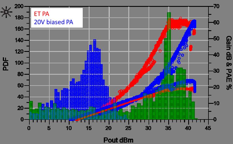
41 The heat advantage: example S-band PA Drive modulated conditions Same W-CDMA signal Same PA Constant 32V V dd Achieves similar linearity Power consumption - 43% less power - 75% longer from battery Power dissipation - 61% less heat RF transistor operates 86% cooler Drive (A) Optimized Vdd Peak/Average Power 40W / 8.5W 40W / 8.5W RFPA drain eff. 30% 76% SM efficiency N/A 69% ACP at 5 / 10MHz -57/-58.3 dbc -55.7/-57.8dBc Transmitter efficiency 30% 52.5% Supply power 28.3W 16.4W


42 What if the antenna is not matched? P dc P in Circulator P out Baseband Signal LO Modulated Carrier Driver Amplifier PA P diss P refl Γ L P tx 42


43 Matching the antenna Supply Circuit DAC P dig P dc Control ADC DAC P in P out Baseband Signal LO Modulated Carrier Driver Amplifier PA Coupler/ Detector P refl Γ L Tuner P tx 43


44 Efficiency improvement 44
Microscale Power Conversion (MPC)
") Microscale Power Conversion (MPC) Quarterly Review Telecon June 30, 2014 University of Colorado, Boulder and TriQuint Semiconductor Co-PIs: Zoya Popovic, Dragan Maksimovic UC-Boulder: Dr. David Sardin,
Microscale Power Conversion (MPC) Quarterly Review Telecon June 30, 2014 University of Colorado, Boulder and TriQuint Semiconductor Co-PIs: Zoya Popovic, Dragan Maksimovic UC-Boulder: Dr. David Sardin,
drain supply terminal impedance at signal envelope frequencies
 WSM: Characterization of transistor drain supply terminal impedance at signal envelope frequencies Zoya Popovic, Scott Schafer, David Sardin, Tibault Reveyrand * University it of Colorado, Boulder *XLIM,
Evaluation of High Efficiency PAs for use in
 CENTRE Evaluation of High Efficiency PAs for use in Supply- and Load-Modulation Transmitters Christian Fager, Hossein Mashad Nemati, Ulf Gustavsson,,* Rik Jos, and Herbert Zirath GigaHertz centre Chalmers
Analyzing Device Behavior at the Current Generator Plane of an Envelope Tracking Power Amplifier in a High Efficiency Mode
 Analyzing Device Behavior at the Current Generator Plane of an Envelope Tracking Power Amplifier in a High Efficiency Mode Z. Mokhti, P.J. Tasker and J. Lees Centre for High Frequency Engineering, Cardiff
Prepared for the Engineers of Samsung Electronics RF transmitter & power amplifier
 Prepared for the Engineers of Samsung Electronics RF transmitter & power amplifier Changsik Yoo Dept. Electrical and Computer Engineering Hanyang University, Seoul, Korea 1 Wireless system market trends
System Considerations for Efficient and Linear Supply Modulated RF Transmitters
 System Considerations for Efficient and Linear Supply Modulated RF Transmitters John Hoversten Department of Electrical and Computer Engineering University of Colorado at Boulder Boulder, Colorado 839
MECXQMM-60W. 8.3 to 10.3 GHz GaN HEMT Power Amplifier
 Pout (dbm), PAE(%) Functional Block Diagram Main Features 0.25µm GaN HEMT Technology 8.3 10.3 GHz full performances Frequency Range 60W Output Power @ Pin 40.5 dbm PAE > 33% @ Pin 40.5 dbm Linear Gain
GaN Power Amplifiers for Next- Generation Wireless Communications
 GaN Power Amplifiers for Next- Generation Wireless Communications Jennifer Kitchen Arizona State University Students: Ruhul Hasin, Mahdi Javid, Soroush Moallemi, Shishir Shukla, Rick Welker Wireless Communications
Energy Efficient Transmitters for Future Wireless Applications
 Energy Efficient Transmitters for Future Wireless Applications Christian Fager christian.fager@chalmers.se C E N T R E Microwave Electronics Laboratory Department of Microtechnology and Nanoscience Chalmers
RF Power Amplifiers for Wireless Communications
 RF Power Amplifiers for Wireless Communications Second Edition Steve C. Cripps ARTECH HOUSE BOSTON LONDON artechhouse.com Contents Preface to the Second Edition CHAPTER 1 1.1 1.2 Linear RF Amplifier Theory
Parallel Doherty RF Power Amplifier. For WiMAX Applications. Sumit Bhardwaj
 Parallel Doherty RF Power Amplifier For WiMAX Applications by Sumit Bhardwaj A Thesis Presented in Partial Fulfillment of the Requirements for the Degree Master of Science Approved November 2018 by the
Gallium Nitride MMIC Power Amplifier
 Gallium Nitride MMIC Power Amplifier August 2015 Rev 4 DESCRIPTION AMCOM s is an ultra-broadband GaN MMIC power amplifier. It has 21dB gain, and >41dBm output power over the 0.03 to 6GHz band. This MMIC
Load Pull Validation of Large Signal Cree GaN Field Effect Transistor (FET) Model
 Model") APPLICATION NOTE Load Pull Validation of Large Signal Cree GaN Field Effect Transistor (FET) Model Introduction Large signal models for RF power transistors, if matched well with measured performance,
APPLICATION NOTE Load Pull Validation of Large Signal Cree GaN Field Effect Transistor (FET) Model Introduction Large signal models for RF power transistors, if matched well with measured performance,
D1H010DA1 10 W, 6 GHz, GaN HEMT Die
 D1H010DA1 10 W, 6 GHz, GaN HEMT Die D1H010DA1 by Dynax is a Gallium Nitride (GaN) high electron mobility transistor (HEMT). The D1H010DA1, operating at 48 V, offers high efficiency, great gain, easy of
Design of Class F Power Amplifiers Using Cree GaN HEMTs and Microwave Office Software to Optimize Gain, Efficiency, and Stability
 White Paper Design of Class F Power Amplifiers Using Cree GaN HEMTs and Microwave Office Software to Optimize Gain, Efficiency, and Stability Overview This white paper explores the design of power amplifiers
Future Networks Webinar Series
 Future Networks Webinar Series Mitigating Thermal & Power Limitations to Enable 5G Presented By Earl McCune, CTO Eridan Communications Wednesday, October 24, 2018 OVERVIEW 5G New Radio modulation Heat
GaN HPA optimized for telecom - Linearity results & DPD assessment March 2017
 GaN HPA optimized for telecom - Linearity results & DPD assessment March 2017 christophe.auvinet@ums-gaas.com GaN technology toward 5G 1. Toward 5G with GaN 2. AB class HPA optimization 3. Doherty linearity
Today s wireless system
 From May 2009 High Frequency Electronics Copyright 2009 Summit Technical Media, LLC High-Power, High-Efficiency GaN HEMT Power Amplifiers for 4G Applications By Simon Wood, Ray Pengelly, Don Farrell, and
QPD0020S2. 35 W, 48 V, DC 6 GHz, GaN RF Power Transistor. Product Overview. Key Features. Functional Block Diagram. Applications. Ordering Information
 Product Overview The is a 35 W unmatched discrete GaN on SiC HEMT which operates from DC to 6 GHz on a +48 V supply rail. It is ideally suited for base station, radar and communications applications and
NPA105-D. Preliminary GHz GaN 40W Power Amplifier. Product Description: Key Features:
 Product Description: The Nxbeam is a Ku-band high power GaN MMIC fabricated in 0.2um GaN HEMT on SiC. This part is ideally suited for satellite communications, point-to-point radios, and radar applications.
High Power Two- Stage Class-AB/J Power Amplifier with High Gain and
 MPRA Munich Personal RePEc Archive High Power Two- Stage Class-AB/J Power Amplifier with High Gain and Efficiency Fatemeh Rahmani and Farhad Razaghian and Alireza Kashaninia Department of Electronics,
Wideband Reconfigurable Harmonically Tuned GaN SSPA for Cognitive Radios
 The University Of Cincinnati College of Engineering Wideband Reconfigurable Harmonically Tuned GaN SSPA for Cognitive Radios Seth W. Waldstein The University of Cincinnati-Main Campus Miguel A. Barbosa
ARFTG 84th WORKSHOP The New Frontiers for Microwave Measurements
 84 th ARFTG Microwave Measurement Conference ARFTG 84th WORKSHOP The New Frontiers for Microwave Measurements December 5 th, 2014 Boulder, Colorado St Julien Hotel 84 th ARFTG Topic: High Efficiency Microwave
10W Ultra-Broadband Power Amplifier
 (TH1B-01 ) 10W Ultra-Broadband Power Amplifier Amin K. Ezzeddine and Ho. C. Huang AMCOM Communications, Inc 401 Professional Drive, Gaithersburg, MD 20879, USA Tel: 301-353-8400 Email: amin@amcomusa.com
AM003536WM-BM-R AM003536WM-EM-R AM003536WM-FM-R
 AM003536WM-BM-R AM003536WM-EM-R AM003536WM-FM-R DESCRIPTION AMCOM s is an ultra-broadband GaAs MMIC power amplifier. It has 22 db gain and 36dBm output power over the 0.01 to 3.5 GHz band. This MMIC is
it to 18 GHz, 2-W Amplifier
 it218 to 18 GHz, 2-W Amplifier Description Features Absolute Maximum Ratings Electrical Characteristics (at 2 C) -ohm system V DD = 8 V Quiescent current (I DQ = 1.1 A The it218 is a three-stage, high-power
AM003536WM-BM-R AM003536WM-FM-R
 AM0036WM-BM-R AM0036WM-FM-R DESCRIPTION AMCOM s is an ultra broadband GaAs MMIC power amplifier. It has 23 db gain, and 36 dbm output power over the 0.01 to 3.5 GHz band. This MMIC is in a ceramic package
Class E and Class D -1 GaN HEMT Switched-Mode Power Amplifiers
 Class E and Class D -1 GaN HEMT Switched-Mode Power Amplifiers J. A. GARCÍA *, R. MERLÍN *, M. FERNÁNDEZ *, B. BEDIA *, L. CABRIA *, R. MARANTE *, T. M. MARTÍN-GUERRERO ** *Departamento Ingeniería de Comunicaciones
MECGaNC30. 4 to 6 GHz GaN HEMT Power Amplifier. Main Features. Product Description. Applications
 Main Features 0.25µm GaN HEMT Technology 4.1 5.9 GHz full performances Frequency Range W Output Power @ Pin 27.5 dbm 37% PAE @ Pin 27.5 dbm % PAE @ Pout Watt 27 db Small Signal Gain Product Description
NPA110-D. Preliminary GHz GaN 38W Power Amplifier. Product Description: Key Features:
 NPA1-D Product Description: The Nxbeam NPA1-D is a Ka-band high power GaN MMIC fabricated in.2um GaN HEMT on SiC. This part is ideally suited for satellite communications, point-to-point radios, and radar
60 W, DC MHz, 50 V, GaN HEMT for LTE and Pulse Radar Applications. = 25 C) of Demonstration Amplifier
 of Demonstration Amplifier") CGHV27060MP 60 W, DC - 2700 MHz, 50 V, GaN HEMT for LTE and Pulse Radar Applications Cree s CGHV27060MP is a 60W gallium nitride (GaN) high electron mobility transistor (HEMT) housed in a small plastic
CGHV27060MP 60 W, DC - 2700 MHz, 50 V, GaN HEMT for LTE and Pulse Radar Applications Cree s CGHV27060MP is a 60W gallium nitride (GaN) high electron mobility transistor (HEMT) housed in a small plastic
Efficiency Enhancement of Pico-cell Base Station Power Amplifier MMIC in GaN HFET Technology Using the Doherty technique
 Efficiency Enhancement of Pico-cell Base Station Power Amplifier MMIC in GaN HFET Technology Using the Doherty technique Sashieka Seneviratne A thesis presented to Ottawa Carleton Institute for Electrical
= 25 C), CW. Parameter 1.7 GHz 1.8 GHz 1.9 GHz Units Small Signal Gain db P in. = 38 dbm
, CW. Parameter 1.7 GHz 1.8 GHz 1.9 GHz Units Small Signal Gain db P in. = 38 dbm") CGHV4PP W, 5 V, GaN HEMT Cree s CGHV4PP is an unmatched, gallium nitride (GaN) high electron mobility transistor (HEMT). The CGHV4PP, operating from a 5 volt rail, offers a general purpose, broadband solution
CGHV4PP W, 5 V, GaN HEMT Cree s CGHV4PP is an unmatched, gallium nitride (GaN) high electron mobility transistor (HEMT). The CGHV4PP, operating from a 5 volt rail, offers a general purpose, broadband solution
Leveraging High-Accuracy Models to Achieve First Pass Success in Power Amplifier Design
 Application Note Leveraging High-Accuracy Models to Achieve First Pass Success in Power Amplifier Design Overview Nonlinear transistor models enable designers to concurrently optimize gain, power, efficiency,
MMA GHz 4W MMIC Power Amplifier Data Sheet
 Features: Frequency Range: 27 33 GHz P1dB: +36 dbm IM3 Level: -38 dbc @Po=20dBm/tone Gain: 22 db Vdd = 6V Idsq = 1500 to 2800mA Input and Output Fully Matched to 50 1 2 3 4 5 32 31 30 29 28 27 26 25 24
Pulse IV and pulsed S-parameter Parametric Analysis with AMCAD PIV & AGILENT PNA-X
 Pulse IV and pulsed S-parameter Parametric Analysis with AMCAD PIV & AGILENT PNA-X Tony Gasseling gasseling@amcad-engineering.com 1 Components PA Design Flow Measurement system Measurement Data base Circuits
= 25 C), CW. Parameter 1.7 GHz 1.8 GHz 1.9 GHz Units Small Signal Gain db P in. = 38 dbm
, CW. Parameter 1.7 GHz 1.8 GHz 1.9 GHz Units Small Signal Gain db P in. = 38 dbm") CGHV42PP 2 W, 5 V, GaN HEMT Cree s CGHV42PP is an unmatched, gallium nitride (GaN) high electron mobility transistor (HEMT). The CGHV42PP, operating from a 5 volt rail, offers a general purpose, broadband
CGHV42PP 2 W, 5 V, GaN HEMT Cree s CGHV42PP is an unmatched, gallium nitride (GaN) high electron mobility transistor (HEMT). The CGHV42PP, operating from a 5 volt rail, offers a general purpose, broadband
In modern wireless. A High-Efficiency Transmission-Line GaN HEMT Class E Power Amplifier CLASS E AMPLIFIER. design of a Class E wireless
 CASS E AMPIFIER From December 009 High Frequency Electronics Copyright 009 Summit Technical Media, C A High-Efficiency Transmission-ine GaN HEMT Class E Power Amplifier By Andrei Grebennikov Bell abs Ireland
TGF Watt Discrete Power GaN on SiC HEMT. Key Features. Measured Performance. Primary Applications Space Military Broadband Wireless
 6 Watt Discrete Power GaN on SiC HEMT Key Features Frequency Range: DC - 18 GHz > 38 dbm Nominal Psat 55% Maximum PAE 15 db Nominal Power Gain Bias: Vd = 28-40 V, Idq = 125 ma, Vg = -3 V Typical Technology:
Introduction to Envelope Tracking. G J Wimpenny Snr Director Technology, Qualcomm UK Ltd
 Introduction to Envelope Tracking G J Wimpenny Snr Director Technology, Qualcomm UK Ltd Envelope Tracking Historical Context EER first proposed by Leonard Kahn in 1952 to improve efficiency of SSB transmitters
27-31 GHz 2W Balanced Power Amplifier TGA4513-CP
 27-31 GHz 2W Balanced Power Amplifier Key Features 27-31 GHz Bandwidth > 32 dbm Nominal P1dB 33 dbm Nominal Psat 22 db Nominal Gain IMD3 is 32 dbc @ 18 dbm SCL 12 db Nominal Return Loss Bias: 6 V, 84 ma
NPA100-D GHz GaN 20W Power Amplifier. Product Description: Key Features:
 Product Description: The Nxbeam is a Ku-band high power GaN MMIC fabricated in 0.2um GaN HEMT on SiC. This part is ideally suited for satellite communications, point-to-point radios, and radar applications.
A 2.4-GHz 24-dBm SOI CMOS Power Amplifier with Fully Integrated Output Balun and Switched Capacitors for Load Line Adaptation
 A 2.4-GHz 24-dBm SOI CMOS Power Amplifier with Fully Integrated Output Balun and Switched Capacitors for Load Line Adaptation Francesco Carrara 1, Calogero D. Presti 2,1, Fausto Pappalardo 1, and Giuseppe
QPD0210TR7. 2x15 W, 48 V, GHz, Dual GaN RF Transistor. Product Overview. Applications. Functional Block Diagram. Ordering Information
 Product Overview The is a dual-path discrete GaN on SiC HEMT in a DFN package which operates from 1.8 to 2.7 GHz. In each path is a single-stage amplifier transistor. can deliver PSAT of 16.6 W at +48
CG2H W, DC - 6 GHz, RF Power GaN HEMT APPLICATIONS FEATURES
 Rev 0.0 May 2017 CG2H40010 10 W, DC - 6 GHz, RF Power GaN HEMT Cree s CG2H40010 is an unmatched, gallium nitride (GaN) high electron mobility transistor (HEMT). The CG2H40010, operating from a 28 volt
The Design of A 125W L-Band GaN Power Amplifier
 Sheet Code RFi0613 White Paper The Design of A 125W L-Band GaN Power Amplifier This paper describes the design and evaluation of a single stage 125W L-Band GaN Power Amplifier using a low-cost packaged
27-31 GHz 2W Balanced Power Amplifier TGA4513
 27-31 GHz 2W Balanced Power Amplifier Key Features 27-31 GHz Bandwidth > 32 dbm P1dB 33 dbm Psat 2 db Nominal Gain IMR3 is 37 dbc @ 18 dbm SCL 14 db Nominal Return Loss Bias: 6 V, 84 ma.25 um 3MI MMW phemt
85W Power Transistor. GaN HEMT on SiC
 GaN HEMT on SiC Description The is a 85W Gallium Nitride High Electron Mobility Transistor. This product offers a general purpose and broadband solution for a variety of RF power applications such as radar
GaAs MMIC Power Amplifier
 GaAs MMIC Power Amplifier AM83WM-BM-R AM83WM-FM-R March 211 Rev 1 DESCRIPTION AMCOM s AM83WM-BM/FM-R is an ultra broadband GaAs MMIC power amplifier. It has 23dB gain, and >28dBm output power over the.
Silicon-Carbide High Efficiency 145 MHz Amplifier for Space Applications
 Silicon-Carbide High Efficiency 145 MHz Amplifier for Space Applications By Marc Franco, N2UO 1 Introduction This paper describes a W high efficiency 145 MHz amplifier to be used in a spacecraft like AMSAT
10 W, GaN Power Amplifier, 2.7 GHz to 3.8 GHz HMC1114
 9 13 16 FEATURES High saturated output power (PSAT): 41.5 dbm typical High small signal gain: db typical High power gain for saturated output power:.5 db typical Bandwidth: 2.7 GHz to 3.8 GHz High power
Efficiency Enhancement of CDMA Power Amplifiers in Mobile Handsets Using Dynamic Supplies. Georgia Tech Analog Consortium Presentation
 Efficiency Enhancement of CDMA Power Amplifiers in Mobile Handsets Using Dynamic Supplies Biranchinath Sahu Advisor: Prof. Gabriel A. Rincón-Mora Analog Integrated Circuits Laboratory School of Electrical
An RF-input outphasing power amplifier with RF signal decomposition network
 An RF-input outphasing power amplifier with RF signal decomposition network The MIT Faculty has made this article openly available. Please share how this access benefits you. Your story matters. Citation
6-18 GHz High Power Amplifier TGA9092-SCC
 6-18 GHz High Power Amplifier Key Features and Performance Dual Channel Power Amplifier 0.25um phemt Technology 6-18 GHz Frequency Range 2.8 W/Channel Midband Pout 5.6 W Pout Combined 24 db Nominal Gain
= 25 C) of Demonstration Amplifier. Parameter 2.3 GHz 2.4 GHz 2.5 GHz 2.6 GHz 2.7 GHz Units. 43 dbm
 of Demonstration Amplifier. Parameter 2.3 GHz 2.4 GHz 2.5 GHz 2.6 GHz 2.7 GHz Units. 43 dbm") Rev 3.1 - June 2015 CGH25120F 120 W, 2300-2700 MHz, GaN HEMT for WiMAX and LTE Cree s CGH25120F is a gallium nitride (GaN) high electron mobility transistor (HEMT) designed specifically for high efficiency,
Rev 3.1 - June 2015 CGH25120F 120 W, 2300-2700 MHz, GaN HEMT for WiMAX and LTE Cree s CGH25120F is a gallium nitride (GaN) high electron mobility transistor (HEMT) designed specifically for high efficiency,
GaAs MMIC Power Amplifier
 GaAs MMIC Power Amplifier AM83WM-BM-R AM83WM-FM-R December 214 REV DESCRIPTION AMCOM s AM83WM-BM/FM-R is an ultra broadband GaAs MMIC power amplifier. It has 23dB gain, and >28dBm output power over the.
High Efficiency Class-F MMIC Power Amplifiers at Ku-Band
 High Efficiency Class-F MMIC Power Amplifiers at Ku-Band Matthew T. Ozalas The MITRE Corporation 2 Burlington Road, Bedford, MA 173 mozalas@mitre.org Abstract Two high efficiency Ku-band phemt power amplifier
TGA2622-CP 9 10 GHz 35 W GaN Power Amplifier
 9 1 GHz W GaN Power Amplifier Applications Weather and Marine Radar Product Features Frequency Range: 9 1 GHz PSAT:.5 dbm @ PIN = 18 dbm PAE: >% @ PIN = 18 dbm Power Gain: 27.5 db @ PIN = 18 dbm Bias:
MMA GHz, 0.1W Gain Block Data Sheet
 Features: Frequency Range: 6 22 GHz P1dB: 18.5 dbm @Vds=5V Psat: 19.5 dbm @ Gain: 14 db Vdd =3 to 6 V Ids = 13 ma Input and Output Fully Matched to 5 Ω Applications: Communication systems Microwave instrumentations
PTFB193404F. Thermally-Enhanced High Power RF LDMOS FET 340 W, 30 V, MHz. Description. Features. RF Characteristics
 PTFB9404F Thermally-Enhanced High Power RF LDMOS FET 40 W, 0 V, 90 990 MHz Description The PTFB9404F is a 40 watt LDMOS FET intended for use in multi-standard cellular power amplifier applications in the
Gallium Nitride MMIC Power Amplifier
 Gallium Nitride MMIC Power Amplifier AM47TM- AM47SD-2H August 15 Rev 2 DESCRIPTION AMCOM s AM47TM- is an ultra-broadband GaN MMIC power amplifier. It has db gain, and >46dBm output power over the.3 to
Stuart Glynn Power Amplifier Design Engineer
 Stuart Glynn Power Amplifier Design Engineer Keysight Technologies 2017 How to Design an X-band MMIC PA Stuart Glynn and Liam Devlin Introduction Target specification and application Design approach Device
GaAs, phemt, MMIC, Single Positive Supply, DC to 7.5 GHz, 1 W Power Amplifier HMC637BPM5E
 9 11 13 31 NIC 3 ACG1 29 ACG2 2 NIC 27 NIC 26 NIC GaAs, phemt, MMIC, Single Positive Supply, DC to 7.5 GHz, 1 W Power Amplifier FEATURES P1dB output power: 2 dbm typical Gain:.5 db typical Output IP3:
Efficiency (%) Characteristic Symbol Min Typ Max Units
 Characteristic Symbol Min Typ Max Units") PTF181 LDMOS RF Power Field Effect Transistor W, 185 188 MHz, 193 199 MHz W, 21 217 MHz Description Features The PTF181 is a W, internally matched GOLDMOS FET device intended for EDGE applications in the
PTF181 LDMOS RF Power Field Effect Transistor W, 185 188 MHz, 193 199 MHz W, 21 217 MHz Description Features The PTF181 is a W, internally matched GOLDMOS FET device intended for EDGE applications in the
Efficiency (%) Characteristic Symbol Min Typ Max Unit. Adjacent Channel Power Ratio ACPR dbc
 Characteristic Symbol Min Typ Max Unit. Adjacent Channel Power Ratio ACPR dbc") GTRA36282FC Thermally-Enhanced High Power RF GaN on SiC HEMT 28 W, 48 V, 34 36 MHz Description The GTRA36282FC is a 28-watt ( ) GaN on SiC high electron mobility transistor (HEMT) designed for use in multi-standard
GTRA36282FC Thermally-Enhanced High Power RF GaN on SiC HEMT 28 W, 48 V, 34 36 MHz Description The GTRA36282FC is a 28-watt ( ) GaN on SiC high electron mobility transistor (HEMT) designed for use in multi-standard
Advance Datasheet Revision: April 2015
 APN 1-1 GHz Advance Datasheet Revision: April Applications Point-to-Point Digital Radios Point-to-Multipoint Digital Radios VSAT Test Instrumentation X = 3 um Y = 3 um Product Features RF frequency: 1
A Testbench for Analysis of Bias Network Effects in an RF Power Amplifier with DPD. Marius Ubostad and Morten Olavsbråten
 A Testbench for Analysis of Bias Network Effects in an RF Power Amplifier with DPD Marius Ubostad and Morten Olavsbråten Dept. of Electronics and Telecommunications Norwegian University of Science and
Introducing the High Voltage Vertical Technology for High Power Applications
 Introducing the High Voltage Vertical Technology for High Power Applications Brian D. Battaglia Applications Engineering HVVi Semiconductors Phoenix, AZ Page 1 AGENDA Background Device Overview Packaging
FP Description. Features. Applications. Packaging Information. 50W, 28V GaN HEMT Die
 FP28010060 50W, 28V GaN HEMT Die Description The FP28010060 is a 50W gallium nitride (GaN) High Electron Mobility Transistor (HEMT). This GaN HEMT is a wideband transistor optimized for X-band operation
Efficiency (%) Characteristic Symbol Min Typ Max Unit. Adjacent Channel Power Ratio ACPR dbc. Output 0.01% CCDF OPAR 7 7.
 Characteristic Symbol Min Typ Max Unit. Adjacent Channel Power Ratio ACPR dbc. Output 0.01% CCDF OPAR 7 7.") Thermally-Enhanced High Power RF GaN on SiC HEMT W, 48 V, 34 36 MHz Description The is a -watt (P3dB) GaN on SiC high electron mobility transistor (HEMT) designed for use in multi-standard cellular power
Thermally-Enhanced High Power RF GaN on SiC HEMT W, 48 V, 34 36 MHz Description The is a -watt (P3dB) GaN on SiC high electron mobility transistor (HEMT) designed for use in multi-standard cellular power
Efficiency (%) gtra364002fc_g1. Characteristic Symbol Min Typ Max Unit. Adjacent Channel Power Ratio ACPR dbc
 gtra364002fc_g1. Characteristic Symbol Min Typ Max Unit. Adjacent Channel Power Ratio ACPR dbc") Thermally-Enhanced High Power RF GaN on SiC HEMT 0 W, 48 V, 30 30 MHz Description The is a 0-watt (PSAT) GaN on SiC high electron mobility transistor (HEMT) designed for use in multi-standard cellular
Thermally-Enhanced High Power RF GaN on SiC HEMT 0 W, 48 V, 30 30 MHz Description The is a 0-watt (PSAT) GaN on SiC high electron mobility transistor (HEMT) designed for use in multi-standard cellular
Introduction to Surface Acoustic Wave (SAW) Devices
 Devices") May 31, 2018 Introduction to Surface Acoustic Wave (SAW) Devices Part 7: Basics of RF Circuits Ken-ya Hashimoto Chiba University k.hashimoto@ieee.org http://www.te.chiba-u.jp/~ken Contents Noise Figure
May 31, 2018 Introduction to Surface Acoustic Wave (SAW) Devices Part 7: Basics of RF Circuits Ken-ya Hashimoto Chiba University k.hashimoto@ieee.org http://www.te.chiba-u.jp/~ken Contents Noise Figure
DESIGN OF AN S-BAND TWO-WAY INVERTED ASYM- METRICAL DOHERTY POWER AMPLIFIER FOR LONG TERM EVOLUTION APPLICATIONS
 Progress In Electromagnetics Research Letters, Vol. 39, 73 80, 2013 DESIGN OF AN S-BAND TWO-WAY INVERTED ASYM- METRICAL DOHERTY POWER AMPLIFIER FOR LONG TERM EVOLUTION APPLICATIONS Hai-Jin Zhou * and Hua
Concurrent Multi-Band Envelope Tracking Power Amplifiers for Emerging Wireless Communications
 Concurrent Multi-Band Envelope Tracking Power Amplifiers for Emerging Wireless Communications by Hassan Sarbishaei A thesis presented to the University of Waterloo in fulfillment of the thesis requirement
POSTECH Activities on CMOS based Linear Power Amplifiers
 1 POSTECH Activities on CMOS based Linear Power Amplifiers Jan. 16. 2006 Bumman Kim, & Jongchan Kang MMIC Laboratory Department of EE, POSTECH Presentation Outline 2 Motivation Basic Design Approach CMOS
GaN MMIC PAs for MMW Applicaitons
 GaN MMIC PAs for MMW Applicaitons Miroslav Micovic HRL Laboratories LLC, 311 Malibu Canyon Road, Malibu, CA 9265, U. S. A. mmicovic@hrl.com Motivation for High Frequency Power sources 6 GHz 11 GHz Frequency
FP Description. Features. Applications. Packaging Information. 104W, 48V GaN HEMT D
 FP48007104 104W, 48V GaN HEMT D Description The FP48007104 is a 104W gallium nitride (GaN) High Electron Mobility Transistor (HEMT). This GaN HEMT is a wideband transistor optimized for 3.5GHz operation
1 GHz Current Mode Class-D Power Amplifier in Hybrid Technology Using GaN HEMTs
 ROMANIAN JOURNAL OF INFORMATION SCIENCE AND TECHNOLOGY Volume 11, Number 4, 2008, 319 328 1 GHz Current Mode Class-D Power Amplifier in Hybrid Technology Using GaN HEMTs Pouya AFLAKI, Renato NEGRA, Fadhel
GaAs MMIC Power Amplifier for VSAT & ITU Applications
 GaAs MMIC Power Amplifier for VSAT & ITU Applications AM1351642WM-XX-R April 216 Rev 4 DESCRIPTION AMCOM s AM1351642WM--R is a Ku-band GaAs MMIC power amplifier designed for VSAT ground station transmitter
Type Marking Ordering code (taped) CGY 180 CGY 180 Q68000-A8882 MW 12
 CGY 180 CGY 180 Q68000-A8882 MW 12") Datasheet * Power amplifier for DECT and PCS application * Fully integrated 3 stage amplifier * Operating voltage range: 2.7 to 6 V * Overall power added efficiency 35 % * Input matched to 5 Ω, simple
Datasheet * Power amplifier for DECT and PCS application * Fully integrated 3 stage amplifier * Operating voltage range: 2.7 to 6 V * Overall power added efficiency 35 % * Input matched to 5 Ω, simple
Title: New High Efficiency Intermodulation Cancellation Technique for Single Stage Amplifiers.
 Title: New High Efficiency Intermodulation Cancellation Technique for Single Stage Amplifiers. By: Ray Gutierrez Micronda LLC email: ray@micronda.com February 12, 2008. Introduction: This article provides
400 MHz to 4000 MHz ½ Watt RF Driver Amplifier ADL5324
 Data Sheet FEATURES Operation from MHz to MHz Gain of 14.6 db at 21 MHz OIP of 4.1 dbm at 21 MHz P1dB of 29.1 dbm at 21 MHz Noise figure of.8 db Dynamically adjustable bias Adjustable power supply bias:.
A balancing act: Envelope Tracking and Digital Pre-Distortion in Handset Transmitters
 Abstract Envelope tracking requires the addition of another connector to the RF power amplifier. Providing this supply modulation input leads to many possibilities for improving the performance of the
maintaining high gain and efficiency. Parameter 5.5 GHz 6.0 GHz 6.5 GHz Units Small Signal Gain db = 28 dbm
 CGHVF006S 6 W, DC - 5 GHz, 40V, GaN HEMT Cree s CGHVF006S is an unmatched, gallium nitride (GaN) high electron mobility transistor (HEMT) designed specifically for high efficiency, high gain and wide bandwidth
DC - 20 GHz Discrete power phemt
 DC - 20 GHz Discrete power phemt Product Description The TriQuint is a discrete 0.6 mm phemt which operates from DC-20 GHz. The is designed using TriQuint s proven standard 0.3um power phemt production
Ray Pengelly, Cree RF and Microwave Products, Research Triangle Park, NC October 21, 2010
 Ray Pengelly, Cree RF and Microwave Products, Research Triangle Park, NC 27709 October 21, 2010 Agenda GaN HEMT Transistor Structures High Power Densities Blessing or Curse? Thermal Management CW, Pulsed
A new nonlinear HEMT model allowing accurate simulation of very low IM 3 levels for high-frequency highly linear amplifiers design
 A new nonlinear HEMT model allowing accurate simulation of very low IM 3 levels for high-frequency highly linear amplifiers design J. Lhortolary 1, C. Chang 1, T. Reveyrand 2, M. Camiade 1, M. Campovecchio
InAlN/GaN HEMTs Technologies for Microwave, Fast switching and Mixed Signal Applications
 InAlN/GaN HEMTs Technologies for Microwave, Fast switching and Mixed Signal Applications S.DELAGE / S.PIOTROWICZ Summary III-V Lab presentation Motivations Technology for L & S band applications Technology
MMA M GHz, 1W MMIC Power Amplifier Data Sheet
 Features: Frequency Range: 37-41 GHz P1dB: +30.5 dbm IM3 Level: -41 dbc @Po=18dBm/tone Gain: 22 db Vdd = 4 to 6 V Idsq = 1000 to 2000 ma Input and Output Fully Matched to 50 Ω Integrated power detector
MMA M GHz 4W MMIC Power Amplifier Data Sheet
 Features: Frequency Range: 27 33 GHz P1dB: +36 dbm IM3 Level: -38 dbc @Po=20dBm/tone Gain: 22 db Vdd = 6V Idsq = 1500 to 2800mA Input and Output Fully Matched to 50 Ω Surface Mount, RoHs Compliant QFN
TGF Watt Discrete Power GaN on SiC HEMT
 Applications Marine radar Satellite communications Point to point communications Military communications Broadband amplifiers High efficiency amplifiers Product Features Functional Block Diagram Frequency
Reinventing the Transmit Chain for Next-Generation Multimode Wireless Devices. By: Richard Harlan, Director of Technical Marketing, ParkerVision
 Reinventing the Transmit Chain for Next-Generation Multimode Wireless Devices By: Richard Harlan, Director of Technical Marketing, ParkerVision Upcoming generations of radio access standards are placing
Efficiency (%) g261701fa-gr1a. Characteristic Symbol Min Typ Max Unit. Adjacent Channel Power Ratio ACPR dbc
 g261701fa-gr1a. Characteristic Symbol Min Typ Max Unit. Adjacent Channel Power Ratio ACPR dbc") g26171fa-gr1a GTVA26171FA Thermally-Enhanced High Power RF GaN on SiC HEMT 17 W, 5 V, 26 269 MHz Description The GTVA26171FA is a 17-watt (P 3dB ) GaN on SiC high electron mobility transistor (HEMT) for
g26171fa-gr1a GTVA26171FA Thermally-Enhanced High Power RF GaN on SiC HEMT 17 W, 5 V, 26 269 MHz Description The GTVA26171FA is a 17-watt (P 3dB ) GaN on SiC high electron mobility transistor (HEMT) for
MMA GHz, 0.1W Gain Block
 Total Size: 172 x 76 Scribe Alley: 7 x 7 MMA-174321 Features: Frequency Range: 17 43 GHz P1dB: 21 dbm Psat: 22 dbm Gain: 22 db Vdd =5 V (3 V to 5 V) Ids = 2 ma (15mA to 3mA) Input and Output Fully Matched
MMA R GHz 4W MMIC Power Amplifier Data Sheet Old package not recommended for new designs
 Old package not recommended for new designs Features: Frequency Range: 28-31 GHz P1dB: +36 dbm IM3 Level: -35 dbc @Po=26dBm/tone Gain: 22 db Vdd = 5 to 6V Idsq = 1200 to 3000mA Input and Output Fully Matched
ABSOLUTE MAXIMUM RATINGS (Case Temperature Tc=25deg.C) Item Symbol Condition Rating Unit Operating-Voltage VDS 55 V. Item Symbol Condition Limit Unit
 Item Symbol Condition Rating Unit Operating-Voltage VDS 55 V. Item Symbol Condition Limit Unit") FEATURES High Voltage Operation : VDS=V High Power :.5dBm (typ.) @ Psat High Efficiency: 65%(typ.) @ Psat Power Gain :19dB(typ.) @ f=1.6ghz Proven Reliability DESCRIPTION SEI's GaN-HEMT offers high efficiency,
FEATURES High Voltage Operation : VDS=V High Power :.5dBm (typ.) @ Psat High Efficiency: 65%(typ.) @ Psat Power Gain :19dB(typ.) @ f=1.6ghz Proven Reliability DESCRIPTION SEI's GaN-HEMT offers high efficiency,
50 GHz to 95 GHz, GaAs, phemt, MMIC, Wideband Power Amplifier ADPA7001CHIPS
 FEATURES Gain:.5 db typical at 5 GHz to 7 GHz S11: db typical at 5 GHz to 7 GHz S: 19 db typical at 5 GHz to 7 GHz P1dB: 17 dbm typical at 5 GHz to 7 GHz PSAT: 1 dbm typical OIP3: 5 dbm typical at 7 GHz
An Outphasing Transmitter Using Class-E PAs and Asymmetric Combining: Part 2
 From May 2011 High Frequency Electronics Copyright 2011 Summit Technical Media, LLC An Outphasing Transmitter Using Class-E PAs and Asymmetric Combining: Part 2 By Ramon Beltran, RF Micro Devices; Frederick
Innogration (Suzhou) Co., Ltd.
 Co., Ltd.") Gallium Nitride 28V 50W, RF Power Transistor Description The GTAH58050GX is a 50W internally matched, GaN HEMT, designed from 5 to 6GHz, especially point-to-point communication, broadband wireless access,
Gallium Nitride 28V 50W, RF Power Transistor Description The GTAH58050GX is a 50W internally matched, GaN HEMT, designed from 5 to 6GHz, especially point-to-point communication, broadband wireless access,
AlGaN Polarization Graded Field Effect Transistors for High Linearity Microwave Applications
 AlGaN Polarization Graded Field Effect Transistors for High Linearity Microwave Applications Shahadat H. Sohel, Hao Xue, Towhidur Razzak, Sanyam Bajaj, Yuewei Zhang, Wu Lu, Siddharth Rajan Department of