This Week s Subject. DRAM & Flexible RRAM. p-channel MOSFET (PMOS) CMOS: Complementary Metal Oxide Semiconductor
|
|
|
- Bethany Chase
- 5 years ago
- Views:
Transcription
1 DRAM & Flexible RRAM This Week s Subject p-channel MOSFET (PMOS) CMOS: Complementary Metal Oxide Semiconductor CMOS Logic Inverter NAND gate NOR gate CMOS Integration & Layout GaAs MESFET (JFET) 1 Flexible Inorganic Semiconductor Technology
2 DRAM (Dynamic Random Access Memory) Schematic DRAM Chip Architecture: Memory Cell Array Col. Dec. Col. Dec. Row Decoder Row Decoder Row Decoder Row Decoder PAD Col. Dec. Col. Dec. 2 RAS (row access strobe) Supplementary
3 DRAM cell (Or Display) Word line Transfer gate [access] 1cm Storage node Bit line Capacitor (or OLED ) Periphery circuits Cell array (core) 3cm DRAM: I/O gate, CMOS TR Data sense/amplifier Data read Data refresh Random access: row decoder Select word line column decoder Select bit line Need to refresh the charge loss in the capacitor (μsec) Display (LCD or OLED): Active Matrix: with transistor in each cell. Fast speed, Large pixel 3 Passive Matrix: w/o transistor. Slow respond speed(~250msec), small pixel
4 p-channel MOSFET Circuit diagram Gate electrode Source electrode Drain electrode Gate -I DS Transfer curve (Id-Vg curve) Vd=-1V Source (p + ) Drain (p + ) Gate oxide n-type Si substrate p-channel MOSFET (PMOS) Id-Vd curve V -V Th =-0.5V -1.8V -V G - 4 -
 Vin Vout 5 Vgn=Vin Vdsn=Vout Vtn=-Vtp Vgp=Vin-Vdd")
5 CMOS Logic (Inverter) Complementary Metal Oxide Semiconductor: NMOS+PMOS Inverter : building block of integrated circuits Reference 1, 0 Pull-up PMOS 0, 1 Pull-down NMOS Reference (Ground) Vin Vout 5 Vgn=Vin Vdsn=Vout Vtn=-Vtp Vgp=Vin-Vdd Vdsp=Vout-Vdd
6 CMOS Logic (Inverter) 1.8V digital 1 0V digital 0 Reference(1.8V) Vgp=Vin-Vdd 1.8V 1.8V Vgp= 0V Vgn=1.8V Vtp=-0.5V off Vtn=0.5V on Pull down by NMOS 0V 100 Ohm 1 Ohm 0V Reference (Ground) Digital 1 is inverted to digital 0 6
7 CMOS Logic (Inverter) 1.8V digital 1 0V digital 0 Reference(1.8V) Vgp=Vin-Vdd 1.8V 0V Vgp= -1.8V Vgn=0V Vtp=-0.5V on Vtn=0.5V off Pull up by PMOS 1.79V 1 Ohm 1.79V 100 Ohm Reference (Ground) Digital 0 is inverted to digital 1 7


8 CMOS Logic (NAND Gate) V DD Pull-up PMOS Pull-down NMOS Pull-down NMOS The output is high when either of inputs A or B is high, or if neither is high. In other words, it is normally high, going low only if both A and B are high. 8


9 CMOS Logic (NOR Gate) V DD Pull-up PMOS Pull-up PMOS Pull-down NMOS The output is high only when neither A nor B is high. That is, it is normally high but any kind of non-zero input will take it low. 9

10 CMOS Inverter Layout 10 Ref: CMOS VLSI Design, N.Weste, Addison Wiley,

11 CMOS Inverter Mask Layout 11
 Initial oxidation Temperature : 1000C 130min.")
 Oxide etch 7:1 BHF 6min f) P/R strip Acetone, IPA, DI wafer g) Well implantation Ion species : P")
12 a) Starting Material Dopant type : p-type (boron) Orientation : (100) Resistivity : 13±2 Wafer size : 4 inch b) Initial oxidation Temperature : 1000C 130min. Thickness : 6000±6000Å d) Well mask PR coat, soft bake Align, Exposure Develop, Hard bake Mask 1 12 e) Oxide etch 7:1 BHF 6min f) P/R strip Acetone, IPA, DI wafer g) Well implantation Ion species : P + Dose : 3.6x10 12 /cm 2 Energy : 120keV
 Poly deposition Temperature : 625 C")
 Poly etch RIE (Plasma")
 13")
13 (h) (i) (j) i) Gate oxidation Temperature : 950 C, 31min. Thickness : 250±20Å i) Poly deposition Temperature : 625 C Thickness : 3500±300Å j) Gate mask P/R coat, soft bake Align, Exposure Develop, CD check Hard bake j) Poly etch RIE (Plasma etching) Mask 2 (k) k) Oxide Growth l) N+ S/D implantation Ion species : As + Dose : 5x10 15 /cm 2 Energy : 80keV (l) 13 Mask 3
 o) N+ S/D implantation Ion species : BF")
 Contact etch RIE : CHF 3 +CF 4 +Ar Mask 5")
14 (m) (n) Repeats using p+ diffusion mask Mask 4 (o) o) N+ S/D implantation Ion species : BF 2 + Dose : 3x10 15 /cm 2 Energy : 40keV (p) p) Contact etch RIE : CHF 3 +CF 4 +Ar Mask 5 14


15 (r) r) Metal deposition Target : Al-1% Si Thickness : 0.7 m r) Metal etch Reactant gas : BCl 3 +Cl 2 RIE Mask 6 15
 1400 3900 8500 30000 p (cm 2 /Vs) 470 1900 400 500")
16 GaAs MESFET MESFET (Metal Semiconductor Field Effect Transistor): one type of JFET(junction field effect transistor) N type GaAs Normally III-V Sc, High mobility, frequency device Si Ge GaAs InAs n (cm 2 /Vs) p (cm 2 /Vs)
")
17 Normally off MESFET (enhancement mode) 17
 BOX Very")


18 Flexible Single Crystal Silicon from SOI Si (100 nm) BOX Very thin and flexible High performance similar to Si VLSI technology Well established technology Appl. Phys. Lett. 84, 5398 (2004) 18


19 Large Area, Selective Transfer of µs-si using PDMS Stamp Contact PDMS stamp µs-si on SOI wafer 1 cm Sacrificial SiO 2 layer 10 mm Mother substrate PET 100 µm 20 cm Transfer µs-si from stamp to PET Remaining SOI wafer 19 Adv. Mater. 17, 2336, 2005


20 High Performance Device on Plastic Substrate I DS (ua) µ= 520 cm 2 /Vs, on/off=10 6 V th = 0.7 V O n E-3 1E-4 1E-5 1E-6 1E-7 I ds (A) 50 0 Off V GS (V) V ds =0.1V 1E-8 1E-9 1E-10 Appl. Phys. Lett. 90, , 2007 IEEE Elect. Device Letters. 27, 460,
 Id-Vd Id-Vg Journal of Applied Physics, 100, 124507 2006")
21 Flexible III-V HEMTs Si-doped AlGaAs - Undoped GaAs (Chap 5.8) Id-Vd Id-Vg Journal of Applied Physics, 100,


22 Flexible 3D Heterogeneous Integration Direct transfer of µs-sc 15 µm µs-gan on Si wafer 3D direct integration Heterogeneous 3D integration on Plastics µs-sc 500 µm Nature Materials, 5, 33, 2006 Science, 314, 1754,


23 Why Flexible Memory? Storage Memory (Essential element) Processing Communication 23 Flexible Electronic Systems


24 Memristor, Missing Fundamental Circuit Element Resistive Random Access Memory (RRAM) First proposed in 1971 Neuromophic Systems. D. Strukov et al., Nature, 453, 80, 2008 Kim, K. IEEE Tech. Dig. IEDM, 1-4, Jo, S.H et al. Nano Lett. 10, 1297, 2010


25 Prior Research of Flexible Resistive Memory Titinium oxide Aluminum oxide Cross-point structure (No switching elements) Graphene oxide GeO/HfO N Cell-to-cell interference Require high performance switching transistor Nanotechnol, APL, Nano Letter, Adv. Mater (µ> 200 cm 2 /Vs)


26 Flexible one transistor-one memristor (1T-1M) memory 26 Nano Lett., 11(12), 5438, 2011


27 1T-1M Structure Circuit Diagram V SET = -2.1 V, V SET = 2.7 V ON/OFF ratio of 50 at -0.5 V (V READ ) 27 Nano Lett., 11(12), 5438, 2011


,")
28 Random Access Operation 28 Nano Lett., 11(12), 5438, 2011

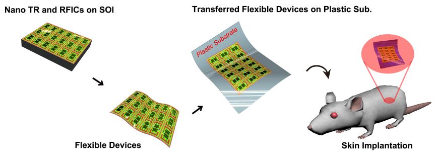
29 Flexible LSI for Implantable Devices 29 Using 0.18µm CMOS ACS Nano, 7, 4545, 2013


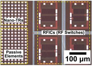
30 Electrical Properties of Flexible Devices RFICs (RF Switches) G S G Input Port M1 M2 Output Port G S G 200 μm 30 Stable Operations on Plastics ACS Nano, 7, 4545, 2013


31 Roll to Roll ACF Packaged Flexible NAND Flash Memory Adv. Mater. 28, 8371, 2016


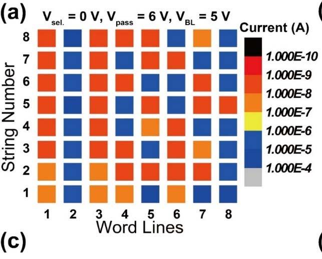
32 Flexible NAND Flash Memory Unit Cell Operation Read voltage Transfer Curve Endurance Retention Adv. Mater. 28, 8371, 2016

")

33 Flexible one selector-one resistor (1S1R) memory Adv. Mater. 26, 7480, 2014


34 Flexible Crossbar Memory using ILLO Adv. Mater. 26, 7480, 2014


35 Flexible Oxide TFTs using ILLO TFT structure IZO thickness of 20 nm GI thickness of 176 nm Adv. Func. Mater. 26, 6170, 2016
 SS (V/dec) 0.31 0.32 V on (V) -0.6-0.7 ΔV (V) 0.015 0.017 *@ 15 V Adv. Func. Mater.")
36 Flexible Oxide TFTs using ILLO Transfer Curve Output Curve On glass On plastic μ* (cm 2 /Vs) Negative Bias (-20 V) SS (V/dec) V on (V) ΔV (V) *@ 15 V Adv. Func. Mater. 26, 6170, 2016
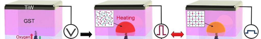
37 Self-Structured Nano-filament for Phase Change Memory ACS Nano 9, 6587, 2015

")


38 Comparison between ILED and OLED ILED(Inorganic) OLED(Organic) Merits Stability High efficiency(2x OLED) Long lifetime(50x OLED) Merits Flexibility Simple process Demerits Rigid & Thick Demerits Short lifetime in humid Low efficiency

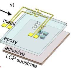
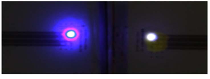
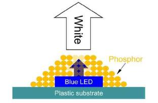
39 Fabrication of Flexible GaN LED Blue White 39 Nano Energy 1, 145, 2012


40 Flexible Vetical micro LED Nano Energy 447, 44, 2018


41 Flexible VLED on Motor Cortex Behavior Control Nano Energy 447, 44, 2018


42 Flexible Monolithic GaN LED Fabrication Process Optical output measurements & Device image Adv. Mater. In press
Transistor was first invented by William.B.Shockley, Walter Brattain and John Bardeen of Bell Labratories. In 1961, first IC was introduced.
 Unit 1 Basic MOS Technology Transistor was first invented by William.B.Shockley, Walter Brattain and John Bardeen of Bell Labratories. In 1961, first IC was introduced. Levels of Integration:- i) SSI:-
Depletion-mode operation ( 공핍형 ): Using an input gate voltage to effectively decrease the channel size of an FET
: Using an input gate voltage to effectively decrease the channel size of an FET") Ch. 13 MOSFET Metal-Oxide-Semiconductor Field-Effect Transistor : I D D-mode E-mode V g The gate oxide is made of dielectric SiO 2 with e = 3.9 Depletion-mode operation ( 공핍형 ): Using an input gate voltage
Ch. 13 MOSFET Metal-Oxide-Semiconductor Field-Effect Transistor : I D D-mode E-mode V g The gate oxide is made of dielectric SiO 2 with e = 3.9 Depletion-mode operation ( 공핍형 ): Using an input gate voltage
Nano-crystalline Oxide Semiconductor Materials for Semiconductor and Display Technology Sanghun Jeon Ph.D. Associate Professor
 Nano-crystalline Oxide Semiconductor Materials for Semiconductor and Display Technology Sanghun Jeon Ph.D. Associate Professor Department of Applied Physics Korea University Personnel Profile (Affiliation
Lecture 0: Introduction
 Lecture 0: Introduction Introduction Integrated circuits: many transistors on one chip. Very Large Scale Integration (VLSI): bucketloads! Complementary Metal Oxide Semiconductor Fast, cheap, low power
420 Intro to VLSI Design
 Dept of Electrical and Computer Engineering 420 Intro to VLSI Design Lecture 0: Course Introduction and Overview Valencia M. Joyner Spring 2005 Getting Started Syllabus About the Instructor Labs, Problem
+1 (479)
") Introduction to VLSI Design http://csce.uark.edu +1 (479) 575-6043 yrpeng@uark.edu Invention of the Transistor Vacuum tubes ruled in first half of 20th century Large, expensive, power-hungry, unreliable
Introduction to VLSI Design http://csce.uark.edu +1 (479) 575-6043 yrpeng@uark.edu Invention of the Transistor Vacuum tubes ruled in first half of 20th century Large, expensive, power-hungry, unreliable
Topic 3. CMOS Fabrication Process
 Topic 3 CMOS Fabrication Process Peter Cheung Department of Electrical & Electronic Engineering Imperial College London URL: www.ee.ic.ac.uk/pcheung/ E-mail: p.cheung@ic.ac.uk Lecture 3-1 Layout of a Inverter
Microelectronics, BSc course
 Microelectronics, BSc course MOS circuits: CMOS circuits, construction http://www.eet.bme.hu/~poppe/miel/en/14-cmos.pptx http://www.eet.bme.hu The abstraction level of our study: SYSTEM + MODULE GATE CIRCUIT
Fin-Shaped Field Effect Transistor (FinFET) Min Ku Kim 03/07/2018
 Min Ku Kim 03/07/2018") Fin-Shaped Field Effect Transistor (FinFET) Min Ku Kim 03/07/2018 ECE 658 Sp 2018 Semiconductor Materials and Device Characterizations OUTLINE Background FinFET Future Roadmap Keeping up w/ Moore s Law
Fin-Shaped Field Effect Transistor (FinFET) Min Ku Kim 03/07/2018 ECE 658 Sp 2018 Semiconductor Materials and Device Characterizations OUTLINE Background FinFET Future Roadmap Keeping up w/ Moore s Law
Chapter 3: Basics Semiconductor Devices and Processing 2006/9/27 1. Topics
 Chapter 3: Basics Semiconductor Devices and Processing 2006/9/27 1 Topics What is semiconductor Basic semiconductor devices Basics of IC processing CMOS technologies 2006/9/27 2 1 What is Semiconductor
EE 5611 Introduction to Microelectronic Technologies Fall Thursday, September 04, 2014 Lecture 02
 EE 5611 Introduction to Microelectronic Technologies Fall 2014 Thursday, September 04, 2014 Lecture 02 1 Lecture Outline Review on semiconductor materials Review on microelectronic devices Example of microelectronic
Layout of a Inverter. Topic 3. CMOS Fabrication Process. The CMOS Process - photolithography (2) The CMOS Process - photolithography (1) v o.
 The CMOS Process - photolithography (1) v o.") Layout of a Inverter Topic 3 CMOS Fabrication Process V DD Q p Peter Cheung Department of Electrical & Electronic Engineering Imperial College London v i v o Q n URL: www.ee.ic.ac.uk/pcheung/ E-mail: p.cheung@ic.ac.uk
Layout of a Inverter Topic 3 CMOS Fabrication Process V DD Q p Peter Cheung Department of Electrical & Electronic Engineering Imperial College London v i v o Q n URL: www.ee.ic.ac.uk/pcheung/ E-mail: p.cheung@ic.ac.uk
CMOS Digital Integrated Circuits Lec 2 Fabrication of MOSFETs
 CMOS Digital Integrated Circuits Lec 2 Fabrication of MOSFETs 1 CMOS Digital Integrated Circuits 3 rd Edition Categories of Materials Materials can be categorized into three main groups regarding their
Lecture 6: Electronics Beyond the Logic Switches Xufeng Kou School of Information Science and Technology ShanghaiTech University
 Lecture 6: Electronics Beyond the Logic Switches Xufeng Kou School of Information Science and Technology ShanghaiTech University EE 224 Solid State Electronics II Lecture 3: Lattice and symmetry 1 Outline
FABRICATION OF CMOS INTEGRATED CIRCUITS. Dr. Mohammed M. Farag
 FABRICATION OF CMOS INTEGRATED CIRCUITS Dr. Mohammed M. Farag Outline Overview of CMOS Fabrication Processes The CMOS Fabrication Process Flow Design Rules Reference: Uyemura, John P. "Introduction to
Chapter 3 Basics Semiconductor Devices and Processing
 Chapter 3 Basics Semiconductor Devices and Processing 1 Objectives Identify at least two semiconductor materials from the periodic table of elements List n-type and p-type dopants Describe a diode and
Design cycle for MEMS
 Design cycle for MEMS Design cycle for ICs IC Process Selection nmos CMOS BiCMOS ECL for logic for I/O and driver circuit for critical high speed parts of the system The Real Estate of a Wafer MOS Transistor
EE4800 CMOS Digital IC Design & Analysis. Lecture 1 Introduction Zhuo Feng
 EE4800 CMOS Digital IC Design & Analysis Lecture 1 Introduction Zhuo Feng 1.1 Prof. Zhuo Feng Office: EERC 730 Phone: 487-3116 Email: zhuofeng@mtu.edu Class Website http://www.ece.mtu.edu/~zhuofeng/ee4800fall2010.html
DIGITAL VLSI LAB ASSIGNMENT 1
 DIGITAL VLSI LAB ASSIGNMENT 1 Problem 1: NMOS and PMOS plots using Cadence. In this exercise, you are required to generate both NMOS and PMOS I-V device characteristics (I/P and O/P) using Cadence (Use
LSI ON GLASS SUBSTRATES
 LSI ON GLASS SUBSTRATES OUTLINE Introduction: Why System on Glass? MOSFET Technology Low-Temperature Poly-Si TFT Technology System-on-Glass Technology Issues Conclusion System on Glass CPU SRAM DRAM EEPROM
ECE 5745 Complex Digital ASIC Design Topic 2: CMOS Devices
 ECE 5745 Complex Digital ASIC Design Topic 2: CMOS Devices Christopher Batten School of Electrical and Computer Engineering Cornell University http://www.csl.cornell.edu/courses/ece5950 Simple Transistor
The Design and Realization of Basic nmos Digital Devices
 Proceedings of The National Conference On Undergraduate Research (NCUR) 2004 Indiana University Purdue University Indianapolis, Indiana April 15-17, 2004 The Design and Realization of Basic nmos Digital
Semiconductor Memory: DRAM and SRAM. Department of Electrical and Computer Engineering, National University of Singapore
 Semiconductor Memory: DRAM and SRAM Outline Introduction Random Access Memory (RAM) DRAM SRAM Non-volatile memory UV EPROM EEPROM Flash memory SONOS memory QD memory Introduction Slow memories Magnetic
VLSI Design. Introduction
 Tassadaq Hussain VLSI Design Introduction Outcome of this course Problem Aims Objectives Outcomes Data Collection Theoretical Model Mathematical Model Validate Development Analysis and Observation Pseudo
Lecture #29. Moore s Law
 Lecture #29 ANNOUNCEMENTS HW#15 will be for extra credit Quiz #6 (Thursday 5/8) will include MOSFET C-V No late Projects will be accepted after Thursday 5/8 The last Coffee Hour will be held this Thursday
CMOS Technology. 1. Why CMOS 2. Qualitative MOSFET model 3. Building a MOSFET 4. CMOS logic gates. Handouts: Lecture Slides. metal ndiff.
 CMOS Technology 1. Why CMOS 2. Qualitative MOSFET model 3. Building a MOSFET 4. CMOS logic gates poly pdiff metal ndiff Handouts: Lecture Slides L03 - CMOS Technology 1 Building Bits from Atoms V in V
VLSI Design. Introduction
 VLSI Design Introduction Outline Introduction Silicon, pn-junctions and transistors A Brief History Operation of MOS Transistors CMOS circuits Fabrication steps for CMOS circuits Introduction Integrated
Introduction to VLSI ASIC Design and Technology
 Introduction to VLSI ASIC Design and Technology Paulo Moreira CERN - Geneva, Switzerland Paulo Moreira Introduction 1 Outline Introduction Is there a limit? Transistors CMOS building blocks Parasitics
Three Terminal Devices
 Three Terminal Devices - field effect transistor (FET) - bipolar junction transistor (BJT) - foundation on which modern electronics is built - active devices - devices described completely by considering
Supplementary Figure 1 Schematic illustration of fabrication procedure of MoS2/h- BN/graphene heterostructures. a, c d Supplementary Figure 2
 Supplementary Figure 1 Schematic illustration of fabrication procedure of MoS 2 /hon a 300- BN/graphene heterostructures. a, CVD-grown b, Graphene was patterned into graphene strips by oxygen monolayer
Basic Fabrication Steps
 Basic Fabrication Steps and Layout Somayyeh Koohi Department of Computer Engineering Adapted with modifications from lecture notes prepared by author Outline Fabrication steps Transistor structures Transistor
Shorthand Notation for NMOS and PMOS Transistors
 Shorthand Notation for NMOS and PMOS Transistors Terminal Voltages Mode of operation depends on V g, V d, V s V gs = V g V s V gd = V g V d V ds = V d V s = V gs - V gd Source and drain are symmetric diffusion
Chapter 2 : Semiconductor Materials & Devices (II) Feb
 Feb") Chapter 2 : Semiconductor Materials & Devices (II) 1 Reference 1. SemiconductorManufacturing Technology: Michael Quirk and Julian Serda (2001) 3. Microelectronic Circuits (5/e): Sedra & Smith (2004) 4.
Chapter 2 : Semiconductor Materials & Devices (II) 1 Reference 1. SemiconductorManufacturing Technology: Michael Quirk and Julian Serda (2001) 3. Microelectronic Circuits (5/e): Sedra & Smith (2004) 4.
Lecture 12 Memory Circuits. Memory Architecture: Decoders. Semiconductor Memory Classification. Array-Structured Memory Architecture RWM NVRWM ROM
 Semiconductor Memory Classification Lecture 12 Memory Circuits RWM NVRWM ROM Peter Cheung Department of Electrical & Electronic Engineering Imperial College London Reading: Weste Ch 8.3.1-8.3.2, Rabaey
Field Effect Transistors (FET s) University of Connecticut 136
 University of Connecticut 136") Field Effect Transistors (FET s) University of Connecticut 136 Field Effect Transistors (FET s) FET s are classified three ways: by conduction type n-channel - conduction by electrons p-channel - conduction
Field Effect Transistors (FET s) University of Connecticut 136 Field Effect Transistors (FET s) FET s are classified three ways: by conduction type n-channel - conduction by electrons p-channel - conduction
INTRODUCTION TO MOS TECHNOLOGY
 INTRODUCTION TO MOS TECHNOLOGY 1. The MOS transistor The most basic element in the design of a large scale integrated circuit is the transistor. For the processes we will discuss, the type of transistor
FinFET-based Design for Robust Nanoscale SRAM
 FinFET-based Design for Robust Nanoscale SRAM Prof. Tsu-Jae King Liu Dept. of Electrical Engineering and Computer Sciences University of California at Berkeley Acknowledgements Prof. Bora Nikoli Zheng
Atomic-layer deposition of ultrathin gate dielectrics and Si new functional devices
 Atomic-layer deposition of ultrathin gate dielectrics and Si new functional devices Anri Nakajima Research Center for Nanodevices and Systems, Hiroshima University 1-4-2 Kagamiyama, Higashi-Hiroshima,
2009 Spring CS211 Digital Systems & Lab 1 CHAPTER 3: TECHNOLOGY (PART 2)
") 1 CHAPTER 3: IMPLEMENTATION TECHNOLOGY (PART 2) Whatwillwelearninthischapter? we learn in this 2 How transistors operate and form simple switches CMOS logic gates IC technology FPGAs and other PLDs Basic
1 CHAPTER 3: IMPLEMENTATION TECHNOLOGY (PART 2) Whatwillwelearninthischapter? we learn in this 2 How transistors operate and form simple switches CMOS logic gates IC technology FPGAs and other PLDs Basic
ECSE-6300 IC Fabrication Laboratory Lecture 7 MOSFETs. Lecture Outline
 ECSE-6300 IC Fabrication Laboratory Lecture 7 MOSFETs Prof. Rensselaer Polytechnic Institute Troy, NY 12180 Office: CII-6229 Tel.: (518) 276-2909 e-mails: luj@rpi.edu http://www.ecse.rpi.edu/courses/s16/ecse
EMT 251 Introduction to IC Design
 EMT 251 Introduction to IC Design (Pengantar Rekabentuk Litar Terkamir) Semester II 2011/2012 Introduction to IC design and Transistor Fundamental Some Keywords! Very-large-scale-integration (VLSI) is
INTRODUCTION: Basic operating principle of a MOSFET:
 INTRODUCTION: Along with the Junction Field Effect Transistor (JFET), there is another type of Field Effect Transistor available whose Gate input is electrically insulated from the main current carrying
write-nanocircuits Direct-write Jaebum Joo and Joseph M. Jacobson Molecular Machines, Media Lab Massachusetts Institute of Technology, Cambridge, MA
 Fab-in in-a-box: Direct-write write-nanocircuits Jaebum Joo and Joseph M. Jacobson Massachusetts Institute of Technology, Cambridge, MA April 17, 2008 Avogadro Scale Computing / 1 Avogadro number s? Intel
New Pixel Circuits for Driving Organic Light Emitting Diodes Using Low-Temperature Polycrystalline Silicon Thin Film Transistors
 Chapter 4 New Pixel Circuits for Driving Organic Light Emitting Diodes Using Low-Temperature Polycrystalline Silicon Thin Film Transistors ---------------------------------------------------------------------------------------------------------------
Notes. (Subject Code: 7EC5)
") COMPUCOM INSTITUTE OF TECHNOLOGY & MANAGEMENT, JAIPUR (DEPARTMENT OF ELECTRONICS & COMMUNICATION) Notes VLSI DESIGN NOTES (Subject Code: 7EC5) Prepared By: MANVENDRA SINGH Class: B. Tech. IV Year, VII
COMPUCOM INSTITUTE OF TECHNOLOGY & MANAGEMENT, JAIPUR (DEPARTMENT OF ELECTRONICS & COMMUNICATION) Notes VLSI DESIGN NOTES (Subject Code: 7EC5) Prepared By: MANVENDRA SINGH Class: B. Tech. IV Year, VII
High Voltage and MEMS Process Integration
 ROCHESTER INSTITUTE OF TECHNOLOGY MICROELECTRONIC ENGINEERING High Voltage and MEMS Process Integration Dr. Lynn Fuller and Dr. Ivan Puchades webpage: http://people.rit.edu/lffeee Electrical and Microelectronic
Pattern Transfer CD-AFM. Resist Features on Poly. Poly Features on Oxide. Quate Group, Stanford University
 Resist Features on Poly Pattern Transfer Poly Features on Oxide CD-AFM The Critical Dimension AFM Boot -Shaped Tip Tip shape is optimized to sense topography on vertical surfaces Two-dimensional feedback
MEASUREMENT AND INSTRUMENTATION STUDY NOTES UNIT-I
 MEASUREMENT AND INSTRUMENTATION STUDY NOTES The MOSFET The MOSFET Metal Oxide FET UNIT-I As well as the Junction Field Effect Transistor (JFET), there is another type of Field Effect Transistor available
ECSE-6300 IC Fabrication Laboratory Lecture 9 MOSFETs. Lecture Outline
 ECSE-6300 IC Fabrication Laboratory Lecture 9 MOSFETs Prof. Rensselaer Polytechnic Institute Troy, NY 12180 Office: CII-6229 Tel.: (518) 276-2909 e-mails: luj@rpi.edu http://www.ecse.rpi.edu/courses/s18/ecse
Lecture 020 ECE4430 Review II (1/5/04) Page 020-1
 Page 020-1") Lecture 020 ECE4430 Review II (1/5/04) Page 020-1 LECTURE 020 ECE 4430 REVIEW II (READING: GHLM - Chap. 2) Objective The objective of this presentation is: 1.) Identify the prerequisite material as taught
Lecture 020 ECE4430 Review II (1/5/04) Page 020-1 LECTURE 020 ECE 4430 REVIEW II (READING: GHLM - Chap. 2) Objective The objective of this presentation is: 1.) Identify the prerequisite material as taught
Organic Electronics. Information: Information: 0331a/ 0442/
 Organic Electronics (Course Number 300442 ) Spring 2006 Organic Field Effect Transistors Instructor: Dr. Dietmar Knipp Information: Information: http://www.faculty.iubremen.de/course/c30 http://www.faculty.iubremen.de/course/c30
Lecture 020 ECE4430 Review II (1/5/04) Page 020-1
 Page 020-1") Lecture 020 ECE4430 Review II (1/5/04) Page 020-1 LECTURE 020 ECE 4430 REVIEW II (READING: GHLM - Chap. 2) Objective The objective of this presentation is: 1.) Identify the prerequisite material as taught
Lecture 020 ECE4430 Review II (1/5/04) Page 020-1 LECTURE 020 ECE 4430 REVIEW II (READING: GHLM - Chap. 2) Objective The objective of this presentation is: 1.) Identify the prerequisite material as taught
2.8 - CMOS TECHNOLOGY
 CMOS Technology (6/7/00) Page 1 2.8 - CMOS TECHNOLOGY INTRODUCTION Objective The objective of this presentation is: 1.) Illustrate the fabrication sequence for a typical MOS transistor 2.) Show the physical
MOS TRANSISTOR THEORY
 MOS TRANSISTOR THEORY Introduction A MOS transistor is a majority-carrier device, in which the current in a conducting channel between the source and the drain is modulated by a voltage applied to the
Gallium nitride (GaN)
") 80 Technology focus: GaN power electronics Vertical, CMOS and dual-gate approaches to gallium nitride power electronics US research company HRL Laboratories has published a number of papers concerning
80 Technology focus: GaN power electronics Vertical, CMOS and dual-gate approaches to gallium nitride power electronics US research company HRL Laboratories has published a number of papers concerning
HW#3 Solution. Dr. Parker. Spring 2014
 HW#3 olution r. Parker pring 2014 Assume for the problems below that V dd = 1.8 V, V tp0 is -.7 V. and V tn0 is.7 V. V tpbodyeffect is -.9 V. and V tnbodyeffect is.9 V. Assume ß n (k n )= 219.4 W/L µ A(microamps)/V
Microelectronics Circuit Analysis and Design
 Microelectronics Circuit Analysis and Design Donald A. Neamen Chapter 3 The Field Effect Transistor Neamen Microelectronics, 4e Chapter 3-1 In this chapter, we will: Study and understand the operation
EE 330 Lecture 7. Design Rules. IC Fabrication Technology Part 1
 EE 330 Lecture 7 Design Rules IC Fabrication Technology Part 1 Review from Last Time Technology Files Provide Information About Process Process Flow (Fabrication Technology) Model Parameters Design Rules
Improved Inverter: Current-Source Pull-Up. MOS Inverter with Current-Source Pull-Up. What else could be connected between the drain and V DD?
 Improved Inverter: Current-Source Pull-Up MOS Inverter with Current-Source Pull-Up What else could be connected between the drain and? Replace resistor with current source I SUP roc i D v IN v OUT Find
4H-SiC V-Groove Trench MOSFETs with the Buried p + Regions
 ELECTRONICS 4H-SiC V-Groove Trench MOSFETs with the Buried p + Regions Yu SAITOH*, Toru HIYOSHI, Keiji WADA, Takeyoshi MASUDA, Takashi TSUNO and Yasuki MIKAMURA ----------------------------------------------------------------------------------------------------------------------------------------------------------------------------------------------------------------------------------------------------------
CS/ECE 5710/6710. Composite Layout
 CS/ECE 5710/6710 Introduction to Layout Inverter Layout Example Layout Design Rules Composite Layout Drawing the mask layers that will be used by the fabrication folks to make the devices Very different
Semiconductor Physics and Devices
 Metal-Semiconductor and Semiconductor Heterojunctions The Metal-Oxide-Semiconductor Field-Effect Transistor (MOSFET) is one of two major types of transistors. The MOSFET is used in digital circuit, because
Semiconductor Physics and Devices
 Nonideal Effect The experimental characteristics of MOSFETs deviate to some degree from the ideal relations that have been theoretically derived. Semiconductor Physics and Devices Chapter 11. MOSFET: Additional
MOSFET & IC Basics - GATE Problems (Part - I)
") MOSFET & IC Basics - GATE Problems (Part - I) 1. Channel current is reduced on application of a more positive voltage to the GATE of the depletion mode n channel MOSFET. (True/False) [GATE 1994: 1 Mark]
MOSFET & IC Basics - GATE Problems (Part - I) 1. Channel current is reduced on application of a more positive voltage to the GATE of the depletion mode n channel MOSFET. (True/False) [GATE 1994: 1 Mark]
ECE520 VLSI Design. Lecture 2: Basic MOS Physics. Payman Zarkesh-Ha
 ECE520 VLSI Design Lecture 2: Basic MOS Physics Payman Zarkesh-Ha Office: ECE Bldg. 230B Office hours: Wednesday 2:00-3:00PM or by appointment E-mail: pzarkesh@unm.edu Slide: 1 Review of Last Lecture Semiconductor
Printed Organic Transistors for Ultraflexible and Stretchable Electronics
 2011/6/2 20:00-22:00 Lake Buena Vista, Florida USA CPMT Seminar Printed Devices and Large Area Interconnect Technologies for New Electronics Printed Organic Transistors for Ultraflexible and Stretchable
55:041 Electronic Circuits
 55:041 Electronic Circuits Mosfet Review Sections of Chapter 3 &4 A. Kruger Mosfet Review, Page-1 Basic Structure of MOS Capacitor Sect. 3.1 Width 1 10-6 m or less Thickness 50 10-9 m or less ` MOS Metal-Oxide-Semiconductor
Static Random Access Memory - SRAM Dr. Lynn Fuller Webpage:
 ROCHESTER INSTITUTE OF TECHNOLOGY MICROELECTRONIC ENGINEERING Static Random Access Memory - SRAM Dr. Lynn Fuller Webpage: http://people.rit.edu/lffeee 82 Lomb Memorial Drive Rochester, NY 14623-5604 Email:
ECE 340 Lecture 37 : Metal- Insulator-Semiconductor FET Class Outline:
 ECE 340 Lecture 37 : Metal- Insulator-Semiconductor FET Class Outline: Metal-Semiconductor Junctions MOSFET Basic Operation MOS Capacitor Things you should know when you leave Key Questions What is the
Supplementary Information
 Supplementary Information Wireless thin film transistor based on micro magnetic induction coupling antenna Byoung Ok Jun 1, Gwang Jun Lee 1, Jong Gu Kang 1,2, Seung Uk Kim 1, Ji Woong Choi 1, Seung Nam
Memory (Part 1) RAM memory
 RAM memory") Budapest University of Technology and Economics Department of Electron Devices Technology of IT Devices Lecture 7 Memory (Part 1) RAM memory Semiconductor memory Memory Overview MOS transistor recap and
Budapest University of Technology and Economics Department of Electron Devices Technology of IT Devices Lecture 7 Memory (Part 1) RAM memory Semiconductor memory Memory Overview MOS transistor recap and
LECTURE 7. OPERATIONAL AMPLIFIERS (PART 2)
") CIRCUITS by Ulaby & Maharbiz All rights reserved. Do not reproduce or distribute. LECTURE 7. OPERATIONAL AMPLIFIERS (PART 2) 07/16/2013 ECE225 CIRCUIT ANALYSIS All rights reserved. Do not copy or distribute.
CIRCUITS by Ulaby & Maharbiz All rights reserved. Do not reproduce or distribute. LECTURE 7. OPERATIONAL AMPLIFIERS (PART 2) 07/16/2013 ECE225 CIRCUIT ANALYSIS All rights reserved. Do not copy or distribute.
TECHNO INDIA BATANAGAR (DEPARTMENT OF ELECTRONICS & COMMUNICATION ENGINEERING) QUESTION BANK- 2018
 QUESTION BANK- 2018") TECHNO INDIA BATANAGAR (DEPARTMENT OF ELECTRONICS & COMMUNICATION ENGINEERING) QUESTION BANK- 2018 Paper Setter Detail Name Designation Mobile No. E-mail ID Raina Modak Assistant Professor 6290025725 raina.modak@tib.edu.in
TECHNO INDIA BATANAGAR (DEPARTMENT OF ELECTRONICS & COMMUNICATION ENGINEERING) QUESTION BANK- 2018 Paper Setter Detail Name Designation Mobile No. E-mail ID Raina Modak Assistant Professor 6290025725 raina.modak@tib.edu.in
Nanosecond Thermal Processing for Self-Aligned Silicon-on-Insulator Technology
 TECHNICAL DOCUMENT 3195 April 2005 Nanosecond Thermal Processing for Self-Aligned Silicon-on-Insulator Technology A. D. Ramirez B. W. Offord J. D. Popp S. D. Russell J. F. Rowland Approved for public release;
Aptina MT9P111 5 Megapixel, 1/4 Inch Optical Format, System-on-Chip (SoC) CMOS Image Sensor
 CMOS Image Sensor") Aptina MT9P111 5 Megapixel, 1/4 Inch Optical Format, System-on-Chip (SoC) CMOS Image Sensor Imager Process Review For comments, questions, or more information about this report, or for any additional technical
Aptina MT9P111 5 Megapixel, 1/4 Inch Optical Format, System-on-Chip (SoC) CMOS Image Sensor Imager Process Review For comments, questions, or more information about this report, or for any additional technical
HW#3 Solution. Dr. Parker. Fall 2015
 HW#3 Solution Dr. Parker Fall 2015 Assume for the problems below that V dd = 1.8 V, V tp0 is -.7 V. and V tn0 is.7 V. V tpbodyeffect is -.9 V. and V tnbodyeffect is.9 V. Assume ß n (k n )= 219.4 W/L µ
Chapter 1, Introduction
 Introduction to Semiconductor Manufacturing Technology Chapter 1, Introduction hxiao89@hotmail.com 1 Objective After taking this course, you will able to Use common semiconductor terminology Describe a
ECE380 Digital Logic. Logic values as voltage levels
 ECE380 Digital Logic Implementation Technology: NMOS and PMOS Transistors, CMOS logic gates Dr. D. J. Jackson Lecture 13-1 Logic values as voltage levels V ss is the minimum voltage that can exist in the
Introduction to VLSI Technology
 Introduction to VLSI Technology Introduction: The invention of the transistor by William B. Shockley, Walter H. Brattain and John Bardeen of Bell Telephone Laboratories drastically changed the electronics
A large-area wireless power transmission sheet using printed organic. transistors and plastic MEMS switches
 Supplementary Information A large-area wireless power transmission sheet using printed organic transistors and plastic MEMS switches Tsuyoshi Sekitani 1, Makoto Takamiya 2, Yoshiaki Noguchi 1, Shintaro
Session 10: Solid State Physics MOSFET
 Session 10: Solid State Physics MOSFET 1 Outline A B C D E F G H I J 2 MOSCap MOSFET Metal-Oxide-Semiconductor Field-Effect Transistor: Al (metal) SiO2 (oxide) High k ~0.1 ~5 A SiO2 A n+ n+ p-type Si (bulk)
Low-power carbon nanotube-based integrated circuits that can be transferred to biological surfaces
 SUPPLEMENTARY INFORMATION Articles https://doi.org/10.1038/s41928-018-0056-6 In the format provided by the authors and unedited. Low-power carbon nanotube-based integrated circuits that can be transferred
EECS130 Integrated Circuit Devices
 EECS130 Integrated Circuit Devices Professor Ali Javey 11/6/2007 MOSFETs Lecture 6 BJTs- Lecture 1 Reading Assignment: Chapter 10 More Scalable Device Structures Vertical Scaling is important. For example,
Nanoscale III-V CMOS
 Nanoscale III-V CMOS J. A. del Alamo Microsystems Technology Laboratories Massachusetts Institute of Technology SEMI Advanced Semiconductor Manufacturing Conference Saratoga Springs, NY; May 16-19, 2016
Module-3: Metal Oxide Semiconductor (MOS) & Emitter coupled logic (ECL) families
 & Emitter coupled logic (ECL) families") 1 Module-3: Metal Oxide Semiconductor (MOS) & Emitter coupled logic (ECL) families 1. Introduction 2. Metal Oxide Semiconductor (MOS) logic 2.1. Enhancement and depletion mode 2.2. NMOS and PMOS inverter
1 Module-3: Metal Oxide Semiconductor (MOS) & Emitter coupled logic (ECL) families 1. Introduction 2. Metal Oxide Semiconductor (MOS) logic 2.1. Enhancement and depletion mode 2.2. NMOS and PMOS inverter
Jack Keil Wolf Lecture. ESE 570: Digital Integrated Circuits and VLSI Fundamentals. Lecture Outline. MOSFET N-Type, P-Type.
 ESE 570: Digital Integrated Circuits and VLSI Fundamentals Jack Keil Wolf Lecture Lec 3: January 24, 2019 MOS Fabrication pt. 2: Design Rules and Layout http://www.ese.upenn.edu/about-ese/events/wolf.php
InGaAs MOSFETs for CMOS:
 InGaAs MOSFETs for CMOS: Recent Advances in Process Technology J. A. del Alamo, D. Antoniadis, A. Guo, D.-H. Kim 1, T.-W. Kim 2, J. Lin, W. Lu, A. Vardi and X. Zhao Microsystems Technology Laboratories,
College of Engineering Department of Electrical Engineering and Computer Sciences University of California, Berkeley
 College of Engineering Department of Electrical Engineering and Below are your weekly quizzes. You should print out a copy of the quiz and complete it before your lab section. Bring in the completed quiz
Lecture 4 - Digital Representations III + Transistors
 Lecture 4 - Digital Representations III + Transistors Video: Seems like a natural extension from images no? We just have a new dimension (time) Each frame is just an image made up of pixels Display n frames
Performance investigations of novel dual-material gate (DMG) MOSFET with dielectric pockets (DP)
 MOSFET with dielectric pockets (DP)") Science in China Series E: Technological Sciences 2009 SCIENCE IN CHINA PRESS www.scichina.com tech.scichina.com Performance investigations of novel dual-material gate (DMG) MOSFET with dielectric pockets
Science in China Series E: Technological Sciences 2009 SCIENCE IN CHINA PRESS www.scichina.com tech.scichina.com Performance investigations of novel dual-material gate (DMG) MOSFET with dielectric pockets
Progress on Silicon-on-Insulator Monolithic Pixel Process
 Progress on Silicon-on-Insulator Monolithic Pixel Process Sep. 17, 2013 Vertex2013@Lake Starnberg Yasuo Arai, KEK yasuo.arai@kek.jp http://rd.kek.jp/project/soi/ 1 Outline Introduction Basic SOI Pixel
Normally-Off Operation of AlGaN/GaN Heterojunction Field-Effect Transistor with Clamping Diode
 JOURNAL OF SEMICONDUCTOR TECHNOLOGY AND SCIENCE, VOL.16, NO.2, APRIL, 2016 ISSN(Print) 1598-1657 http://dx.doi.org/10.5573/jsts.2016.16.2.221 ISSN(Online) 2233-4866 Normally-Off Operation of AlGaN/GaN
CMOS Scaling and Variability
 WIMNACT WS & IEEE EDS Mini-colloquim on Nano-CMOS Technology January 3, 212, TITECH, Japan CMOS Scaling and Variability 212. 1. 3 NEC Tohru Mogami WIMNACT WS 212, January 3, Titech 1 Acknowledgements I
4.1 Device Structure and Physical Operation
 10/12/2004 4_1 Device Structure and Physical Operation blank.doc 1/2 4.1 Device Structure and Physical Operation Reading Assignment: pp. 235-248 Chapter 4 covers Field Effect Transistors ( ) Specifically,
CMOS VLSI Design (A3425)
") CMOS VLSI Design (A3425) Unit III Static Logic Gates Introduction A static logic gate is one that has a well defined output once the inputs are stabilized and the switching transients have decayed away.
CMOS VLSI Design (A3425) Unit III Static Logic Gates Introduction A static logic gate is one that has a well defined output once the inputs are stabilized and the switching transients have decayed away.
PHYSICAL STRUCTURE OF CMOS INTEGRATED CIRCUITS. Dr. Mohammed M. Farag
 PHYSICAL STRUCTURE OF CMOS INTEGRATED CIRCUITS Dr. Mohammed M. Farag Outline Integrated Circuit Layers MOSFETs CMOS Layers Designing FET Arrays EE 432 VLSI Modeling and Design 2 Integrated Circuit Layers
ESE370: Circuit-Level Modeling, Design, and Optimization for Digital Systems. Today. Variation. Variation. Process Corners.
 ESE370: Circuit-Level Modeling, Design, and Optimization for Digital Systems Day 13: October 3, 2012 Layout and Area Today Coping with Variation (from last time) Layout Transistors Gates Design rules Standard
EE 42/100 Lecture 23: CMOS Transistors and Logic Gates. Rev A 4/15/2012 (10:39 AM) Prof. Ali M. Niknejad
 Prof. Ali M. Niknejad") A. M. Niknejad University of California, Berkeley EE 100 / 42 Lecture 23 p. 1/16 EE 42/100 Lecture 23: CMOS Transistors and Logic Gates ELECTRONICS Rev A 4/15/2012 (10:39 AM) Prof. Ali M. Niknejad University
A. M. Niknejad University of California, Berkeley EE 100 / 42 Lecture 23 p. 1/16 EE 42/100 Lecture 23: CMOS Transistors and Logic Gates ELECTRONICS Rev A 4/15/2012 (10:39 AM) Prof. Ali M. Niknejad University
Improving CMOS Speed and Switching Energy with Vacuum-Gap Structures
 Improving CMOS Speed and Switching Energy with Vacuum-Gap Structures Chenming Hu and Je Min Park Univ. of California, Berkeley -1- Outline Introduction Background and Motivation MOSFETs with Vacuum-Spacer
Power FINFET, a Novel Superjunction Power MOSFET
 Power FINFET, a Novel Superjunction Power MOSFET Wai Tung Ng Smart Power Integration & Semiconductor Devices Research Group Department of Electrical and Computer Engineering Toronto, Ontario Canada, M5S