Introduction to VLSI Technology
|
|
|
- Edgar Gordon
- 5 years ago
- Views:
Transcription
1 Introduction to VLSI Technology Introduction: The invention of the transistor by William B. Shockley, Walter H. Brattain and John Bardeen of Bell Telephone Laboratories drastically changed the electronics industry and paved the way for the development of the Integrated Circuit (IC) technology. The first IC was designed by Jack Kilby at Texas Instruments at the beginning of 1960 and since that time there have already been four generations of ICs.Viz SSI (small scale integration), MSI (medium scale integration), LSI (large scale integration), and VLSI (very large scale integration). Now we are ready to see the emergence of the fifth generation, ULSI (ultra large scale integration) which is characterized by complexities in excess of 3 million devices on a single IC chip. Further miniaturization is still to come and more revolutionary advances in the application of this technology must inevitably occur. Over the past several years, Silicon CMOS technology has become the dominant fabrication process for relatively high performance and cost effective VLSI circuits. The revolutionary nature of this development is understood by the rapid growth in which the number of transistors integrated in circuits on a single chip. 1
2 METAL-OXIDE-SEMICONDUCTOR (MOS) AND RELATED VLSI TECHNOLOGY: The MOS technology is considered as one of the very important and promising technologies in the VLSI design process. The circuit designs are realized based on pmos, nmos, CMOS and BiCMOS devices. The pmos devices are based on the p-channel MOS transistors. Specifically, the pmos channel is part of a n-type substrate lying between two heavily doped p+ wells beneath the source and drain electrodes. Generally speaking, a pmos transistor is only constructed in consort with an NMOS transistor. 2

3 The nmos technology and design processes provide an excellent background for other technologies. In particular, some familiarity with nmos allows a relatively easy transition to CMOS technology and design. The techniques employed in nmos technology for logic design are similar to GaAs technology.. Therefore, understanding the basics of nmos design will help in the layout of GaAs circuits In addition to VLSI technology, the VLSI design processes also provides a new degree of freedom for designers which helps for the significant developments. With the rapid advances in technology the the size of the ICs is shrinking and the integration density is increasing. The minimum line width of commercial products over the years is shown in the graph below. 3
4 The graph shows a significant decrease in the size of the chip in recent years which implicitly indicates the advancements in the VLSI technology. BASIC MOS TRANSISTORS : The MOS Transistor means, Metal-Oxide-Semiconductor Field Effect Transistor which is the most basic element in the design of a large scale integrated circuits(ic). These transistors are formed as a ``sandwich'' consisting of a semiconductor layer, usually a slice, or wafer, from a single crystal of silicon; a layer of silicon dioxide (the oxide) and a layer of metal. These layers are patterned in a manner which permits transistors to be formed in the semiconductor material (the ``substrate''); a diagram showing a MOSFET is shown below in Figure. 4
5 Silicon dioxide is a very good insulator, so a very thin layer, typically only a few hundred molecules thick, is used.in fact, the transistors which are used do not use metal for their gate regions, but instead use polycrystalline silicon (poly). Polysilicon gate FET's have replaced virtually all of the older devices using metal gates in large scale integrated circuits. (Both metal and polysilicon FET's are sometimes referred to as IGFET's (insulated gate field effect transistors), since the silicon dioxide under the gate is an insulator. MOS Transistors are classified as n-mos,p-mos and c-mos Transistors based on the fabrication. nmos devices are formed in a p-type substrate of moderate doping level. The source and drain regions are formed by diffusing n- type impurities through suitable masks into these areas to give the desired n-impurity concentration and give rise to depletion regions which extend mainly in the more lightly doped p-region. Thus, source and drain are isolated from one another by two diodes. Connections to the source and drain are made by a deposited metal layer. In order to make a useful device, there must be the capability for establishing and controlling a current between source and drain, and.this is commonly achieved in one of two ways, giving rise to the enhancement mode and depletion mode transistors. Enhancement Mode Transistors : In an enhancement mode device a polysilicon gate is deposited on a layer of insulation over the region between source and drain. In the diagram below channel is not established and the device is in a non-conducting condition, i.e VD = Vs = Vgs = 0. If this gate is connected to a suitable positive voltage with respect to the source, then the electric field established between the gate 5

6 and the substrate gives rise to a charge inversion region in the substrate under the gate insulation and a conducting path or channel is formed between source and drain. ENHANCEMENT MODE TRANSISTOR ACTION : To understand the enhancement mechanism, let us consider the enhancement mode device. In order to establish the channel, a minimum voltage level called threshold voltage (Vt) must be established between gate and source. Fig. (a) shows the existing situation where a channel is established but no current flowing between source and drain (Vds = 0 ). Let us now consider the conditions when current flows in the channel by applying a voltage Vds between drain and source. The IR drop = Vds along the channel. This develops a voltage between gate and channel varying with distance along the channel with the voltage being a maximum of Vgs at the source end. Since the effective gate voltage is Vg= Vgs - Vt, (no current flows when Vgs < Vt) there will be voltage available to invert the channel at the drain end so long as Vgs - Vt ~ Vds The limiting condition comes when Vds= Vgs - Vt. For all voltages Vds < Vgs - Vt, the device is in the non-saturated region of operation which is the condition shown in Fig. (b) below. 6
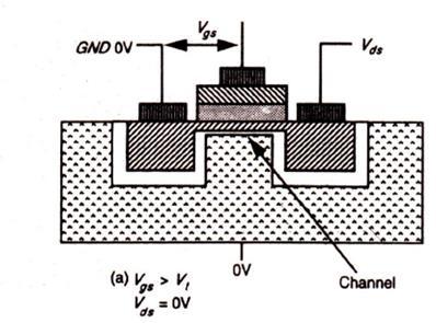
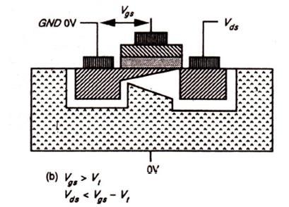
7 7

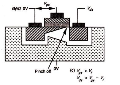
8 Let us now consider the situation when Vds is increased to a level greater than Vgs - Vt. In this case, an IR drop equal to Vgs Vt occurs over less than the whole length of the channel such that, near the drain, there is insufficient electric field available to give rise to an inversion layer to create the channel. The.channel is, therefore, 'pinched off as shown in Fig. (c). Diffusion current completes the path from source to drain in this case, causing the channel to exhibit a high resistance and behave as a constant current source. This region, known as saturation, is.characterized by almost constant current for increase of Vds above Vds = Vgs - Vt. In all cases, the channel will cease to exist and no current will flow when Vgs < Vt. Typically, for enhancement mode devices, Vt = 1 volt for VDD = 5 V or, in general terms, Vt = 0.2 VDD. DEPLETION MODE TRANSISTOR ACTION n-mos Depletion mode MOSFETs are built with P-type silicon substrates, and P- channel versions are built on N-type substrates. In both cases they include a thin gate oxide formed between the source and drain regions. A conductive channel is deliberately formed below the gate oxide layer and between the source and drain by using ion-implantation. By implanting the correct ion polarity in the channel region during fabrication determines the polarity of the threshold voltage (i.e. -Vt for an N channel transistor, or +Vt for an P-channel transistor). The actual concentration of ions in the substrate-to-channel region is used to adjust the threshold voltage (Vt) to the desired value. Depletion-mode devices are a little more difficult to manufacture and their characteristics harder to control than enhancement types, which do not require ion implantation. In depletion mode devices the channel is established, due to the implant, even when Vgs = 0, and to cause the channel to cease a negative voltage Vtd must be applied between gate and source. 8

9 Vtd is typically < VDD, depending on the implant and substrate bias, but, threshold voltage differences apart, the action is similar to that of the enhancement mode transistor. CMOS FABRICATION : CMOS fabrication is performed based on various methods, including the p-well, the n-well, the twin-tub, and the silicon-on-insulator processes.among these methods the p-well process is widely used in practice and the n-well process is also popular, particularly as it is an easy retrofit to existing nmos lines. (i) The p-well Process : The p-well structure consists of an n-type substrate in which p-devices may be formed by suitable masking and diffusion and, in order to accommodate n-type devices, a deep p-well is diffused into the n-type substrate as shown in the Fig.below. This diffusion should be carried out with special care since the p-well doping concentration and depth will affect the threshold voltages as well as the breakdown voltages of the n-transistors. To achieve low threshold voltages (0.6 to 1.0 V) either deep-well diffusion or high-well resistivity is required. However, deep wells require larger spacing between the n- and p-type transistors and wires due to lateral diffusion and therefore a larger chip area. The p-wells act as substrates for the n- devices within the parent n-substrate, and, the two areas are electrically isolated. Except this in all other respects- like masking, patterning, and diffusion-the process is similar to nmos fabrication. 9
 The diagram below")

10 p-well fabrication process(figs 1,2,3 & 4) The diagram below shows the CMOS p-well inverter showing VDD and Vss substrate connections 10

11 The n-well Process : Though the p-well process is widely used in C-MOS fabrication the n-well fabrication is also very popular because of the lower substrate bias effects on transistor threshold voltage and also lower parasitic capacitances associated with source and drain regions. The typical n-well fabrication steps are shown in the diagram below. Fig.n-well fabrication steps The first mask defines the n-well regions. This is followed by a low dose phosphorus implant driven in by a high temperature diffusion step to form the n-wells. The well depth is optimized to ensure against-substrate top+ diffusion breakdown without compromising then-well to n+ mask separation. The next steps are to define the devices and diffusion paths, grow field oxide, deposit and pattern the polysilicon, carry out the diffusions, make contact cuts, and finally metalize as before. lt will be seen that an n+ mask and its complement may be used to define the n- and p-diffusion regions respectively. These same masks also include the VDD and Vss contacts (respectively). It should be noted that, alternatively, we could have used a p+ mask and its complement since the n + and p + masks are generally complementary. The diagram below shows the Cross-sectional view of n-well CMOS Inverter. 11
, this is relatively unimportant since they contain a preponderance of n-channel devices.")

12 Due to the differences in charge carrier mobilities, the n-well process creates non-optimum p- channel characteristics. However, in many CMOS designs (such as domino-logic and dynamic logic structures), this is relatively unimportant since they contain a preponderance of n-channel devices. Thus then-channel transistors are mainly those used to form1ogic elements, providing speed and high density of elements. However, a factor of the n-well process is that the performance of the already poorly performing p-transistor is even further degraded. Modern process lines have come to grips with these problems, and good device performance may be achieved for both p-well and n-well fabrication. TWIN-TUB PROCESS Provide separate optimization of the n-type and p-type transistors This means that transistor parameters such as threshold voltage, body effect and the channel transconductance of both types of transistors can be tuned independently n+ or p+ substrate, with a lightly doped epitaxial layer on top, forms the starting material for this technology. The n-well and pwell are formed on this epitaxial layer which forms the actual substrate. The dopant concentrations can be carefully optimized to produce the desired device characteristics because two independent doping steps are performed to create the well regions. 12


13 BICMOS Technology : A BiCMOS circuit consist of both bipolar junction transistors and MOS transistors on a single substrate. The driving capability of MOS transistors is less because of limited current sourcing and sinking capabilities of the transistors. To drive large capacitive loads Bi-CMOS technology is used. As this technology combines Bipolar and CMOS transistors in a single integrated circuit, it has the advantages of both bipolar and CMOS transistors. BiCMOS is able to achieve VLSI circuits with speed-power-density performance previously not possible with either technology individually.the diagram given below shows the cross section of the BiCMOS process which uses an npn transistor Fig. Cross section of BiCMOS process The lay-out view of Bic-MOS transistor is shown in the figure below. The fabrication of BiCMOS is similar to CMOS but with certain additional process steps and additional masks are considered. They are (i) the p+ base region; (ii) n+ collector area; and (iii) the buried sub collector (BCCD). 13
14 BASIC ELECTRICAL PROPERTIES OF MOS Drain-to-Source Current IDS Versus Voltage VDS Relationships : The working of a MOS transistor is based on the principle that the use of a voltage on the gate induce a charge in the channel between source and drain, which may then be caused to move from source to drain under the influence of an electric field created by voltage Vds applied between drain and source. Since the charge induced is dependent on the gate to source voltage Vgs then Ids is dependent on both Vgs and Vds. Let us consider the diagram below in which electrons will flow source to drain.so,the drain current is given by Ids =-Isd = Charge induced in channel (Qc) Electron transit time(τ) Length of the channel Where the transit time is given by τsd = Velocity (v) 14

15 But velocity v= µeds Where µ =electron or hole mobility and also, Eds = Electric field Eds = Vds/L so, and τds = L 2 / µ.vds v = µ.vds/l The typical values of µ at room temperature are given below. The Non-saturated Region : Let us consider the Id vs Vd relationships in the non-saturated region.the charge induced in the channel due to due to the voltage difference between the gate and the channel, Vgs (assuming substrate connected to source). The voltage along the channel varies linearly with distance X from the source due to the IR drop in the channel.in the non-saturated state the average value is Vds/2. Also the effective gate voltage Vg = Vgs Vt where Vt, is the threshold voltage needed to invert the charge under the gate and establish the channel. Hence the induced charge is Q c = E g ε ins ε ow. L 15
16 where So, we can write that Eg = average electric field gate to channel εins = relative permittivity of insulation between gate and channel εo = permittivity of free space. Here D is the thickness of the oxide layer. Thus So, by combining the above two equations,we get or the above equation can be written as In the non-saturated or resistive region where Vds < Vgs Vt and Generally,a constant β is defined as So that,the expression for drain source current will become The gate /channel capacitance is 16
17 Hence we can write another alternative form forthe drain current as Some time it is also convenient to use gate capacitance per unit area,cg So,the drain current is This is the relation between drain current and drain-source voltage in non-saturated region. The Saturated Region Saturation begins when Vds = Vgs - V, since at this point the IR drop in the channel equals the effective gate to channel voltage at the drain and we may assume that the current remains fairly constant as Vds increases further. Thus or we can also write that or it can also be written as or The expressions derived above for Ids hold for both enhancement and depletion mode devices. Here the threshold voltage for the nmos depletion mode device (denoted as Vtd) is negative. 17
18 MOS Transistor Threshold Voltage Vt : The gate structure of a MOS transistor consists, of charges stored in the dielectric layers and in the surface to surface interfaces as well as in the substrate itself. Switching an enhancement mode MOS transistor from the off to the on state consists in applying sufficient gate voltage to neutralize these charges and enable the underlying silicon to undergo an inversion due to the electric field from the gate. Switching a depletion mode nmos transistor from the on to the off state consists in applying enough voltage to the gate to add to the stored charge and invert the 'n' implant region to 'p'. The threshold voltage Vt may be expressed as: where QD = the charge per unit area in the depletion layer below the oxide Qss = charge density at Si: SiO2 interface Co =Capacitance per unit area. Φns = work function difference between gate and Si ΦfN = Fermi level potential between inverted surface and bulk Si For polynomial gate and silicon substrate, the value of Φns is negative but negligible and the magnitude and sign of Vt are thus determined by balancing the other terms in the equation. To evaluate the Vt the other terms are determined as below. 18

19 Body Effect : Generally while studying the MOS transistors it is treated as a three terminal device. But,the body of the transistor is also an implicit terminal which helps to understand the characteristics of the transistor. Considering the body of the MOS transistor as a terminal is known as the body effect. The potential difference between the source and the body (Vsb) affects the threshold voltage of the transistor. In many situations, this Body Effect is relatively insignificant, so we can (unless otherwise stated) ignore the Body Effect. But it is not always insignificant, in some cases it can have a tremendous impact on MOSFET circuit performance. Body effect - nmos device Increasing Vsb causes the channel to be depleted of charge carriers and thus the threshold voltage is raised. Change in Vt is given by ΔVt = γ.(vsb) 1/2 where γ is a constant which depends on substrate doping so that the more lightly doped the substrate, the smaller will be the body effect The threshold voltage can be written as Where Vt(0) is the threshold voltage for Vsd = 0 19
20 For n-mos depletion mode transistors,the body voltage values at different VDD voltages are given below. VSB = 0 V ; Vsd = -0.7VDD (= V for VDD =+5V ) VSB = 5 V ; Vsd = -0.6VDD (= V for VDD =+5V ) 20
21 21
22 The nmos INVERTER : An inverter circuit is a very important circuit for producing a complete range of logic circuits. This is needed for restoring logic levels, for Nand and Nor gates, and for sequential and memory circuits of various forms. 22
23 A simple inverter circuit can be constructed using a transistor with source connected to ground and a load resistor of connected from the drain to the positive supply rail VDD The output is taken from the drain and the input applied between gate and ground. But, during the fabrication resistors are not conveniently produced on the silicon substrate and even small values of resistors occupy excessively large areas.hence some other form of load resistance is used. A more convenient way to solve this problem is to use a depletion mode transistor as the load, as shown in Fig. below. The salient features of the n-mos inverter are For the depletion mode transistor, the gate is connected to the source so it is always on. In this configuration the depletion mode device is called the pull-up (P.U) and the enhancement mode device the pull-down (P.D) transistor. With no current drawn from the output, the currents Ids for both transistors must be equal. nmos Inverter transfer characteristic. The transfer characteristic is drawn by taking Vds on x-axis and Ids on Y-axis for both enhancement and depletion mode transistors. So,to obtain the inverter transfer characteristic for 23
24 Vgs = 0 depletion mode characteristic curve is superimposed on the family of curves for the enhancement mode device and from the graph it can be seen that, maximum voltage across the enhancement mode device corresponds to minimum voltage across the depletion mode transistor. From the graph it is clear that as Vin(=Vgs p.d. transistor) exceeds the Pulldown threshold voltage current begins to flow. The output voltage Vout thus decreases and the subsequent increases in Vin will cause the Pull down transistor to come out of saturation and become resistive. During transition, the slope of transfer characteristics determine the gain Gain = Vout/ Vin 24
25 CMOS Inverter : 25
26 In region 2 the input voltage has increased to a level which just exceeds the threshold voltage of the n-transistor. The n-transistor conducts and has a large voltage between source and drain; so it is in saturation. The p-transistor is also conducting but with only a small voltage across it, it operates in the unsaturated resistive region. A small current now flows through the inverter from VDD to VSS. If we wish to analyze the behavior in this region, we equate the p-device resistive region current with the n-device saturation current and thus obtain the voltage and current relationships. Region 4 is similar to region 2 but with the roles of the p- and n-transistors reversed.however, the current magnitudes in regions 2 and 4 are small and most of the energy consumed in switching from one state to the other is due to the larger current which flows in region 3. 26
27 Region 3 is the region in which the inverter exhibits gain and in which both transistors are in saturation. The currents in each device must be the same,since the transistors are in series. So,we can write that Since both transistors are in saturation, they act as current sources so that the equivalent circuit in this region is two current sources in series between VDD and Vss with the output voltage coming from their common point. The region is inherently unstable in consequence and the changeover from one logic level to the other is rapid. Vin in terms of the β ratio and the other circuit voltages and currents Vin = VDD + Vtp +Vtn (βn + βp) 1/2 / 1+ (βn + βp) 1/2 Since both transistors are in saturation, they act as current sources so that the equivalent circuit in this region is two current sources so that the equivalent circuit in this region is two current sources in series between VDD and VSS with the output voltage coming from their common point. The region is inherently unstable in consequence and the change over from one logic level to the other is rapid. Since only at this point will the two β factors be equal. But for βn= βp the device geometries must be such that 27
28 µ pwp/lp = µ n Wn/Ln The motilities are inherently unequal and thus it is necessary for the width to length ratio of the p- device to be three times that of the n-device, namely Wp/Lp = 2.5 Wn/Ln The mobility µ is affected by the transverse electric field in the channel and is thus independent onvgs. It has been shown empirically that the actual mobility is µ= µ z (1 Ø (Vgs Vt) -1 Ø is a constant approximately equal to 0.05 Vt includes anybody effect, and µ z is the mobility with zero transverse field. ALTERNATIVE FORMS OF PULL UP Generally the inverter circuit will have a depletion mode pull-up transistor as its load. But there are also other configurations.let us consider four such arrangements. (i).load resistance RL : This arrangement consists of a load resistor as apull-up as shown in the diagram below.but it is not widely used because of the large space requirements of resistors produced in a silicon substrate. 28
29 2. nmos depletion mode transistor pull-up : This arrangement consists of a depletion mode transistor as pull-up. The arrangement and the transfer characteristic are shown below.in this type of arrangement we observe (a) Dissipation is high, since rail to rail current flows when Vin = logical 1. (b) Switching of output from 1 to 0 begins when Vin exceeds Vt, of pull-down device. nmos depletion mode transistor pull-up and transfer characteristic (c) When switching the output from 1 to 0, the pull-up device is non-saturated initially and this presents lower resistance through which to charge capacitive loads. 3. nmos enhancement mode pull-up :This arrangement consists of a n-mos enhancement mode transistor as pull-up. The arrangement and the transfer characteristic are shown below. 29
30 nmos enhancement mode pull-up and transfer characteristic The important features of this arrangement are (a) Dissipation is high since current flows when Vin =logical 1 (VGG is returned to VDD). (b) Vout can never reach VDD (logical I) if VGG = VDD as is normally the case. (c) VGG may be derived from a switching source, for example, one phase of a clock, so that dissipation can be greatly reduced. (d) If VGG is higher than VDD then an extra supply rail is required. 4. Complementary transistor pull-up (CMOS) : This arrangement consists of a C-MOS arrangement as pull-up. The arrangement and the transfer characteristic are shown below 30
 Full logical 1 and 0 levels are presented at the output.")
31 The salient features of this arrangement are (a) No current flows either for logical 0 or for logical 1 inputs. (b) Full logical 1 and 0 levels are presented at the output. (c) For devices of similar dimensions the p-channel is slower than the n-channel device. 31
32 32
33 33
Transistor was first invented by William.B.Shockley, Walter Brattain and John Bardeen of Bell Labratories. In 1961, first IC was introduced.
 Unit 1 Basic MOS Technology Transistor was first invented by William.B.Shockley, Walter Brattain and John Bardeen of Bell Labratories. In 1961, first IC was introduced. Levels of Integration:- i) SSI:-
INTRODUCTION TO MOS TECHNOLOGY
 INTRODUCTION TO MOS TECHNOLOGY 1. The MOS transistor The most basic element in the design of a large scale integrated circuit is the transistor. For the processes we will discuss, the type of transistor
Lecture Integrated circuits era
 Lecture 1 1.1 Integrated circuits era Transistor was first invented by William.B.Shockley, Walter Brattain and John Bardeen of Bell laboratories. In 1961, first IC was introduced. Levels of Integration:-
VBIT COURSE MATERIAL VLSI DESIGN
 VBIT COURSE MATERIAL VLSI DESIGN UNIT I INTRODUCTION: Introduction to IC Technology MOS, PMOS, NMOS, CMOS & BiCMOS technologies. VLSI DESIGN BASIC ELECTRICAL PROPERTIES : Basic Electrical Properties of
Design cycle for MEMS
 Design cycle for MEMS Design cycle for ICs IC Process Selection nmos CMOS BiCMOS ECL for logic for I/O and driver circuit for critical high speed parts of the system The Real Estate of a Wafer MOS Transistor
UNIT 3: FIELD EFFECT TRANSISTORS
 FIELD EFFECT TRANSISTOR: UNIT 3: FIELD EFFECT TRANSISTORS The field effect transistor is a semiconductor device, which depends for its operation on the control of current by an electric field. There are
INTRODUCTION: Basic operating principle of a MOSFET:
 INTRODUCTION: Along with the Junction Field Effect Transistor (JFET), there is another type of Field Effect Transistor available whose Gate input is electrically insulated from the main current carrying
Semiconductor Physics and Devices
 Metal-Semiconductor and Semiconductor Heterojunctions The Metal-Oxide-Semiconductor Field-Effect Transistor (MOSFET) is one of two major types of transistors. The MOSFET is used in digital circuit, because
Basic Fabrication Steps
 Basic Fabrication Steps and Layout Somayyeh Koohi Department of Computer Engineering Adapted with modifications from lecture notes prepared by author Outline Fabrication steps Transistor structures Transistor
MOS TRANSISTOR THEORY
 MOS TRANSISTOR THEORY Introduction A MOS transistor is a majority-carrier device, in which the current in a conducting channel between the source and the drain is modulated by a voltage applied to the
MOSFET & IC Basics - GATE Problems (Part - I)
") MOSFET & IC Basics - GATE Problems (Part - I) 1. Channel current is reduced on application of a more positive voltage to the GATE of the depletion mode n channel MOSFET. (True/False) [GATE 1994: 1 Mark]
MOSFET & IC Basics - GATE Problems (Part - I) 1. Channel current is reduced on application of a more positive voltage to the GATE of the depletion mode n channel MOSFET. (True/False) [GATE 1994: 1 Mark]
Three Terminal Devices
 Three Terminal Devices - field effect transistor (FET) - bipolar junction transistor (BJT) - foundation on which modern electronics is built - active devices - devices described completely by considering
Notes. (Subject Code: 7EC5)
") COMPUCOM INSTITUTE OF TECHNOLOGY & MANAGEMENT, JAIPUR (DEPARTMENT OF ELECTRONICS & COMMUNICATION) Notes VLSI DESIGN NOTES (Subject Code: 7EC5) Prepared By: MANVENDRA SINGH Class: B. Tech. IV Year, VII
COMPUCOM INSTITUTE OF TECHNOLOGY & MANAGEMENT, JAIPUR (DEPARTMENT OF ELECTRONICS & COMMUNICATION) Notes VLSI DESIGN NOTES (Subject Code: 7EC5) Prepared By: MANVENDRA SINGH Class: B. Tech. IV Year, VII
4.1 Device Structure and Physical Operation
 10/12/2004 4_1 Device Structure and Physical Operation blank.doc 1/2 4.1 Device Structure and Physical Operation Reading Assignment: pp. 235-248 Chapter 4 covers Field Effect Transistors ( ) Specifically,
EE301 Electronics I , Fall
 EE301 Electronics I 2018-2019, Fall 1. Introduction to Microelectronics (1 Week/3 Hrs.) Introduction, Historical Background, Basic Consepts 2. Rewiev of Semiconductors (1 Week/3 Hrs.) Semiconductor materials
Fundamentals of CMOS VLSI PART-A
 Fundamentals of CMOS VLSI Subject Code: Semester: V PART-A Unit 1: Basic MOS Technology Integrated circuits era, enhancement and depletion mode MOS transistors. nmos fabrication. CMOS fabrication, Thermal
MEASUREMENT AND INSTRUMENTATION STUDY NOTES UNIT-I
 MEASUREMENT AND INSTRUMENTATION STUDY NOTES The MOSFET The MOSFET Metal Oxide FET UNIT-I As well as the Junction Field Effect Transistor (JFET), there is another type of Field Effect Transistor available
Solid State Devices- Part- II. Module- IV
 Solid State Devices- Part- II Module- IV MOS Capacitor Two terminal MOS device MOS = Metal- Oxide- Semiconductor MOS capacitor - the heart of the MOSFET The MOS capacitor is used to induce charge at the
VLSI Design. Introduction
 VLSI Design Introduction Outline Introduction Silicon, pn-junctions and transistors A Brief History Operation of MOS Transistors CMOS circuits Fabrication steps for CMOS circuits Introduction Integrated
Lecture 4. MOS transistor theory
 Lecture 4 MOS transistor theory 1.7 Introduction: A MOS transistor is a majority-carrier device, in which the current in a conducting channel between the source and the drain is modulated by a voltage
420 Intro to VLSI Design
 Dept of Electrical and Computer Engineering 420 Intro to VLSI Design Lecture 0: Course Introduction and Overview Valencia M. Joyner Spring 2005 Getting Started Syllabus About the Instructor Labs, Problem
Student Lecture by: Giangiacomo Groppi Joel Cassell Pierre Berthelot September 28 th 2004
 Student Lecture by: Giangiacomo Groppi Joel Cassell Pierre Berthelot September 28 th 2004 Lecture outline Historical introduction Semiconductor devices overview Bipolar Junction Transistor (BJT) Field
UNIT-VI FIELD EFFECT TRANSISTOR. 1. Explain about the Field Effect Transistor and also mention types of FET s.
 UNIT-I FIELD EFFECT TRANSISTOR 1. Explain about the Field Effect Transistor and also mention types of FET s. The Field Effect Transistor, or simply FET however, uses the voltage that is applied to their
Module-3: Metal Oxide Semiconductor (MOS) & Emitter coupled logic (ECL) families
 & Emitter coupled logic (ECL) families") 1 Module-3: Metal Oxide Semiconductor (MOS) & Emitter coupled logic (ECL) families 1. Introduction 2. Metal Oxide Semiconductor (MOS) logic 2.1. Enhancement and depletion mode 2.2. NMOS and PMOS inverter
1 Module-3: Metal Oxide Semiconductor (MOS) & Emitter coupled logic (ECL) families 1. Introduction 2. Metal Oxide Semiconductor (MOS) logic 2.1. Enhancement and depletion mode 2.2. NMOS and PMOS inverter
Digital Electronics. By: FARHAD FARADJI, Ph.D. Assistant Professor, Electrical and Computer Engineering, K. N. Toosi University of Technology
 K. N. Toosi University of Technology Chapter 7. Field-Effect Transistors By: FARHAD FARADJI, Ph.D. Assistant Professor, Electrical and Computer Engineering, K. N. Toosi University of Technology http://wp.kntu.ac.ir/faradji/digitalelectronics.htm
EMT 251 Introduction to IC Design
 EMT 251 Introduction to IC Design (Pengantar Rekabentuk Litar Terkamir) Semester II 2011/2012 Introduction to IC design and Transistor Fundamental Some Keywords! Very-large-scale-integration (VLSI) is
Conduction Characteristics of MOS Transistors (for fixed Vds)! Topic 2. Basic MOS theory & SPICE simulation. MOS Transistor
! Topic 2. Basic MOS theory & SPICE simulation. MOS Transistor") Conduction Characteristics of MOS Transistors (for fixed Vds)! Topic 2 Basic MOS theory & SPICE simulation Peter Cheung Department of Electrical & Electronic Engineering Imperial College London (Weste&Harris,
Conduction Characteristics of MOS Transistors (for fixed Vds)! Topic 2 Basic MOS theory & SPICE simulation Peter Cheung Department of Electrical & Electronic Engineering Imperial College London (Weste&Harris,
Topic 2. Basic MOS theory & SPICE simulation
 Topic 2 Basic MOS theory & SPICE simulation Peter Cheung Department of Electrical & Electronic Engineering Imperial College London (Weste&Harris, Ch 2 & 5.1-5.3 Rabaey, Ch 3) URL: www.ee.ic.ac.uk/pcheung/
Conduction Characteristics of MOS Transistors (for fixed Vds) Topic 2. Basic MOS theory & SPICE simulation. MOS Transistor
 Topic 2. Basic MOS theory & SPICE simulation. MOS Transistor") Conduction Characteristics of MOS Transistors (for fixed Vds) Topic 2 Basic MOS theory & SPICE simulation Peter Cheung Department of Electrical & Electronic Engineering Imperial College London (Weste&Harris,
Conduction Characteristics of MOS Transistors (for fixed Vds) Topic 2 Basic MOS theory & SPICE simulation Peter Cheung Department of Electrical & Electronic Engineering Imperial College London (Weste&Harris,
FET. Field Effect Transistors ELEKTRONIKA KONTROL. Eka Maulana, ST, MT, M.Eng. Universitas Brawijaya. p + S n n-channel. Gate. Basic structure.
 FET Field Effect Transistors ELEKTRONIKA KONTROL Basic structure Gate G Source S n n-channel Cross section p + p + p + G Depletion region Drain D Eka Maulana, ST, MT, M.Eng. Universitas Brawijaya S Channel
VLSI Design. Introduction
 Tassadaq Hussain VLSI Design Introduction Outcome of this course Problem Aims Objectives Outcomes Data Collection Theoretical Model Mathematical Model Validate Development Analysis and Observation Pseudo
ECE 340 Lecture 40 : MOSFET I
 ECE 340 Lecture 40 : MOSFET I Class Outline: MOS Capacitance-Voltage Analysis MOSFET - Output Characteristics MOSFET - Transfer Characteristics Things you should know when you leave Key Questions How do
ECE520 VLSI Design. Lecture 2: Basic MOS Physics. Payman Zarkesh-Ha
 ECE520 VLSI Design Lecture 2: Basic MOS Physics Payman Zarkesh-Ha Office: ECE Bldg. 230B Office hours: Wednesday 2:00-3:00PM or by appointment E-mail: pzarkesh@unm.edu Slide: 1 Review of Last Lecture Semiconductor
PAPER SOLUTION_DECEMBER_2014_VLSI_DESIGN_ETRX_SEM_VII Prepared by Girish Gidaye
 Q1a) The MOS System under External Bias Depending on the polarity and the magnitude of V G, three different operating regions can be observed for the MOS system: 1) Accumulation 2) Depletion 3) Inversion
FIELD EFFECT TRANSISTORS MADE BY : GROUP (13)/PM
/PM") FIELD EFFECT TRANSISTORS MADE BY : GROUP (13)/PM THE FIELD EFFECT TRANSISTOR (FET) In 1945, Shockley had an idea for making a solid state device out of semiconductors. He reasoned that a strong electrical
FIELD EFFECT TRANSISTORS MADE BY : GROUP (13)/PM THE FIELD EFFECT TRANSISTOR (FET) In 1945, Shockley had an idea for making a solid state device out of semiconductors. He reasoned that a strong electrical
MOSFET Terminals. The voltage applied to the GATE terminal determines whether current can flow between the SOURCE & DRAIN terminals.
 MOSFET Terminals The voltage applied to the GATE terminal determines whether current can flow between the SOURCE & DRAIN terminals. For an n-channel MOSFET, the SOURCE is biased at a lower potential (often
UNIT I CMOS TECHNOLOGY
 DEPARTMENT: ECE SUBJECT NAME: VLSI DESIGN QUESTION BANK SEMESTER VI SUBJECT CODE: EC2354 UNIT I CMOS TECHNOLOGY PART A ( 2 MARKS) 1. What are four generations of Integration Circuits? SSI (Small Scale
Field Effect Transistors (FET s) University of Connecticut 136
 University of Connecticut 136") Field Effect Transistors (FET s) University of Connecticut 136 Field Effect Transistors (FET s) FET s are classified three ways: by conduction type n-channel - conduction by electrons p-channel - conduction
Field Effect Transistors (FET s) University of Connecticut 136 Field Effect Transistors (FET s) FET s are classified three ways: by conduction type n-channel - conduction by electrons p-channel - conduction
Laboratory #5 BJT Basics and MOSFET Basics
 Laboratory #5 BJT Basics and MOSFET Basics I. Objectives 1. Understand the physical structure of BJTs and MOSFETs. 2. Learn to measure I-V characteristics of BJTs and MOSFETs. II. Components and Instruments
FIELD EFFECT TRANSISTOR (FET) 1. JUNCTION FIELD EFFECT TRANSISTOR (JFET)
 1. JUNCTION FIELD EFFECT TRANSISTOR (JFET)") FIELD EFFECT TRANSISTOR (FET) The field-effect transistor (FET) is a three-terminal device used for a variety of applications that match, to a large extent, those of the BJT transistor. Although there
FIELD EFFECT TRANSISTOR (FET) The field-effect transistor (FET) is a three-terminal device used for a variety of applications that match, to a large extent, those of the BJT transistor. Although there
Field-Effect Transistor (FET) is one of the two major transistors; FET derives its name from its working mechanism;
 is one of the two major transistors; FET derives its name from its working mechanism;") Chapter 3 Field-Effect Transistors (FETs) 3.1 Introduction Field-Effect Transistor (FET) is one of the two major transistors; FET derives its name from its working mechanism; The concept has been known
Chapter 3 Field-Effect Transistors (FETs) 3.1 Introduction Field-Effect Transistor (FET) is one of the two major transistors; FET derives its name from its working mechanism; The concept has been known
(Refer Slide Time: 02:05)
") Electronics for Analog Signal Processing - I Prof. K. Radhakrishna Rao Department of Electrical Engineering Indian Institute of Technology Madras Lecture 27 Construction of a MOSFET (Refer Slide Time:
Electronics for Analog Signal Processing - I Prof. K. Radhakrishna Rao Department of Electrical Engineering Indian Institute of Technology Madras Lecture 27 Construction of a MOSFET (Refer Slide Time:
8. Characteristics of Field Effect Transistor (MOSFET)
") 1 8. Characteristics of Field Effect Transistor (MOSFET) 8.1. Objectives The purpose of this experiment is to measure input and output characteristics of n-channel and p- channel field effect transistors
1 8. Characteristics of Field Effect Transistor (MOSFET) 8.1. Objectives The purpose of this experiment is to measure input and output characteristics of n-channel and p- channel field effect transistors
55:041 Electronic Circuits
 55:041 Electronic Circuits Mosfet Review Sections of Chapter 3 &4 A. Kruger Mosfet Review, Page-1 Basic Structure of MOS Capacitor Sect. 3.1 Width 1 10-6 m or less Thickness 50 10-9 m or less ` MOS Metal-Oxide-Semiconductor
UNIT-1 Bipolar Junction Transistors. Text Book:, Microelectronic Circuits 6 ed., by Sedra and Smith, Oxford Press
 UNIT-1 Bipolar Junction Transistors Text Book:, Microelectronic Circuits 6 ed., by Sedra and Smith, Oxford Press Figure 6.1 A simplified structure of the npn transistor. Microelectronic Circuits, Sixth
FUNDAMENTALS OF MODERN VLSI DEVICES
 19-13- FUNDAMENTALS OF MODERN VLSI DEVICES YUAN TAUR TAK H. MING CAMBRIDGE UNIVERSITY PRESS Physical Constants and Unit Conversions List of Symbols Preface page xi xiii xxi 1 INTRODUCTION I 1.1 Evolution
Sub-Threshold Region Behavior of Long Channel MOSFET
 Sub-threshold Region - So far, we have discussed the MOSFET behavior in linear region and saturation region - Sub-threshold region is refer to region where Vt is less than Vt - Sub-threshold region reflects
VLSI Technology Dr. Nandita Dasgupta Department of Electrical Engineering Indian Institute of Technology, Madras
 VLSI Technology Dr. Nandita Dasgupta Department of Electrical Engineering Indian Institute of Technology, Madras Lecture - 39 Latch up in CMOS We have been discussing about the problems in CMOS, basic
Department of Electrical Engineering IIT Madras
 Department of Electrical Engineering IIT Madras Sample Questions on Semiconductor Devices EE3 applicants who are interested to pursue their research in microelectronics devices area (fabrication and/or
ECE 340 Lecture 37 : Metal- Insulator-Semiconductor FET Class Outline:
 ECE 340 Lecture 37 : Metal- Insulator-Semiconductor FET Class Outline: Metal-Semiconductor Junctions MOSFET Basic Operation MOS Capacitor Things you should know when you leave Key Questions What is the
Field-Effect Transistors
 R L 2 Field-Effect Transistors 2.1 BAIC PRINCIPLE OF JFET The eld-effect transistor (FET) is an electric- eld (voltage) operated transistor, developed as a semiconductor equivalent of the vacuum-tube device,
Introduction to VLSI ASIC Design and Technology
 Introduction to VLSI ASIC Design and Technology Paulo Moreira CERN - Geneva, Switzerland Paulo Moreira Introduction 1 Outline Introduction Is there a limit? Transistors CMOS building blocks Parasitics
UNIT-1 Fundamentals of Low Power VLSI Design
 UNIT-1 Fundamentals of Low Power VLSI Design Need for Low Power Circuit Design: The increasing prominence of portable systems and the need to limit power consumption (and hence, heat dissipation) in very-high
An introduction to Depletion-mode MOSFETs By Linden Harrison
 An introduction to Depletion-mode MOSFETs By Linden Harrison Since the mid-nineteen seventies the enhancement-mode MOSFET has been the subject of almost continuous global research, development, and refinement
Integrated diodes. The forward voltage drop only slightly depends on the forward current. ELEKTRONIKOS ĮTAISAI
 1 Integrated diodes pn junctions of transistor structures can be used as integrated diodes. The choice of the junction is limited by the considerations of switching speed and breakdown voltage. The forward
EE 5611 Introduction to Microelectronic Technologies Fall Thursday, September 04, 2014 Lecture 02
 EE 5611 Introduction to Microelectronic Technologies Fall 2014 Thursday, September 04, 2014 Lecture 02 1 Lecture Outline Review on semiconductor materials Review on microelectronic devices Example of microelectronic
TECHNO INDIA BATANAGAR (DEPARTMENT OF ELECTRONICS & COMMUNICATION ENGINEERING) QUESTION BANK- 2018
 QUESTION BANK- 2018") TECHNO INDIA BATANAGAR (DEPARTMENT OF ELECTRONICS & COMMUNICATION ENGINEERING) QUESTION BANK- 2018 Paper Setter Detail Name Designation Mobile No. E-mail ID Raina Modak Assistant Professor 6290025725 raina.modak@tib.edu.in
TECHNO INDIA BATANAGAR (DEPARTMENT OF ELECTRONICS & COMMUNICATION ENGINEERING) QUESTION BANK- 2018 Paper Setter Detail Name Designation Mobile No. E-mail ID Raina Modak Assistant Professor 6290025725 raina.modak@tib.edu.in
MOS Field-Effect Transistors (MOSFETs)
") 6 MOS Field-Effect Transistors (MOSFETs) A three-terminal device that uses the voltages of the two terminals to control the current flowing in the third terminal. The basis for amplifier design. The basis
6 MOS Field-Effect Transistors (MOSFETs) A three-terminal device that uses the voltages of the two terminals to control the current flowing in the third terminal. The basis for amplifier design. The basis
EC0306 INTRODUCTION TO VLSI DESIGN
 EC0306 INTRODUCTION TO VLSI DESIGN UNIT I INTRODUCTION TO MOS CIRCUITS Why VLSI? Integration improves the design: o lower parasitics = higher speed; o lower power; o physically smaller. Integration reduces
AE53/AC53/AT53/AE103 ELECT. DEVICES & CIRCUITS DEC 2015
 Q.2 a. By using Norton s theorem, find the current in the load resistor R L for the circuit shown in Fig.1. (8) Fig.1 IETE 1 b. Explain Z parameters and also draw an equivalent circuit of the Z parameter
Solid State Device Fundamentals
 Solid State Device Fundamentals 4.4. Field Effect Transistor (MOSFET) ENS 463 Lecture Course by Alexander M. Zaitsev alexander.zaitsev@csi.cuny.edu Tel: 718 982 2812 4N101b 1 Field-effect transistor (FET)
Learning Outcomes. Spiral 2-6. Current, Voltage, & Resistors DIODES
 26.1 26.2 Learning Outcomes Spiral 26 Semiconductor Material MOS Theory I underst why a diode conducts current under forward bias but does not under reverse bias I underst the three modes of operation
In this lecture we will begin a new topic namely the Metal-Oxide-Semiconductor Field Effect Transistor.
 Solid State Devices Dr. S. Karmalkar Department of Electronics and Communication Engineering Indian Institute of Technology, Madras Lecture - 38 MOS Field Effect Transistor In this lecture we will begin
Depletion-mode operation ( 공핍형 ): Using an input gate voltage to effectively decrease the channel size of an FET
: Using an input gate voltage to effectively decrease the channel size of an FET") Ch. 13 MOSFET Metal-Oxide-Semiconductor Field-Effect Transistor : I D D-mode E-mode V g The gate oxide is made of dielectric SiO 2 with e = 3.9 Depletion-mode operation ( 공핍형 ): Using an input gate voltage
Ch. 13 MOSFET Metal-Oxide-Semiconductor Field-Effect Transistor : I D D-mode E-mode V g The gate oxide is made of dielectric SiO 2 with e = 3.9 Depletion-mode operation ( 공핍형 ): Using an input gate voltage
BICMOS Technology and Fabrication
 12-1 BICMOS Technology and Fabrication 12-2 Combines Bipolar and CMOS transistors in a single integrated circuit By retaining benefits of bipolar and CMOS, BiCMOS is able to achieve VLSI circuits with
MODULE-2: Field Effect Transistors (FET)
") FORMAT-1B Definition: MODULE-2: Field Effect Transistors (FET) FET is a three terminal electronic device used for variety of applications that match with BJT. In FET, an electric field is established by
FORMAT-1B Definition: MODULE-2: Field Effect Transistors (FET) FET is a three terminal electronic device used for variety of applications that match with BJT. In FET, an electric field is established by
Design Simulation and Analysis of NMOS Characteristics for Varying Oxide Thickness
 MIT International Journal of Electronics and Communication Engineering, Vol. 4, No. 2, August 2014, pp. 81 85 81 Design Simulation and Analysis of NMOS Characteristics for Varying Oxide Thickness Alpana
EE70 - Intro. Electronics
 EE70 - Intro. Electronics Course website: ~/classes/ee70/fall05 Today s class agenda (November 28, 2005) review Serial/parallel resonant circuits Diode Field Effect Transistor (FET) f 0 = Qs = Qs = 1 2π
Architecture of Computers and Parallel Systems Part 9: Digital Circuits
 Architecture of Computers and Parallel Systems Part 9: Digital Circuits Ing. Petr Olivka petr.olivka@vsb.cz Department of Computer Science FEI VSB-TUO Architecture of Computers and Parallel Systems Part
55:041 Electronic Circuits
 55:041 Electronic Circuits MOSFETs Sections of Chapter 3 &4 A. Kruger MOSFETs, Page-1 Basic Structure of MOS Capacitor Sect. 3.1 Width = 1 10-6 m or less Thickness = 50 10-9 m or less ` MOS Metal-Oxide-Semiconductor
EE105 Fall 2015 Microelectronic Devices and Circuits: MOSFET Prof. Ming C. Wu 511 Sutardja Dai Hall (SDH)
") EE105 Fall 2015 Microelectronic Devices and Circuits: MOSFET Prof. Ming C. Wu wu@eecs.berkeley.edu 511 Sutardja Dai Hall (SDH) 7-1 Simplest Model of MOSFET (from EE16B) 7-2 CMOS Inverter 7-3 CMOS NAND
EE105 Fall 2015 Microelectronic Devices and Circuits: MOSFET Prof. Ming C. Wu wu@eecs.berkeley.edu 511 Sutardja Dai Hall (SDH) 7-1 Simplest Model of MOSFET (from EE16B) 7-2 CMOS Inverter 7-3 CMOS NAND
ECE 5745 Complex Digital ASIC Design Topic 2: CMOS Devices
 ECE 5745 Complex Digital ASIC Design Topic 2: CMOS Devices Christopher Batten School of Electrical and Computer Engineering Cornell University http://www.csl.cornell.edu/courses/ece5950 Simple Transistor
Review Energy Bands Carrier Density & Mobility Carrier Transport Generation and Recombination
 Review Energy Bands Carrier Density & Mobility Carrier Transport Generation and Recombination Current Transport: Diffusion, Thermionic Emission & Tunneling For Diffusion current, the depletion layer is
Lecture 020 ECE4430 Review II (1/5/04) Page 020-1
 Page 020-1") Lecture 020 ECE4430 Review II (1/5/04) Page 020-1 LECTURE 020 ECE 4430 REVIEW II (READING: GHLM - Chap. 2) Objective The objective of this presentation is: 1.) Identify the prerequisite material as taught
Lecture 020 ECE4430 Review II (1/5/04) Page 020-1 LECTURE 020 ECE 4430 REVIEW II (READING: GHLM - Chap. 2) Objective The objective of this presentation is: 1.) Identify the prerequisite material as taught
UNIT III VLSI CIRCUIT DESIGN PROCESSES. In this chapter we will be studying how to get the schematic into stick diagrams or layouts.
 UNIT III VLSI CIRCUIT DESIGN PROCESSES In this chapter we will be studying how to get the schematic into stick diagrams or layouts. MOS circuits are formed on four basic layers: N-diffusion P-diffusion
Lecture 020 ECE4430 Review II (1/5/04) Page 020-1
 Page 020-1") Lecture 020 ECE4430 Review II (1/5/04) Page 020-1 LECTURE 020 ECE 4430 REVIEW II (READING: GHLM - Chap. 2) Objective The objective of this presentation is: 1.) Identify the prerequisite material as taught
Lecture 020 ECE4430 Review II (1/5/04) Page 020-1 LECTURE 020 ECE 4430 REVIEW II (READING: GHLM - Chap. 2) Objective The objective of this presentation is: 1.) Identify the prerequisite material as taught
EE 42/100 Lecture 23: CMOS Transistors and Logic Gates. Rev A 4/15/2012 (10:39 AM) Prof. Ali M. Niknejad
 Prof. Ali M. Niknejad") A. M. Niknejad University of California, Berkeley EE 100 / 42 Lecture 23 p. 1/16 EE 42/100 Lecture 23: CMOS Transistors and Logic Gates ELECTRONICS Rev A 4/15/2012 (10:39 AM) Prof. Ali M. Niknejad University
A. M. Niknejad University of California, Berkeley EE 100 / 42 Lecture 23 p. 1/16 EE 42/100 Lecture 23: CMOS Transistors and Logic Gates ELECTRONICS Rev A 4/15/2012 (10:39 AM) Prof. Ali M. Niknejad University
+1 (479)
") Introduction to VLSI Design http://csce.uark.edu +1 (479) 575-6043 yrpeng@uark.edu Invention of the Transistor Vacuum tubes ruled in first half of 20th century Large, expensive, power-hungry, unreliable
Introduction to VLSI Design http://csce.uark.edu +1 (479) 575-6043 yrpeng@uark.edu Invention of the Transistor Vacuum tubes ruled in first half of 20th century Large, expensive, power-hungry, unreliable
FET(Field Effect Transistor)
") Field Effect Transistor: Construction and Characteristic of JFETs. Transfer Characteristic. CS,CD,CG amplifier and analysis of CS amplifier MOSFET (Depletion and Enhancement) Type, Transfer Characteristic,
Field Effect Transistor: Construction and Characteristic of JFETs. Transfer Characteristic. CS,CD,CG amplifier and analysis of CS amplifier MOSFET (Depletion and Enhancement) Type, Transfer Characteristic,
UNIT 3 Transistors JFET
 UNIT 3 Transistors JFET Mosfet Definition of BJT A bipolar junction transistor is a three terminal semiconductor device consisting of two p-n junctions which is able to amplify or magnify a signal. It
Fin-Shaped Field Effect Transistor (FinFET) Min Ku Kim 03/07/2018
 Min Ku Kim 03/07/2018") Fin-Shaped Field Effect Transistor (FinFET) Min Ku Kim 03/07/2018 ECE 658 Sp 2018 Semiconductor Materials and Device Characterizations OUTLINE Background FinFET Future Roadmap Keeping up w/ Moore s Law
Fin-Shaped Field Effect Transistor (FinFET) Min Ku Kim 03/07/2018 ECE 658 Sp 2018 Semiconductor Materials and Device Characterizations OUTLINE Background FinFET Future Roadmap Keeping up w/ Moore s Law
SRM INSTITUTE OF SCIENCE AND TECHNOLOGY (DEEMED UNIVERSITY)
") SRM INSTITUTE OF SCIENCE AND TECHNOLOGY (DEEMED UNIVERSITY) QUESTION BANK I YEAR B.Tech (II Semester) ELECTRONIC DEVICES (COMMON FOR EC102, EE104, IC108, BM106) UNIT-I PART-A 1. What are intrinsic and
SRM INSTITUTE OF SCIENCE AND TECHNOLOGY (DEEMED UNIVERSITY) QUESTION BANK I YEAR B.Tech (II Semester) ELECTRONIC DEVICES (COMMON FOR EC102, EE104, IC108, BM106) UNIT-I PART-A 1. What are intrinsic and
NAME: Last First Signature
 UNIVERSITY OF CALIFORNIA, BERKELEY College of Engineering Department of Electrical Engineering and Computer Sciences EE 130: IC Devices Spring 2003 FINAL EXAMINATION NAME: Last First Signature STUDENT
Session 10: Solid State Physics MOSFET
 Session 10: Solid State Physics MOSFET 1 Outline A B C D E F G H I J 2 MOSCap MOSFET Metal-Oxide-Semiconductor Field-Effect Transistor: Al (metal) SiO2 (oxide) High k ~0.1 ~5 A SiO2 A n+ n+ p-type Si (bulk)
Organic Electronics. Information: Information: 0331a/ 0442/
 Organic Electronics (Course Number 300442 ) Spring 2006 Organic Field Effect Transistors Instructor: Dr. Dietmar Knipp Information: Information: http://www.faculty.iubremen.de/course/c30 http://www.faculty.iubremen.de/course/c30
CMOS Technology. 1. Why CMOS 2. Qualitative MOSFET model 3. Building a MOSFET 4. CMOS logic gates. Handouts: Lecture Slides. metal ndiff.
 CMOS Technology 1. Why CMOS 2. Qualitative MOSFET model 3. Building a MOSFET 4. CMOS logic gates poly pdiff metal ndiff Handouts: Lecture Slides L03 - CMOS Technology 1 Building Bits from Atoms V in V
INTERNATIONAL JOURNAL OF APPLIED ENGINEERING RESEARCH, DINDIGUL Volume 1, No 3, 2010
 Low Power CMOS Inverter design at different Technologies Vijay Kumar Sharma 1, Surender Soni 2 1 Department of Electronics & Communication, College of Engineering, Teerthanker Mahaveer University, Moradabad
problem grade total
 Fall 2005 6.012 Microelectronic Devices and Circuits Prof. J. A. del Alamo Name: Recitation: November 16, 2005 Quiz #2 problem grade 1 2 3 4 total General guidelines (please read carefully before starting):
COLLECTOR DRAIN BASE GATE EMITTER. Applying a voltage to the Gate connection allows current to flow between the Drain and Source connections.
 MOSFETS Although the base current in a transistor is usually small (< 0.1 ma), some input devices (e.g. a crystal microphone) may be limited in their output. In order to overcome this, a Field Effect Transistor
Chapter 2 : Semiconductor Materials & Devices (II) Feb
 Feb") Chapter 2 : Semiconductor Materials & Devices (II) 1 Reference 1. SemiconductorManufacturing Technology: Michael Quirk and Julian Serda (2001) 3. Microelectronic Circuits (5/e): Sedra & Smith (2004) 4.
Chapter 2 : Semiconductor Materials & Devices (II) 1 Reference 1. SemiconductorManufacturing Technology: Michael Quirk and Julian Serda (2001) 3. Microelectronic Circuits (5/e): Sedra & Smith (2004) 4.
EE4800 CMOS Digital IC Design & Analysis. Lecture 1 Introduction Zhuo Feng
 EE4800 CMOS Digital IC Design & Analysis Lecture 1 Introduction Zhuo Feng 1.1 Prof. Zhuo Feng Office: EERC 730 Phone: 487-3116 Email: zhuofeng@mtu.edu Class Website http://www.ece.mtu.edu/~zhuofeng/ee4800fall2010.html
Lecture 0: Introduction
 Lecture 0: Introduction Introduction Integrated circuits: many transistors on one chip. Very Large Scale Integration (VLSI): bucketloads! Complementary Metal Oxide Semiconductor Fast, cheap, low power
Integrated Circuits: FABRICATION & CHARACTERISTICS - 4. Riju C Issac
 Integrated Circuits: FABRICATION & CHARACTERISTICS - 4 Riju C Issac INTEGRATED RESISTORS Resistor in a monolithic IC is very often obtained by the bulk resistivity of one of the diffused areas. P-type
BASIC PHYSICAL DESIGN AN OVERVIEW The VLSI design flow for any IC design is as follows
 Unit 3 BASIC PHYSICAL DESIGN AN OVERVIEW The VLSI design flow for any IC design is as follows 1.Specification (problem definition) 2.Schematic(gate level design) (equivalence check) 3.Layout (equivalence
The Design and Realization of Basic nmos Digital Devices
 Proceedings of The National Conference On Undergraduate Research (NCUR) 2004 Indiana University Purdue University Indianapolis, Indiana April 15-17, 2004 The Design and Realization of Basic nmos Digital
Mechanis m Faliures. Group Leader Jepsy 1)Substrate Biasing 2) Minority Injection. Bob 1)Minority-Carrier Guard Rings
Substrate Biasing 2) Minority Injection. Bob 1)Minority-Carrier Guard Rings") Mechanis m Faliures Group Leader Jepsy 1)Substrate Biasing 2) Minority Injection As im 1)Types Of Guard Rings Sandra 1)Parasitics 2)Field Plating Bob 1)Minority-Carrier Guard Rings Shawn 1)Parasitic Channel
Mechanis m Faliures Group Leader Jepsy 1)Substrate Biasing 2) Minority Injection As im 1)Types Of Guard Rings Sandra 1)Parasitics 2)Field Plating Bob 1)Minority-Carrier Guard Rings Shawn 1)Parasitic Channel
Chapter 3: Basics Semiconductor Devices and Processing 2006/9/27 1. Topics
 Chapter 3: Basics Semiconductor Devices and Processing 2006/9/27 1 Topics What is semiconductor Basic semiconductor devices Basics of IC processing CMOS technologies 2006/9/27 2 1 What is Semiconductor
Unit III FET and its Applications. 2 Marks Questions and Answers
 Unit III FET and its Applications 2 Marks Questions and Answers 1. Why do you call FET as field effect transistor? The name field effect is derived from the fact that the current is controlled by an electric
UNIT-II LOW POWER VLSI DESIGN APPROACHES
 UNIT-II LOW POWER VLSI DESIGN APPROACHES Low power Design through Voltage Scaling: The switching power dissipation in CMOS digital integrated circuits is a strong function of the power supply voltage.
Lecture 16: MOS Transistor models: Linear models, SPICE models. Context. In the last lecture, we discussed the MOS transistor, and
 Lecture 16: MOS Transistor models: Linear models, SPICE models Context In the last lecture, we discussed the MOS transistor, and added a correction due to the changing depletion region, called the body