Lecture 13: Interconnects in CMOS Technology
|
|
|
- Emil Young
- 5 years ago
- Views:
Transcription
1 Lecture 13: Interconnects in CMOS Technology Mark McDermott Electrical and Computer Engineering The University of Texas at Austin 10/18/18 VLSI-1 Class Notes
2 Introduction Chips are mostly made of wires called interconnect In stick diagram, wires set size Transistors are little things under the wires Many layers of wires Wires are as important as transistors Speed Power Noise Alternating layers run orthogonally HVH VHV M1: Horizontal M1: Vertical M2: Vertical M2: Horizontal M3: Horizontal M3: Vertical M4: Vertical M4: Horizontal : : Page 2
3 Choice of Metals Until 180 nm generation, most wires were aluminum Modern processes often use copper Cu atoms diffuse into silicon and damage FETs Must be surrounded by a diffusion barrier Metal Bulk resistivity (µw*cm) Silver (Ag) 1.6 Copper (Cu) 1.7 Gold (Au) 2.2 Aluminum (Al) 2.8 Tungsten (W) 5.3 Molybdenum (Mo) %-40% improvement Page 3
4 Metal Layer Cross Section 65nM 110nM 200nM Barrier Metal <6nM 180nM 100nM 100nM 90nM Page 4

5 45nm Interconnect Loose pitch + thick metal on upper layers: High speed global wires Low resistance power grid Tight pitch on lower layers: Maximum density for local interconnects Source: Mark Bohr, Intel Corporation Page 5 4
 METAL 2 W VIA W CONTACT")

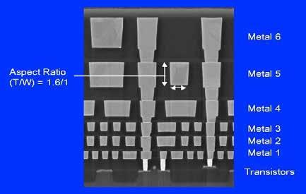
6 SEM MICRO-GRAPH (ILM DIELECTRIC REMOVED) METAL 2 W VIA W CONTACT METAL 1 METAL 1 POLYCIDE 10/18/18 Courtesy: IBM VLSI-1 Class Notes 6 5

7 Advanced Metallization Digital Integrated Circuits 2nd Page 7
, p. 5. 10/18/18 VLSI-1 Class Notes Page 8")
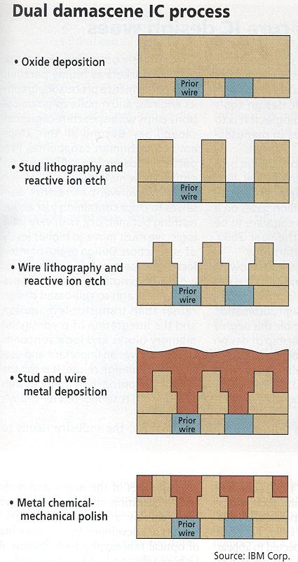
8 Interconnect Process Dual Damascene C.-K. Hu and J.M.E. Harper, Mater. Chem. Phys., 52 (1998), p /18/18 VLSI-1 Class Notes Page 8
9 WIRE GEOMETRY PITCH = width + space Height (h) = distance to top/bottom routes ASPECT RATIO (AR) = thickness / width Deep submicron processes have AR < 2 to maintain sheet resistances at a reasonable level Coupling to neighboring routes dominates w s Ll R=rL/tw t h Page 9 7
10 Wire Resistance r = resistivity (W*m) R r l = = R! t w l w where r=resistivity w w R o = sheet resistance (W/o) o is a dimensionless unit(!) Count number of squares R = R o * (# of squares) l w l l t t 1 Rectangular Block R = R (L/W) W 4 Rectangular Blocks R = R (2L/2W) W = R (L/W) W Page 10
11 Sheet Resistance Typical sheet resistances in 180 nm process Layer Sheet Resistance (W/o) Diffusion (silicided) 3-10 Diffusion (no silicide) Polysilicon (silicided) 3-10 Polysilicon (no silicide) Metal Metal Metal Metal Metal Metal Page 11
12 CONTRIBUTION OF WIRES (they are not free) DELAY Function of R, L and C, VIA resistance, local.vs. global POWER Charging/discharging of C is a function of CV2F NOISE Attackers/victims impact on functionality and delay POWER SUPPLY IR DROPS and GROUND BOUNCE Affects delay leading to timing failures RELIABILITY Electro-migration, self heat, maximum current COST Number of layers.vs. area/performance targets, yield Page 12

13 Contact/VIA Resistance Contacts and vias also have 2-20 W resistance Use many contacts for lower R Many small contacts for current crowding around periphery Page 13
14 Wire Capacitance Wire has capacitance per unit length To neighbors To layers above and below C total = C top + C bot + 2C adj s w layer n+1 h 2 C top t layer n h 1 C bot C adj layer n-1 Page 14
15 Capacitance Trends Parallel plate equation: C = ea/d Wires are not parallel plates, but obey trends Increasing area (W, t) increases capacitance Increasing distance (s, h) decreases capacitance Dielectric constant e = ke 0 e 0 = 8.85 x F/cm k = 3.9 for SiO 2 Processes are starting to use low-k dielectrics k» 3 (or less) as dielectrics use air pockets Page 15
16 M2 Capacitance Data Typical wires have ~ 0.2 ff/µm Compare to 2 ff/µm for gate capacitance C total (af/µm) M1, M3 planes s = 320 s = 480 s = 640 s= Isolated s = 320 s = 480 s = 640 s= w (nm) Page 16
17 Diffusion & Polysilicon Diffusion capacitance is very high (about 2 ff/µm) Comparable to gate capacitance Diffusion also has high resistance Avoid using diffusion runners for wires! Polysilicon has lower C but high R Use for transistor gates Occasionally for very short wires between gates Page 17
18 Lumped Element Models Wires are a distributed system Approximate with lumped element models N segments R R/N R/N R/N R/N C C/N C/N C/N C/N R R R/2 R/2 C C/2 C/2 C L-model p-model T-model 3-segment p-model is accurate to 3% in simulation L-model needs 100 segments for same accuracy! Use single segment p-model for Elmore delay Page 18
19 Example Metal2 wire in 180 nm process 5 mm long 0.32 µm wide Construct a 3-segment p-model R o = 0.05 W/o => R = 781 W C permicron = 0.2 ff/µm => C = 1 pf 260 W 167 ff 167 ff 260 W 167 ff 167 ff 260 W 167 ff 167 ff Page 19
20 Wire RC Delay Estimate the delay of a 10x inverter driving a 2x inverter at the end of the 5mm wire from the previous example. R = 2.5 kw*µm for gates Unit inverter: 0.36 µm nmos, 0.72 µm pmos t pd = 1.1 ns 781 W 690 W 500 ff 500 ff 4 ff Driver Wire Load Page 20
21 Crosstalk A capacitor does not like to change its voltage instantaneously. A wire has high capacitance to its neighbor. When the neighbor switches from 1-> 0 or 0->1, the wire tends to switch too. Called capacitive coupling or crosstalk. Crosstalk effects Noise on non-switching wires Increased delay on switching wires Page 21
22 Crosstalk Delay Assume layers above and below on average are quiet A B Second terminal of capacitor can be ignored Model as C gnd = C top + C bot C gnd C adj C gnd Effective C adj depends on behavior of neighbors Miller Coupling Factor (MCF) B DV C eff(a) MCF Constant V DD C gnd + C adj 1 Switching with A 0 C gnd 0 Switching opposite A 2V DD C gnd + 2 C adj 2 Page 22
23 Crosstalk Noise Crosstalk causes [functional/voltage] noise on nonswitching wires If victim is floating: model as capacitive voltage divider V C adj D victim = D Cgnd -v + Cadj Aggressor V aggressor DV aggressor Victim C adj C gnd-v DV victim Page 23
24 Driven Victims Usually victim is driven by a gate that fights noise Noise depends on relative resistances Victim driver is in linear region, aggressor in saturation If sizes are same, R aggressor = 2-4 x R victim Cadj 1 D Vvictim = DV C + C 1+ k gnd -v adj aggressor k t aggressor = = t ( ) - + ( ) - + R C C aggressor gnd a adj R C C victim victim gnd v adj R aggressor Aggressor DV aggressor C gnd-a C adj R victim Victim C gnd-v DV victim Page 24
25 Coupling Waveforms Simulated coupling for C adj = C victim 1.8 Aggressor Victim (undriven): 50% Victim (half size driver): 16% Victim (equal size driver): 8% Victim (double size driver): 4% t ( p s ) Page 25
26 Noise Implications Do we care if we have noise? If the noise is less than the noise margin, nothing happens Static CMOS logic will eventually settle to correct output even if disturbed by large noise spikes But glitches cause extra delay Also cause extra power from false transitions Dynamic logic never recovers from glitches Memories and other sensitive circuits also can produce the wrong answer 10/18/18 VLSI-1 Class Notes Page 26
27 Wire Engineering Goal: achieve delay, area, power goals with acceptable noise Degrees of freedom: Width Spacing Layer Shielding Delay (ns): RC/ Pitch (nm) Coupling: 2C adj / (2C adj +C gnd ) Pitch (nm) Wire Spacing (nm) vdd a 0 a 1 gnd a 2 a 3 vdd vdd a 0 gnd a 1 vdd a 2 gnd a 0 b 0 a 1 b 1 a 2 b 2 Page 27
28 Repeaters R and C are proportional to L RC delay is proportional to L 2 Unacceptably great for long wires Break long wires into N shorter segments Drive each one with an inverter or buffer Wire Length: l Driver Receiver l/n N Segments Segment l/n l/n Driver Repeater Repeater Repeater Receiver Page 28
29 Repeated Interconnect nm Copper Picoseconds M3 M4 M5 200 M Page 29
30 Repeater Design How many repeaters should we use? How large should each one be? Equivalent Circuit Wire length l Wire Capacitance C w *l & Resistance R w *l Inverter width W (nmos = W, pmos = 2W) Gate Capacitance C *W & Resistance R/W R w ln R/W C w l/2n C w l/2n C'W Page 30
31 Repeater Results Write equation for Elmore Delay Differentiate with respect to W and N Set equal to 0, solve ~60-80 ps/mm in 180 nm process Page 31
32 Repeater Placements Staggering the inverters Avoiding the Miller cap by opposite going signals Page 32
33 BACKUP Page 33
34 Layer Stack AMI 0.6 µm process has 3 metal layers Modern processes use metal layers Example: Intel 180 nm process M1: thin, narrow (< 3l) High density cells 1000 M2-M4: thicker For longer wires 1000 M5-M6: thickest For V DD, GND, clk 700 Layer T (nm) W (nm) S (nm) AR Substrate Page 34
Interconnect. Courtesy of Dr. Daehyun Dr. Dr. Shmuel and Dr.
 Interconnect Courtesy of Dr. Daehyun Lim@WSU, Dr. Harris@HMC, Dr. Shmuel Wimer@BIU and Dr. Choi@PSU http://csce.uark.edu +1 (479) 575-6043 yrpeng@uark.edu Introduction Chips are mostly made of wires called
Chapter 4. Problems. 1 Chapter 4 Problem Set
 1 Chapter 4 Problem Set Chapter 4 Problems 1. [M, None, 4.x] Figure 0.1 shows a clock-distribution network. Each segment of the clock network (between the nodes) is 5 mm long, 3 µm wide, and is implemented
Switching (AC) Characteristics of MOS Inverters. Prof. MacDonald
 Characteristics of MOS Inverters. Prof. MacDonald") Switching (AC) Characteristics of MOS Inverters Prof. MacDonald 1 MOS Inverters l Performance is inversely proportional to delay l Delay is time to raise (lower) voltage at nodes node voltage is changed
Switching (AC) Characteristics of MOS Inverters Prof. MacDonald 1 MOS Inverters l Performance is inversely proportional to delay l Delay is time to raise (lower) voltage at nodes node voltage is changed
EE141-Spring 2007 Digital Integrated Circuits
 EE141-Spring 2007 Digital Integrated Circuits Lecture 22 I/O, Power Distribution dders 1 nnouncements Homework 9 has been posted Due Tu. pr. 24, 5pm Project Phase 4 (Final) Report due Mo. pr. 30, noon
ECE 5745 Complex Digital ASIC Design Topic 2: CMOS Devices
 ECE 5745 Complex Digital ASIC Design Topic 2: CMOS Devices Christopher Batten School of Electrical and Computer Engineering Cornell University http://www.csl.cornell.edu/courses/ece5950 Simple Transistor
Introduction to CMOS VLSI Design (E158) Lecture 9: Cell Design
 Lecture 9: Cell Design") Harris Introduction to CMOS VLSI Design (E158) Lecture 9: Cell Design David Harris Harvey Mudd College David_Harris@hmc.edu Based on EE271 developed by Mark Horowitz, Stanford University MAH E158 Lecture
Harris Introduction to CMOS VLSI Design (E158) Lecture 9: Cell Design David Harris Harvey Mudd College David_Harris@hmc.edu Based on EE271 developed by Mark Horowitz, Stanford University MAH E158 Lecture
Lecture #2 Solving the Interconnect Problems in VLSI
 Lecture #2 Solving the Interconnect Problems in VLSI C.P. Ravikumar IIT Madras - C.P. Ravikumar 1 Interconnect Problems Interconnect delay has become more important than gate delays after 130nm technology
Interconnect/Via CONCORDIA VLSI DESIGN LAB
 Interconnect/Via 1 Delay of Devices and Interconnect 2 Reduction of the feature size Increase in the influence of the interconnect delay on system performance Skew The difference in the arrival times of
Lecture 9: Cell Design Issues
 Lecture 9: Cell Design Issues MAH, AEN EE271 Lecture 9 1 Overview Reading W&E 6.3 to 6.3.6 - FPGA, Gate Array, and Std Cell design W&E 5.3 - Cell design Introduction This lecture will look at some of the
2009 Spring CS211 Digital Systems & Lab 1 CHAPTER 3: TECHNOLOGY (PART 2)
") 1 CHAPTER 3: IMPLEMENTATION TECHNOLOGY (PART 2) Whatwillwelearninthischapter? we learn in this 2 How transistors operate and form simple switches CMOS logic gates IC technology FPGAs and other PLDs Basic
1 CHAPTER 3: IMPLEMENTATION TECHNOLOGY (PART 2) Whatwillwelearninthischapter? we learn in this 2 How transistors operate and form simple switches CMOS logic gates IC technology FPGAs and other PLDs Basic
EE 42/100 Lecture 23: CMOS Transistors and Logic Gates. Rev A 4/15/2012 (10:39 AM) Prof. Ali M. Niknejad
 Prof. Ali M. Niknejad") A. M. Niknejad University of California, Berkeley EE 100 / 42 Lecture 23 p. 1/16 EE 42/100 Lecture 23: CMOS Transistors and Logic Gates ELECTRONICS Rev A 4/15/2012 (10:39 AM) Prof. Ali M. Niknejad University
A. M. Niknejad University of California, Berkeley EE 100 / 42 Lecture 23 p. 1/16 EE 42/100 Lecture 23: CMOS Transistors and Logic Gates ELECTRONICS Rev A 4/15/2012 (10:39 AM) Prof. Ali M. Niknejad University
Closed-Form Expressions for Interconnection Delay, Coupling, and Crosstalk in VLSI s
 Closed-Form Expressions for Interconnection Delay, Coupling, and Crosstalk in VLSI s author Dr. Takayasu Sakurai Semiconductor Device Engnieering Laboratory, Toshiba Corporation, Tokoyo, Japan IEEE Transaction
Topic 3. CMOS Fabrication Process
 Topic 3 CMOS Fabrication Process Peter Cheung Department of Electrical & Electronic Engineering Imperial College London URL: www.ee.ic.ac.uk/pcheung/ E-mail: p.cheung@ic.ac.uk Lecture 3-1 Layout of a Inverter
ECE 484 VLSI Digital Circuits Fall Lecture 02: Design Metrics
 ECE 484 VLSI Digital Circuits Fall 2016 Lecture 02: Design Metrics Dr. George L. Engel Adapted from slides provided by Mary Jane Irwin (PSU) [Adapted from Rabaey s Digital Integrated Circuits, 2002, J.
Deep Submicron Interconnect. 0.18um vs. 013um Interconnect
 Deep Submicron Interconnect R. Dept. of ECE University of British Columbia res@ece.ubc.ca 0.18um vs. 013um Interconnect 0.18µm 5-layer Al Metal Process 0.13µm 8-layer Cu Metal Process 1 Interconnect Scaling
ECE520 VLSI Design. Lecture 2: Basic MOS Physics. Payman Zarkesh-Ha
 ECE520 VLSI Design Lecture 2: Basic MOS Physics Payman Zarkesh-Ha Office: ECE Bldg. 230B Office hours: Wednesday 2:00-3:00PM or by appointment E-mail: pzarkesh@unm.edu Slide: 1 Review of Last Lecture Semiconductor
Microcircuit Electrical Issues
 Microcircuit Electrical Issues Distortion The frequency at which transmitted power has dropped to 50 percent of the injected power is called the "3 db" point and is used to define the bandwidth of the
High-speed Serial Interface
 High-speed Serial Interface Lect. 9 Noises 1 Block diagram Where are we today? Serializer Tx Driver Channel Rx Equalizer Sampler Deserializer PLL Clock Recovery Tx Rx 2 Sampling in Rx Interface applications
Digital Integrated Circuits Designing Combinational Logic Circuits. Fuyuzhuo
 Digital Integrated Circuits Designing Combinational Logic Circuits Fuyuzhuo Introduction Digital IC Combinational vs. Sequential Logic In Combinational Logic Circuit Out In Combinational Logic Circuit
Modeling the Effect of Wire Resistance in Deep Submicron Coupled Interconnects for Accurate Crosstalk Based Net Sorting
 Modeling the Effect of Wire Resistance in Deep Submicron Coupled Interconnects for Accurate Crosstalk Based Net Sorting C. Guardiani, C. Forzan, B. Franzini, D. Pandini Adanced Research, Central R&D, DAIS,
Signal Integrity Design of TSV-Based 3D IC
 Signal Integrity Design of TSV-Based 3D IC October 24, 21 Joungho Kim at KAIST joungho@ee.kaist.ac.kr http://tera.kaist.ac.kr 1 Contents 1) Driving Forces of TSV based 3D IC 2) Signal Integrity Issues
5. CMOS Gates: DC and Transient Behavior
 5. CMOS Gates: DC and Transient Behavior Jacob Abraham Department of Electrical and Computer Engineering The University of Texas at Austin VLSI Design Fall 2017 September 18, 2017 ECE Department, University
PHYSICAL STRUCTURE OF CMOS INTEGRATED CIRCUITS. Dr. Mohammed M. Farag
 PHYSICAL STRUCTURE OF CMOS INTEGRATED CIRCUITS Dr. Mohammed M. Farag Outline Integrated Circuit Layers MOSFETs CMOS Layers Designing FET Arrays EE 432 VLSI Modeling and Design 2 Integrated Circuit Layers
Layout of a Inverter. Topic 3. CMOS Fabrication Process. The CMOS Process - photolithography (2) The CMOS Process - photolithography (1) v o.
 The CMOS Process - photolithography (1) v o.") Layout of a Inverter Topic 3 CMOS Fabrication Process V DD Q p Peter Cheung Department of Electrical & Electronic Engineering Imperial College London v i v o Q n URL: www.ee.ic.ac.uk/pcheung/ E-mail: p.cheung@ic.ac.uk
Layout of a Inverter Topic 3 CMOS Fabrication Process V DD Q p Peter Cheung Department of Electrical & Electronic Engineering Imperial College London v i v o Q n URL: www.ee.ic.ac.uk/pcheung/ E-mail: p.cheung@ic.ac.uk
19. Design for Low Power
 19. Design for Low Power Jacob Abraham Department of Electrical and Computer Engineering The University of Texas at Austin VLSI Design Fall 2017 November 8, 2017 ECE Department, University of Texas at
Digital Integrated Circuits Designing Combinational Logic Circuits. Fuyuzhuo
 Digital Integrated Circuits Designing Combinational Logic Circuits Fuyuzhuo Introduction Digital IC Combinational vs. Sequential Logic In Combinational Logic Circuit Out In Combinational Logic Circuit
EE434 ASIC & Digital Systems. Partha Pande School of EECS Washington State University
 EE434 ASIC & Digital Systems Partha Pande School of EECS Washington State University pande@eecs.wsu.edu Lecture 11 Physical Design Issues Interconnect Scaling Effects Dense multilayer metal increases coupling
ELEC Digital Logic Circuits Fall 2015 Delay and Power
 ELEC - Digital Logic Circuits Fall 5 Delay and Power Vishwani D. Agrawal James J. Danaher Professor Department of Electrical and Computer Engineering Auburn University, Auburn, AL 36849 http://www.eng.auburn.edu/~vagrawal
Jack Keil Wolf Lecture. ESE 570: Digital Integrated Circuits and VLSI Fundamentals. Lecture Outline. MOSFET N-Type, P-Type.
 ESE 570: Digital Integrated Circuits and VLSI Fundamentals Jack Keil Wolf Lecture Lec 3: January 24, 2019 MOS Fabrication pt. 2: Design Rules and Layout http://www.ese.upenn.edu/about-ese/events/wolf.php
04/29/03 EE371 Power Delivery D. Ayers 1. VLSI Power Delivery. David Ayers
 04/29/03 EE371 Power Delivery D. Ayers 1 VLSI Power Delivery David Ayers 04/29/03 EE371 Power Delivery D. Ayers 2 Outline Die power delivery Die power goals Typical processor power grid Transistor power
5/1/2011. o We will focus on challenges facing Interconnect scaling and. will seek solutions and new opportunities
 Session 1: Trends in VLSI 1 o We will focus on challenges facing Interconnect scaling and will seek solutions and new opportunities o There will be no design project, while some simulations will be needed
UNIT III VLSI CIRCUIT DESIGN PROCESSES. In this chapter we will be studying how to get the schematic into stick diagrams or layouts.
 UNIT III VLSI CIRCUIT DESIGN PROCESSES In this chapter we will be studying how to get the schematic into stick diagrams or layouts. MOS circuits are formed on four basic layers: N-diffusion P-diffusion
Module-3: Metal Oxide Semiconductor (MOS) & Emitter coupled logic (ECL) families
 & Emitter coupled logic (ECL) families") 1 Module-3: Metal Oxide Semiconductor (MOS) & Emitter coupled logic (ECL) families 1. Introduction 2. Metal Oxide Semiconductor (MOS) logic 2.1. Enhancement and depletion mode 2.2. NMOS and PMOS inverter
1 Module-3: Metal Oxide Semiconductor (MOS) & Emitter coupled logic (ECL) families 1. Introduction 2. Metal Oxide Semiconductor (MOS) logic 2.1. Enhancement and depletion mode 2.2. NMOS and PMOS inverter
Microcontroller Systems. ELET 3232 Topic 13: Load Analysis
 Microcontroller Systems ELET 3232 Topic 13: Load Analysis 1 Objective To understand hardware constraints on embedded systems Define: Noise Margins Load Currents and Fanout Capacitive Loads Transmission
problem grade total
 Fall 2005 6.012 Microelectronic Devices and Circuits Prof. J. A. del Alamo Name: Recitation: November 16, 2005 Quiz #2 problem grade 1 2 3 4 total General guidelines (please read carefully before starting):
ESE 570: Digital Integrated Circuits and VLSI Fundamentals
 ESE 570: Digital Integrated Circuits and VLSI Fundamentals Lec 3: January 24, 2019 MOS Fabrication pt. 2: Design Rules and Layout Penn ESE 570 Spring 2019 Khanna Jack Keil Wolf Lecture http://www.ese.upenn.edu/about-ese/events/wolf.php
MOSFETS: Gain & non-linearity
 MOFET: ain & non-linearity source gate Polysilicon wire Heavily doped (n-type or p-type) diffusions W Inter-layer io 2 insulation Very thin (
Basic Fabrication Steps
 Basic Fabrication Steps and Layout Somayyeh Koohi Department of Computer Engineering Adapted with modifications from lecture notes prepared by author Outline Fabrication steps Transistor structures Transistor
Homework 10 posted just for practice. Office hours next week, schedule TBD. HKN review today. Your feedback is important!
 EE141 Fall 2005 Lecture 26 Memory (Cont.) Perspectives Administrative Stuff Homework 10 posted just for practice No need to turn in Office hours next week, schedule TBD. HKN review today. Your feedback
EE4800 CMOS Digital IC Design & Analysis. Lecture 1 Introduction Zhuo Feng
 EE4800 CMOS Digital IC Design & Analysis Lecture 1 Introduction Zhuo Feng 1.1 Prof. Zhuo Feng Office: EERC 730 Phone: 487-3116 Email: zhuofeng@mtu.edu Class Website http://www.ece.mtu.edu/~zhuofeng/ee4800fall2010.html
Introduction. Digital Integrated Circuits A Design Perspective. Jan M. Rabaey Anantha Chandrakasan Borivoje Nikolic. July 30, 2002
 Digital Integrated Circuits A Design Perspective Jan M. Rabaey Anantha Chandrakasan Borivoje Nikolic Introduction July 30, 2002 1 What is this book all about? Introduction to digital integrated circuits.
EE115C Winter 2017 Digital Electronic Circuits. Lecture 11: Wires, Elmore Delay
 EE115C Winter 2017 Digital Electronic Circuits Lecture 11: Wires, Elmore Delay The Wire transmitters receivers schematics physical EE115C Winter 2017 2 Interconnect Impact on Chip EE115C Winter 2017 3
Lecture 04 CSE 40547/60547 Computing at the Nanoscale Interconnect
 Lecture 04 CSE 40547/60547 Computing at the Nanoscale Interconnect Introduction - So far, have considered transistor-based logic in the face of technology scaling - Interconnect effects are also of concern
Integrated diodes. The forward voltage drop only slightly depends on the forward current. ELEKTRONIKOS ĮTAISAI
 1 Integrated diodes pn junctions of transistor structures can be used as integrated diodes. The choice of the junction is limited by the considerations of switching speed and breakdown voltage. The forward
Lecture 12 Memory Circuits. Memory Architecture: Decoders. Semiconductor Memory Classification. Array-Structured Memory Architecture RWM NVRWM ROM
 Semiconductor Memory Classification Lecture 12 Memory Circuits RWM NVRWM ROM Peter Cheung Department of Electrical & Electronic Engineering Imperial College London Reading: Weste Ch 8.3.1-8.3.2, Rabaey
Lecture 07 Modeling and Optimization of VLSI Interconnects (ECG 415/615 Introduction to VLSI System Design)
") Lecture 07 Modeling and Optimization of VLSI Interconnects (ECG 415/615 Introduction to VLSI System Design) Dr. Yingtao Jiang Department of Electrical and Computer Engineering University of Nevada Las
Lecture 07 Modeling and Optimization of VLSI Interconnects (ECG 415/615 Introduction to VLSI System Design) Dr. Yingtao Jiang Department of Electrical and Computer Engineering University of Nevada Las
420 Intro to VLSI Design
 Dept of Electrical and Computer Engineering 420 Intro to VLSI Design Lecture 0: Course Introduction and Overview Valencia M. Joyner Spring 2005 Getting Started Syllabus About the Instructor Labs, Problem
Trends and Challenges in VLSI Technology Scaling Towards 100nm
 Trends and Challenges in VLSI Technology Scaling Towards 100nm Stefan Rusu Intel Corporation stefan.rusu@intel.com September 2001 Stefan Rusu 9/2001 2001 Intel Corp. Page 1 Agenda VLSI Technology Trends
Introduction to VLSI ASIC Design and Technology
 Introduction to VLSI ASIC Design and Technology Paulo Moreira CERN - Geneva, Switzerland Paulo Moreira Introduction 1 Outline Introduction Is there a limit? Transistors CMOS building blocks Parasitics
Lecture Notes 5 CMOS Image Sensor Device and Fabrication
 Lecture Notes 5 CMOS Image Sensor Device and Fabrication CMOS image sensor fabrication technologies Pixel design and layout Imaging performance enhancement techniques Technology scaling, industry trends
ECE 497 JS Lecture - 22 Timing & Signaling
 ECE 497 JS Lecture - 22 Timing & Signaling Spring 2004 Jose E. Schutt-Aine Electrical & Computer Engineering University of Illinois jose@emlab.uiuc.edu 1 Announcements - Signaling Techniques (4/27) - Signaling
Static Random Access Memory - SRAM Dr. Lynn Fuller Webpage:
 ROCHESTER INSTITUTE OF TECHNOLOGY MICROELECTRONIC ENGINEERING Static Random Access Memory - SRAM Dr. Lynn Fuller Webpage: http://people.rit.edu/lffeee 82 Lomb Memorial Drive Rochester, NY 14623-5604 Email:
Power Spring /7/05 L11 Power 1
 Power 6.884 Spring 2005 3/7/05 L11 Power 1 Lab 2 Results Pareto-Optimal Points 6.884 Spring 2005 3/7/05 L11 Power 2 Standard Projects Two basic design projects Processor variants (based on lab1&2 testrigs)
EE 330 Lecture 43. Digital Circuits. Other Logic Styles Dynamic Logic Circuits
 EE 330 Lecture 43 Digital Circuits Other Logic Styles Dynamic Logic Circuits Review from Last Time Elmore Delay Calculations W M 5 V OUT x 20C RE V IN 0 L R L 1 L R RW 6 W 1 C C 3 D R t 1 R R t 2 R R t
Lecture 020 ECE4430 Review II (1/5/04) Page 020-1
 Page 020-1") Lecture 020 ECE4430 Review II (1/5/04) Page 020-1 LECTURE 020 ECE 4430 REVIEW II (READING: GHLM - Chap. 2) Objective The objective of this presentation is: 1.) Identify the prerequisite material as taught
Lecture 020 ECE4430 Review II (1/5/04) Page 020-1 LECTURE 020 ECE 4430 REVIEW II (READING: GHLM - Chap. 2) Objective The objective of this presentation is: 1.) Identify the prerequisite material as taught
Transistor was first invented by William.B.Shockley, Walter Brattain and John Bardeen of Bell Labratories. In 1961, first IC was introduced.
 Unit 1 Basic MOS Technology Transistor was first invented by William.B.Shockley, Walter Brattain and John Bardeen of Bell Labratories. In 1961, first IC was introduced. Levels of Integration:- i) SSI:-
Signal Integrity for Gigascale SOC Design. Professor Lei He ECE Department University of Wisconsin, Madison
 Signal Integrity for Gigascale SOC Design Professor Lei He ECE Department University of Wisconsin, Madison he@ece.wisc.edu http://eda.ece.wisc.edu Outline Capacitive noise Technology trends Capacitance
EE141- Spring 2004 Digital Integrated Circuits
 EE141- Spring 2004 Digital Integrated Circuits Lecture 27 Power distribution Resistive interconnect 1 Administrative Stuff Make-up lecture on Monday 4-5:30pm Special office hours of Prof. Rabaey today
Layout - Line of Diffusion. Where are we? Line of Diffusion in General. Line of Diffusion in General. Stick Diagrams. Line of Diffusion in General
 Where are we? Lots of Layout issues Line of diffusion style Power pitch it-slice pitch Routing strategies Transistor sizing Wire sizing Layout - Line of Diffusion Very common layout method Start with a
UNIT-1 Bipolar Junction Transistors. Text Book:, Microelectronic Circuits 6 ed., by Sedra and Smith, Oxford Press
 UNIT-1 Bipolar Junction Transistors Text Book:, Microelectronic Circuits 6 ed., by Sedra and Smith, Oxford Press Figure 6.1 A simplified structure of the npn transistor. Microelectronic Circuits, Sixth
EE 330 Lecture 43. Digital Circuits. Other Logic Styles Dynamic Logic Circuits
 EE 330 Lecture 43 Digital Circuits Other Logic Styles Dynamic Logic Circuits Review from Last Time Elmore Delay Calculations W M 5 V OUT x 20C RE V IN 0 L R L 1 L R R 6 W 1 C C 3 D R t 1 R R t 2 R R t
VLSI Design I; A. Milenkovic 1
 CPE/EE 427, CPE 527 VLSI Design I L02: Design Metrics Department of Electrical and Computer Engineering University of Alabama in Huntsville Aleksandar Milenkovic ( www.ece.uah.edu/~milenka ) www.ece.uah.edu/~milenka/cpe527-03f
Lecture 16. Complementary metal oxide semiconductor (CMOS) CMOS 1-1
 CMOS 1-1") Lecture 16 Complementary metal oxide semiconductor (CMOS) CMOS 1-1 Outline Complementary metal oxide semiconductor (CMOS) Inverting circuit Properties Operating points Propagation delay Power dissipation
Lecture 16 Complementary metal oxide semiconductor (CMOS) CMOS 1-1 Outline Complementary metal oxide semiconductor (CMOS) Inverting circuit Properties Operating points Propagation delay Power dissipation
Microelectronics, BSc course
 Microelectronics, BSc course MOS circuits: CMOS circuits, construction http://www.eet.bme.hu/~poppe/miel/en/14-cmos.pptx http://www.eet.bme.hu The abstraction level of our study: SYSTEM + MODULE GATE CIRCUIT
Advanced Digital Design
 Advanced Digital Design Introduction & Motivation by A. Steininger and M. Delvai Vienna University of Technology Outline Challenges in Digital Design The Role of Time in the Design The Fundamental Design
Panasonic DMC-GH Mp, 4.4 µm Pixel Size LiveMOS Image Sensor from Panasonic LUMIX DMC-GH1 Micro Four Thirds Digital Interchangeable Lens Camera
 Panasonic DMC-GH1 12.1 Mp, 4.4 µm Pixel Size LiveMOS Image Sensor from Panasonic LUMIX DMC-GH1 Micro Four Thirds Digital Interchangeable Lens Camera Imager Process Review For comments, questions, or more
1 Digital EE141 Integrated Circuits 2nd Introduction
 Digital Integrated Circuits Introduction 1 What is this lecture about? Introduction to digital integrated circuits + low power circuits Issues in digital design The CMOS inverter Combinational logic structures
+1 (479)
") Introduction to VLSI Design http://csce.uark.edu +1 (479) 575-6043 yrpeng@uark.edu Invention of the Transistor Vacuum tubes ruled in first half of 20th century Large, expensive, power-hungry, unreliable
Introduction to VLSI Design http://csce.uark.edu +1 (479) 575-6043 yrpeng@uark.edu Invention of the Transistor Vacuum tubes ruled in first half of 20th century Large, expensive, power-hungry, unreliable
Preface to Third Edition Deep Submicron Digital IC Design p. 1 Introduction p. 1 Brief History of IC Industry p. 3 Review of Digital Logic Gate
 Preface to Third Edition p. xiii Deep Submicron Digital IC Design p. 1 Introduction p. 1 Brief History of IC Industry p. 3 Review of Digital Logic Gate Design p. 6 Basic Logic Functions p. 6 Implementation
EEC 118 Lecture #12: Dynamic Logic
 EEC 118 Lecture #12: Dynamic Logic Rajeevan Amirtharajah University of California, Davis Jeff Parkhurst Intel Corporation Outline Today: Alternative MOS Logic Styles Dynamic MOS Logic Circuits: Rabaey
Lecture 10. Circuit Pitfalls
 Lecture 10 Circuit Pitfalls Intel Corporation jstinson@stanford.edu 1 Overview Reading Lev Signal and Power Network Integrity Chandrakasen Chapter 7 (Logic Families) and Chapter 8 (Dynamic logic) Gronowski
Lecture 13 CMOS Power Dissipation
 EE 471: Transport Phenomena in Solid State Devices Spring 2018 Lecture 13 CMOS Power Dissipation Bryan Ackland Department of Electrical and Computer Engineering Stevens Institute of Technology Hoboken,
EECS 141: SPRING 98 FINAL
 University of California College of Engineering Department of Electrical Engineering and Computer Science J. M. Rabaey 511 Cory Hall TuTh3:3-5pm e141@eecs EECS 141: SPRING 98 FINAL For all problems, you
ESE370: Circuit-Level Modeling, Design, and Optimization for Digital Systems. Today. Variation. Variation. Process Corners.
 ESE370: Circuit-Level Modeling, Design, and Optimization for Digital Systems Day 13: October 3, 2012 Layout and Area Today Coping with Variation (from last time) Layout Transistors Gates Design rules Standard
VLSI: An Introduction
 Chapter 1 UEEA2223/UEEG4223 Integrated Circuit Design VLSI: An Introduction Prepared by Dr. Lim Soo King 02 Jan 2011. Chapter 1 VLSI Design: An Introduction... 1 1.0 Introduction... 1 1.0.1 Early Computing
! Review: MOS IV Curves and Switch Model. ! MOS Device Layout. ! Inverter Layout. ! Gate Layout and Stick Diagrams. ! Design Rules. !
 ESE 570: Digital Integrated Circuits and VLSI Fundamentals Lec 3: January 21, 2017 MOS Fabrication pt. 2: Design Rules and Layout Lecture Outline! Review: MOS IV Curves and Switch Model! MOS Device Layout!
Review and Analysis of Glitch Reduction for Low Power VLSI Circuits
 Review and Analysis of Glitch Reduction for Low Power VLSI Circuits Somashekhar Malipatil 1 1 Assistant Professor Department of Electronics & Communication Engineering Nalla Malla Reddy Engineering College,
LSI Logic LSI53C1030 PCI-X to Dual Channel Ultra320 SCSI Controller 0.18 µm CMOS Process
 LSI Logic LSI53C13 PCI-X to Dual Channel Ultra32 SCSI Controller.18 µm CMOS Process Structural Analysis For comments, questions, or more information about this report, or for any additional technical needs
Written Examination on. Wednesday October 17, 2007,
 Written Examination on Wednesday October 17, 2007, 08.00-12.00 The textbook and a calculator are allowed on the examination 1. The following logical function is given Q= AB( CD+ CE) + F a. Draw the schematic
d. Can you find intrinsic gain more easily by examining the equation for current? Explain.
 EECS140 Final Spring 2017 Name SID 1. [8] In a vacuum tube, the plate (or anode) current is a function of the plate voltage (output) and the grid voltage (input). I P = k(v P + µv G ) 3/2 where µ is a
Interconnect-Power Dissipation in a Microprocessor
 4/2/2004 Interconnect-Power Dissipation in a Microprocessor N. Magen, A. Kolodny, U. Weiser, N. Shamir Intel corporation Technion - Israel Institute of Technology 4/2/2004 2 Interconnect-Power Definition
Integrated Circuits & Systems
 Federal University of Santa atarina enter for Technology omputer Science & Electronics Engineering Integrated ircuits & Systems INE 5442 Lecture 16 MOS ombinational ircuits - 2 guntzel@inf.ufsc.br Pass
! MOS Device Layout. ! Inverter Layout. ! Gate Layout and Stick Diagrams. ! Design Rules. ! Standard Cells. ! CMOS Process Enhancements
 EE 570: igital Integrated Circuits and VLI Fundamentals Lec 3: January 18, 2018 MO Fabrication pt. 2: esign Rules and Layout Lecture Outline! MO evice Layout! Inverter Layout! Gate Layout and tick iagrams!
Chapter 15 Summary and Future Trends
 Chapter 15 Summary and Future Trends Hong Xiao, Ph. D. hxiao89@hotmail.com www2.austin.cc.tx.us/hongxiao/book.htm Hong Xiao, Ph. D. www2.austin.cc.tx.us/hongxiao/book.htm 1 The 1960s First IC product Bipolar
Deep Trench Capacitors for Switched Capacitor Voltage Converters
 Deep Trench Capacitors for Switched Capacitor Voltage Converters Jae-sun Seo, Albert Young, Robert Montoye, Leland Chang IBM T. J. Watson Research Center 3 rd International Workshop for Power Supply on
Panasonic DMC-GH Mp, 4.4 µm Pixel Size LiveMOS Image Sensor from Panasonic LUMIX DMC-GH1 Micro Four Thirds Digital Interchangeable Lens Camera
 Panasonic DMC-GH1 12.1 Mp, 4.4 µm Pixel Size LiveMOS Image Sensor from Panasonic LUMIX DMC-GH1 Micro Four Thirds Digital Interchangeable Lens Camera Imager Process Review For comments, questions, or more
Powerchip Semiconductor Corporation A3R12E3GEF G6E 635BLC4M 512 Megabit DDR2 SDRAM Structural Analysis
 February 23, 2007 Powerchip Semiconductor Corporation A3R12E3GEF G6E 635BLC4M Structural Analysis For comments, questions, or more information about this report, or for any additional technical needs concerning
Lecture 0: Introduction
 Lecture 0: Introduction Introduction Integrated circuits: many transistors on one chip. Very Large Scale Integration (VLSI): bucketloads! Complementary Metal Oxide Semiconductor Fast, cheap, low power
Digital Integrated Circuits Lecture 20: Package, Power, Clock, and I/O
 Digital Integrated Circuits Lecture 20: Package, Power, Clock, and I/O Chih-Wei Liu VLSI Signal Processing LAB National Chiao Tung University cwliu@twins.ee.nctu.edu.tw DIC-Lec20 cwliu@twins.ee.nctu.edu.tw
Design of Low Power Vlsi Circuits Using Cascode Logic Style
 Design of Low Power Vlsi Circuits Using Cascode Logic Style Revathi Loganathan 1, Deepika.P 2, Department of EST, 1 -Velalar College of Enginering & Technology, 2- Nandha Engineering College,Erode,Tamilnadu,India
Conduction Characteristics of MOS Transistors (for fixed Vds)! Topic 2. Basic MOS theory & SPICE simulation. MOS Transistor
! Topic 2. Basic MOS theory & SPICE simulation. MOS Transistor") Conduction Characteristics of MOS Transistors (for fixed Vds)! Topic 2 Basic MOS theory & SPICE simulation Peter Cheung Department of Electrical & Electronic Engineering Imperial College London (Weste&Harris,
Conduction Characteristics of MOS Transistors (for fixed Vds)! Topic 2 Basic MOS theory & SPICE simulation Peter Cheung Department of Electrical & Electronic Engineering Imperial College London (Weste&Harris,
Topic 2. Basic MOS theory & SPICE simulation
 Topic 2 Basic MOS theory & SPICE simulation Peter Cheung Department of Electrical & Electronic Engineering Imperial College London (Weste&Harris, Ch 2 & 5.1-5.3 Rabaey, Ch 3) URL: www.ee.ic.ac.uk/pcheung/
Conduction Characteristics of MOS Transistors (for fixed Vds) Topic 2. Basic MOS theory & SPICE simulation. MOS Transistor
 Topic 2. Basic MOS theory & SPICE simulation. MOS Transistor") Conduction Characteristics of MOS Transistors (for fixed Vds) Topic 2 Basic MOS theory & SPICE simulation Peter Cheung Department of Electrical & Electronic Engineering Imperial College London (Weste&Harris,
Conduction Characteristics of MOS Transistors (for fixed Vds) Topic 2 Basic MOS theory & SPICE simulation Peter Cheung Department of Electrical & Electronic Engineering Imperial College London (Weste&Harris,
Digital Microelectronic Circuits ( ) Pass Transistor Logic. Lecture 9: Presented by: Adam Teman
 Pass Transistor Logic. Lecture 9: Presented by: Adam Teman") Digital Microelectronic Circuits (361-1-3021 ) Presented by: Adam Teman Lecture 9: Pass Transistor Logic 1 Motivation In the previous lectures, we learned about Standard CMOS Digital Logic design. CMOS
Digital Microelectronic Circuits (361-1-3021 ) Presented by: Adam Teman Lecture 9: Pass Transistor Logic 1 Motivation In the previous lectures, we learned about Standard CMOS Digital Logic design. CMOS
MOSFET & IC Basics - GATE Problems (Part - I)
") MOSFET & IC Basics - GATE Problems (Part - I) 1. Channel current is reduced on application of a more positive voltage to the GATE of the depletion mode n channel MOSFET. (True/False) [GATE 1994: 1 Mark]
MOSFET & IC Basics - GATE Problems (Part - I) 1. Channel current is reduced on application of a more positive voltage to the GATE of the depletion mode n channel MOSFET. (True/False) [GATE 1994: 1 Mark]
Lecture #29. Moore s Law
 Lecture #29 ANNOUNCEMENTS HW#15 will be for extra credit Quiz #6 (Thursday 5/8) will include MOSFET C-V No late Projects will be accepted after Thursday 5/8 The last Coffee Hour will be held this Thursday
ECE 334: Electronic Circuits Lecture 10: Digital CMOS Circuits
 Faculty of Engineering ECE 334: Electronic Circuits Lecture 10: Digital CMOS Circuits CMOS Technology Complementary MOS, or CMOS, needs both PMOS and NMOS FET devices for their logic gates to be realized
Design Simulation and Analysis of NMOS Characteristics for Varying Oxide Thickness
 MIT International Journal of Electronics and Communication Engineering, Vol. 4, No. 2, August 2014, pp. 81 85 81 Design Simulation and Analysis of NMOS Characteristics for Varying Oxide Thickness Alpana
Matrix Semiconductor One Time Programmable Memory
 December 22, 2004 Matrix Semiconductor 11247-01-99 One Time Programmable Memory Structural Analysis For questions, comments, or more information about this report, or for any additional technical needs