ELECTRONIC DEVICES AND CIRCUITS. Prepared By: Mr. N Ravi Teja Assistant Professor
|
|
|
- Joy Pope
- 6 years ago
- Views:
Transcription
1 ELECTRONIC DEVICES AND CIRCUITS Prepared By: Mr. N Ravi Teja Assistant Professor
2 Information Technology
3 Unit-1 PN Junction Diode & Special Function Electronic Devices
4 An atom is composed of : Atomic Structure Nucleus ( which contains positively charged protons and neutral neutrons) Electrons (which are négative charged and that orbit the nucleus)
5 Valence Electrons Electrons are distributed in various shells at different distances from nucleus Electron energy increases as shell radius increases. Electrons in the outer most Shell are called as valence electrons Elements in the period table are grouped according to the number of valence electrons.
6 Valence Electrons
7 Elemental/Compound Semiconductor Silicon (Si) and Germanium (Ge) are in group IV, and are elemental semiconductors Galium arsenide (GaAs) is a goup III-V compound semiconductor
8 Silicon Crystal At 0 K, each electron is in its lowest possible energy state, and each covalent bounding position is filled. If a small electric field is applied, the electrons will not move silicon is an insulator
9 Silicon Atom Diagram at 0 K
10 Intrinsic Silicon If the temperature increases, the valence electrons will gain some thermal energy, and breaks free from the covalent bond It leaves a positively charged hole In order to break from the covalent bond, a valence electron must gain a minimun energy Eg: Bandgap energy
11 Silicon Atom Diagram at Ambiant Temp
12 Insulators/Conductors Materials that have large bandgap energies (in the range of 3 to 6 electron-volts (ev)) are insulators, because at room temperature, essentially no free electron exists in the material Materials that contain very large number of free electrons at room temperature are conductors
13 Semiconductors In a semiconductor, the bandgap energy is in the order of 1 ev. The net flow of free electrons causes a current. In a semiconductor, two types of charged particles contribute to the current: the negatively charged electrons and the positively charged holes
14 Movement of Holes Movement of Holes
15 Semiconductor Constants The concentration of electrons and holes directly influence the magnitde of the current In an intrinsic semiconductor (a single crystal semiconductor) the densities of holes and electrons are equal.
16 ni: intrinsic carrier concentration for free electrons (same for holes) B: constant related to specific semiconductor material Eg: Bandgap energy (ev) T: Temperature ( K) K: Boltzman Constant (86 E-06 ev/ K)
17 Semiconductor Constants
18 Extrinsic Semiconductor / Doping The electron or hole concentration can be greatly increased by adding controlled amounts of certain impurities For silicon, it is desirable to use impurities from the group III and V. An N-type semiconductor can be created by adding phosphorus or arsenic
19 Extrinsic Semiconductor / Doping The phosphorus (group V) atom is called donor impurity because it donates an electron that is free to move The boron (group III) has accepted a valence electron (or donated a hole), it is therefore called acceptor impurity
20 N-Type Semiconductor
21 P-Type Semiconductor
22 Introduction to Semiconductor Devices Semiconductor p-n junction diodes
23 p-n junction formation p-type material Semiconductor material doped with acceptors. Material has high hole concentration Concentration of free electrons in p-type material is very low. n-type material Semiconductor material doped with donors. Material has high concentration of free electrons. Concentration of holes in n-type material is very low.
 and NEGATIVELY charged free electrons.")
24 p-n junction formation p-type material Contains NEGATIVELY charged acceptors (immovable) and POSITIVELY charged holes (free). Total charge = 0 n-type material Contains POSITIVELY charged donors (immovable) and NEGATIVELY charged free electrons. Total charge = 0

25 Diffusion A substance, the purple dots, in solution. A membrane prevents movement of the water and the molecules from crossing from one side of the beaker to the other. Now that the gates have been opened, the random movements of the molecules have caused, overtime, the number of molecules to be equal on the two sides of the barrier.
26 Diffusion As a result of diffusion, the molecules or other free particles distribute uniformly over the entire volume

27 p- n junction formation What happens if n- and p-type materials are in close contact? Being free particles, electrons start diffusing from n-type material into p-material Being free particles, holes, too, start diffusing from p-type material into n-material Have they been NEUTRAL particles, eventually all the free electrons and holes had uniformly distributed over the entire compound crystal. However, every electrons transfers a negative charge (-q) onto the p- side and also leaves an uncompensated (+q) charge of the donor on the n-side. Every hole creates one positive charge (q) on the n-side and (-q) on the p-side
28 p- n junction formation What happens if n- and p-type materials are in close contact? p-type n-type Electrons and holes remain staying close to the p-n junction because negative and positive charges attract each other. Negative charge stops electrons from further diffusion Positive charge stops holes from further diffusion The diffusion forms a dipole charge layer at the p-n junction interface. There is a built-in VOLTAGE at the p-n junction interface that prevents penetration of electrons into the p-side and holes into the n-side.
29 p- n junction current voltage characteristics What happens when the voltage is applied to a p-n junction? p-type n-type The polarity shown, attracts holes to the left and electrons to the right. According to the current continuity law, the current can only flow if all the charged particles move forming a closed loop However, there are very few holes in n-type material and there are very few electrons in the p-type material. There are very few carriers available to support the current through the junction plane For the voltage polarity shown, the current is nearly zero
30 p- n junction current voltage characteristics What happens if voltage of opposite polarity is applied to a p-n junction? p-type n-type The polarity shown, attracts electrons to the left and holes to the right. There are plenty of electrons in the n-type material and plenty of holes in the p-type material. There are a lot of carriers available to cross the junction. When the voltage applied is lower than the built-in voltage, the current is still nearly zero When the voltage exceeds the built-in voltage, the current can flow through the p-n junction
31 Diode current voltage (I-V) characteristics Semiconductor diode consists of a p-n junction with two contacts attached to the p- and n- sides V p n 0 qv I I exp 1 S kt I is usually a very small current, I A S S When the voltage V is negative ( reverse polarity) the exponential term - 1; The diode current is I S ( very small). When the voltage V is positive ( forward polarity) the exponential term increases rapidly with V and the current is high.

32 Graphing the I-V characteristics of electronic components. The I-V plot represents is the dependence of the current I through the component on the voltage V across it. Resistor 1 V I R; I V R I I = V / R; R = V/I R I tg( ) = 1/R V The I-V characteristic of the resistor V
33 The I-V characteristic of the diode qv I I exp 1 S kt I S
34 The experimental I-V characteristic of a Si
35 p- n diode circuit notation When plus is applied to the p-side, I I S the current is high. This voltage polarity is called FORWARD. I S When plus is applied to the n-side, the current is nearly zero. This voltage polarity is called REVERSE.

36 p- n diode applications: Light emitters + - P-n junction can emit the light when forward biased p-type n-type Electrons drift into p-material and find plenty of holes there. They RECOMBINE by filling up the empty positions. Holes drift into n-material and find plenty of electrons there. They also RECOMBINE by filling up the empty positions. The energy released in the process of annihilation produces PHOTONS the particles of light

37 - + When the light illuminates the p-n junction, the photons energy RELEASES free electrons and holes. They are referred to as PHOTO-ELECTRONS and PHOTO-HOLES The applied voltage separates the photo-carriers attracting electrons toward plus and holes toward minus As long as the light is ON, there is a current flowing through the p-n junction
38 NEGATIVE RESISTANCE DEVICE It is a device which exhibits a negative incremental resistance over a limited range of V-I characteristic. It is of two types :- 1. Current controllable type : V-I curve is a multi valued function of voltage and single valued function of current.eg:- UJT, p-n-pn diode 2. Voltage controllable type : V-I curve is a multi valued function of current and single valued function of voltage. eg:- SCS, Tunnel diode -
39 TUNNEL DIODE (Esaki Diode) It was introduced by Leo Esaki in Heavily-doped p-n junction Impurity concentration is 1 part in 10^3 as compared to 1 part in 10^8 in p-n junction diode Width of the depletion layer is very small (about 100 A). It is generally made up of Ge and GaAs. It shows tunneling phenomenon. Circuit symbol of tunnel diode is :

40 WHAT IS TUNNELING Classically, carrier must have energy at least equal to potential-barrier height to cross the junction. But according to Quantum mechanics there is finite probability that it can penetrate through the barrier for a thin width. This phenomenon is called tunneling and hence the Esaki Diode is know as Tunnel Diode.
41 Reverse Current Forward Current CHARACTERISTIC OF TUNNEL DIODE Ip:- Peak Current Iv :- Valley Current Ip Vp:- Peak Voltage Vv:- Valley Voltage Vf:- Peak Forward Voltage Iv - Ve Resistance Region Reverse voltage Vp Vv Vf Forward Voltage

42 ENERGY BAND DIAGRAM Energy-band diagram of pn junction in thermal equilibrium in which both the n and p region are degenerately doped.
43 AT ZERO BIAS Simplified energy-band diagram and I-V characteristics of the tunnel diode at zero bias. -Zero current on the I-V diagram; -All energy states are filled below E F on both sides of the junction;
44 AT SMALL FORWARD VOLTAGE Simplified energy-band diagram and I-V characteristics of the tunnel diode at a slight forward bias. -Electrons in the conduction band of the n region are directly opposite to the empty states in the valence band of the p region. -So a finite probability that some electrons tunnel directly into the empty states resulting in forward-bias tunneling current.
45 AT MAXIMUM TUNNELING CURENT Simplified energy-band diagraam and I-V characteristics of the tunnel diode at a forward bias producing maximum tunneling current. -The maximum number of electrons in the n region are opposite to the maximum number of empty states in the p region. - Hence tunneling current is maximum.
46 AT DECREASING CURRENT REGION Simplified energy-band diagram and I-V characteristics of the tunnel diode at a higher forward bias producing less tunneling current. -The forward-bias voltage increases so the number of electrons on the n side, directly opposite empty states on the p side decreases. - Hence the tunneling current decreases.
47 AT HIGHER FORWARD VOLTAGE Simplified energy-band diagram and I-V characteristics of the tunnel diode at a forward bias for which the diffusion current dominates. -No electrons on the n side are directly opposite to the empty states on the p side. - The tunneling current is zero. -The normal ideal diffusion current exists in the device.
48 AT REVERSE BIAS VOLTAGE - Electrons in the valence band on the p side are directly opposite to empty states in the conduction band on the n side. -Electrons tunnel directly from the p region into the n region. - The reverse-bias current increases monotonically and rapidly with reverse-bias voltage.
49 TUNNEL DIODE EQUIVALENT CIRCUIT This is the equivalent circuit of tunnel diode when biased in negative resistance region. At higher frequencies the series R and L can be ignored. Cj -R Ls rs Hence equivalent circuit can be reduced to parallel combination of junction capacitance and negative resistance.
50 48 Zener Diode A Zener is a diode operated in reverse bias at the Peak Inverse Voltage (PIV) called the Zener Voltage (V Z ). Common Zener Voltages: 1.8V to 200V
51 Zener Region The diode is in the reverse bias condition. At some point the reverse bias voltage is so large the diode breaks down. The reverse current increases dramatically. This maximum voltage is called avalanche breakdown voltage and the current is called avalanche current. 49
52 50 Resistance Levels Semiconductors act differently to DC and AC currents. There are 3 types of resistances. DC or Static Resistance AC or Dynamic Resistance Average AC Resistance
53 51 DC or Static Resistance The resistance of a diode at a particular operating point is called the dc or static resistance diode. It can be determined using equation (1.1): R D = V D /I D (1.1)
 V D (V) R ( ) I D (A) V D (V) R ( ) D D 20m 0 0 20m 0.8 40 2m 0 0 2m 0.")
54 52 Example : DC or Static Resistance refer Figure 1.1 Ideal diode Si diode I D (A) V D (V) R ( ) I D (A) V D (V) R ( ) D D 20m m m 0 0 2m dc resistance of forward-bias region decrease when higher currents and voltage.

55 53 Ideal diode Si diode I D (A) V D (V) R ( ) I D (A) V D (V) R ( ) D D M dc resistance of reverse-bias region, its open-circuit equivalent.
56 54 AC or Dynamic Resistance Static resistance is using dc input. If the input is sinusoidal the scenario will be change. The varying input will move instantaneous operating point UP and DOWN of a region. Thus the specific changes in current and voltage is obtained. It can be determined using equation (1.2) r d = V D / I D (1.2)
57 Average AC Resistance rav Vd (point to point) Id AC resistance can be determined by picking 2 points on the characteristic curve developed for a particular circuit. 55
58 UNIT-2 RECTIFIERS, FILTERS AND REGULATORS
59 Introduction A rectifier is an electrical device that converts alternating current (AC), which periodically reverses direction, to direct current (DC), which is in only one direction, a process known as rectification.
60 Power Supply Circuits To achieve its purpose a power supply must: Step down the voltage supplied; Convert ac to dc by rectifying the ac. A transformer is used to step down the magnitude of the voltages from the wall receptacle.
61 Transformer A transformer consists of two coils of wire on a common iron core. The voltages on these two coils are related by the turns ratio, which is the ratio of the number of turns of wire in the secondary coil to that in the primary coil.
62 RMS Values Note that the volts and volts are RMS values. The actual amplitude of that sinusoidal signal is a factor of 2 larger.
63 Types of Rectifiers Half wave Rectifier Full wave Rectifier Bridge Rectifier
64 Half wave rectifier In half wave rectification, either the positive or negative half of the AC wave is passed, while the other half is blocked. Because only one half of the input waveform reaches the output, it is very inefficient if used for power transfer.
65 Half-wave Rectification Simplest process used to convert ac to dc. A diode is used to clip the input signal excursions of one polarity to zero.

66 Half wave rectification
67 Output dc voltage calculation The output DC voltage of a half wave rectifier can be calculated with the following two ideal equations
68 Full wave rectifier A full-wave rectifier converts the whole of the input waveform to one of constant polarity (positive or negative) at its output. Full-wave rectification converts both polarities of the input waveform to DC (direct current), and is more efficient.0
69 Full-wave Rectification The output of a fullwave rectifier is driven by both the positive and negative cycles of the sinusoidal input, unlike the half-wave rectifier which uses only one cycle.
70 Full wave rectifier A full-wave rectifier converts the whole of the input waveform to one of constant polarity (positive or negative) at its output. Full-wave rectification converts both polarities of the input waveform to DC (direct current), and is more efficient.0

71 Full wave rectifier working animation
72 Full wave rectification In a circuit with a non - center tapped transformer, four diodes are required instead of the one needed for half- wave rectification. For single-phase AC, if the transformer is center-tapped, then two diodes back-to-back (i.e. anodes-to-anode or cathode-to-cathode) can form a full-wave rectifier.

73 Full wave rectifier using 4 diodes

74 Full wave rectifier using transformer and 2 diodes
75 The average and root-mean-square output voltages of an ideal single phase full wave rectifier can be calculated as:

76 Output voltage of the full wave rectifier Animation
77 Bridge rectifier A bridge rectifier makes use of four diodes in a bridge arrangement to achieve full-wave rectification.
78 Bridge rectifier circuit
79 Bridge rectifier working animation
80 Filtering Process used to smooth out the output of the rectifier circuit. One of the most common filter is the RC network.
81 Full-wave centre-tap rectifier and capacitor filter with load connected
82 Capacitor filter output waveforms with load connected
83 Effect of load on the output of a capacitor filter circuit 8 1
84 Inductor filter
85 Inductor filter output voltage waveforms 8 3
86 Choke input filter (L-section filter) 8 4
87 Choke input filter load voltage waveforms 8 5
88 π-type filter 8 6
89 π-type filter output voltage waveforms 8 7
90 Load characteristics for circuits with and without voltage regulators 8 8
91 Zener Diode Analyzing a diode operating in the reverse bias region will show that the current through it remains essentially constant until the breakdown voltage, also called the avalanche or zener breakdown voltage, is reached. At this point the current will increase very rapidly for a small voltage change.
92 Zener diode symbol 9 0
93 Zener diode terminal identification 9 1
94 Zener diode V I characteristics 9 2
95 Zener diode reverse-characteristic working range of currents 9 3
96 Zener diode shunt regulator 9 4
97 Voltage Regulation This characteristic of the zener diode is very useful for voltage regulation circuits. The zener diode provides an effective way to clamp or limit the voltage at a relatively constant value thus creating a voltage regulation capability.
98 Three-terminal integrated circuit regulator basic circuit 9 6
99 Three-terminal regulator case styles 9 7
100 Three-terminal regulator connections positive and negative regulators 9 8
101 Unit-3 TRANSISTOR CHARACTERISTICS
102 Introduction The basic of electronic system nowadays is semiconductor device. The famous and commonly use of this device is BJTs (Bipolar Junction Transistors). It can be use as amplifier and logic switches. BJT consists of three terminal: collector : C base : B emitter : E Two types of BJT : pnp and npn
103 Transistor Construction 3 layer semiconductor device consisting: 2 n- and 1 p-type layers of material npn transistor 2 p- and 1 n-type layers of material pnp transistor The term bipolar reflects the fact that holes and electrons participate in the injection process into the oppositely polarized material A single pn junction has two different types of bias: forward bias reverse bias Thus, a two-pn-junction device has four types of bias.

104 Position of the terminals and symbol of BJT. Base is located at the middle and more thin from the level of collector and emitter The emitter and collector terminals are made of the same type of semiconductor material, while the base of the other type of material

105 Transistor currents -The arrow is always drawn on the emitter -The arrow always point toward the n-type -The arrow indicates the direction of the emitter current: I C =the collector current I B = the base current I E = the emitter current pnp:e B npn: B E

106 By imaging the analogy of diode, transistor can be construct like two diodes that connetecd together. It can be conclude that the work of transistor is base on work of diode.
107 Transistor Operation The basic operation will be described using the pnp transistor. The operation of the pnp transistor is exactly the same if the roles played by the electron and hole are interchanged. One p-n junction of a transistor is reverse-biased, whereas the other is forward-biased. Forward-biased junction of a pnp transistor Reverse-biased junction of a pnp transistor
 will diffuse across the forward-biased p- n junction into the n-type material. A very small number of carriers (+) will through n-type material to the base terminal.")
108 Both biasing potentials have been applied to a pnp transistor and resulting majority and minority carrier flows indicated. Majority carriers (+) will diffuse across the forward-biased p- n junction into the n-type material. A very small number of carriers (+) will through n-type material to the base terminal. Resulting IB is typically in order of microamperes. The large number of majority carriers will diffuse across the reverse-biased junction into the p-type material connected to the collector terminal.
109 Majority carriers can cross the reverse-biased junction because the injected majority carriers will appear as minority carriers in the n-type material. Applying KCL to the transistor : I E = I C + I B The comprises of two components the majority and minority carriers I = I + I C Cmajority COminority I CO I C current with emitter terminal open and is called leakage current.
110 Common-Base Configuration Common-base terminology is derived from the fact that the :- base is common to both input and output of the configuration. - base is usually the terminal closest to or at ground potential. All current directions will refer to conventional (hole) flow and the arrows in all electronic symbols have a direction defined by this convention. Note that the applied biasing (voltage sources) are such as to establish current in the direction indicated for each branch.

111

112 To describe the behavior of common-base amplifiers requires two set of characteristics: - Input or driving point characteristics. - Output or collector characteristics The output characteristics has 3 basic regions: - Active region defined by the biasing arrangements - Cutoff region region where the collector current is 0A - Saturation region- region of the characteristics to the left of V CB = 0V

113

114 The curves (output characteristics) clearly indicate that a first approximation to the relationship between IE and IC in the active region is given by I C IE Once a transistor is in the on state, the base-emitter voltage will be assumed to be V BE = 0.7V
115 In the dc mode the level of I C and I E due to the majority carriers are related by a quantity called alpha = IC I C = I E + I I CBO E It can then be summarize to I C = I E (ignore I CBO due to small value) For ac situations where the point of operation moves on the characteristics curve, an ac alpha defined by IC IE Alpha a common base current gain factor that shows the efficiency by calculating the current percent from current flow from emitter to collector.the value of is typical from 0.9 ~

116 Biasing Proper biasing CB configuration in active region by approximation I C I E (I B 0 ua)
117 Transistor as an amplifier
118 Common-Emitter Configuration It is called common-emitter configuration since : - emitter is common or reference to both input and output terminals. - emitter is usually the terminal closest to or at ground potential. Almost amplifier design is using connection of CE due to the high gain for current and voltage. Two set of characteristics are necessary to describe the behavior for CE ;input (base terminal) and output (collector terminal) parameters.

119 Proper Biasing common-emitter configuration in active region

120 I B is microamperes compared to miliamperes of I C. I B will flow when V BE > 0.7V for silicon and 0.3V for germanium Before this value I B is very small and no I B. Base-emitter junction is forward bias Increasing V CE will reduce I B for different values. Input characteristics for a common-emitter NPN transistor
 is very small compare to I C (ma). Small increase in I B cause big increase in I C I B =0 A I CEO occur. Noticing the value when I C =0A. There is still some value of current flows.")
121 Output characteristics for a common-emitter npn transistor For small V CE (V CE < V CESAT, I C increase linearly with increasing of V CE V CE > V CESAT I C not totally depends on V CE constant I C I B (ua) is very small compare to I C (ma). Small increase in I B cause big increase in I C I B =0 A I CEO occur. Noticing the value when I C =0A. There is still some value of current flows.

122
 which is dc current gain where IC and IB are determined at a particular operating point, Q-point (quiescent")

123 Beta ( ) or amplification factor The ratio of dc collector current (IC) to the dc base current (IB) is dc beta ( dc ) which is dc current gain where IC and IB are determined at a particular operating point, Q-point (quiescent point). It s define by the following equation: 30 < dc < 300 2N3904 On data sheet, dc =hfe with h is derived from ac hybrid equivalent cct. FE are derived from forward-current amplification and common-emitter configuration respectively.
 where I C and I B are determined at operating point.")
124 For ac conditions an ac beta has been defined as the changes of collector current (I C ) compared to the changes of base current (I B ) where I C and I B are determined at operating point. On data sheet, ac =hfe It can defined by the following equation:
125 Example From output characteristics of common emitter configuration, find ac and dc with an Operating point at I B =25 A and V CE =7.5V.

126 Solution:

127

128 Relationship analysis between α and β
129 Common Collector Configuration Also called emitter-follower (EF). It is called common-emitter configuration since both the signal source and the load share the collector terminal as a common connection point. The output voltage is obtained at emitter terminal. The input characteristic of common-collector configuration is similar with common-emitter. configuration. Common-collector circuit configuration is provided with the load resistor connected from emitter to ground. It is used primarily for impedance-matching purpose since it has high input impedance and low output impedance.
 pnp transistor ; (b) npn")
130 Notation and symbols used with the common-collector configuration: (a) pnp transistor ; (b) npn transistor.

131 For the common-collector configuration, the output characteristics are a plot of I E vs V CE for a range of values of I B.
132 Limits of Operation Many BJT transistor used as an amplifier. Thus it is important to notice the limits of operations. At least 3 maximum values is mentioned in data sheet. There are: a) Maximum power dissipation at collector: P Cmax or P D b) Maximum collector-emitter voltage: V CEmax sometimes named as V BR(CEO ) or V CEO. c) Maximum collector current: ICmax There are few rules that need to be followed for BJT transistor used as an amplifier. The rules are: i) transistor need to be operate in active region! ii) I C < I Cmax ii) P C < P Cmax
 in the saturation region.")
133 Note: V CE is at maximum and I C is at minimum (I CMAX =I CEO ) in the cutoff region. I C is at maximum and V CE is at minimum (V CE max = V cesat = V CEO ) in the saturation region. The transistor operates in the active region between saturation and cutoff.
, we get V CEmax I Cmax = 360 mw V CEmax (5 m)=360/5=7.2")
134 Refer to the fig. Step1: The maximum collector power dissipation, P D =I CMAX x V CEmax (1) = 18m x 20 = 360 mw Step 2: At any point on the characteristics the product of and must be equal to 360 mw. Ex. 1. If choose I Cmax = 5 ma, substitute into the (1), we get V CEmax I Cmax = 360 mw V CEmax (5 m)=360/5=7.2 V Ex.2. If choose V CEmax =18 V, substitute into (1), we get I = 360 mw V CEmax Cmax (10) I CMAX =360m/18=20 ma
135 Derating P Dmax P DMAX is usually specified at 25 C. The higher temperature goes, the less is P DMAX Example; A derating factor of 2mW/ C indicates the power dissipation is reduced 2mW each degree centigrade increase of temperature.
136 UNIT 4 Transistor Biasing and Stabilization 134
137 Transistor Biasing The basic function of transistor is amplification. The process of raising the strength of weak signal without any change in its general shape is referred as faithful amplification. For faithful amplification it is essential that:- 1. Emitter-Base junction is forward biased 2. Collector- Base junction is reversed biased 3. Proper zero signal collector current The proper flow of zero signal collector current and the maintenance of proper collector emitter voltage during the passage of signal is called transistor biasing. 135
138 WHY BIASING? If the transistor is not biased properly, it would work inefficiently and produce distortion in output signal. HOW A TRANSISTOR CAN BE BIASED? A transistor is biased either with the help of battery or associating a circuit with the transistor. The later method is more efficient and is frequently used. The circuit used for transistor biasing is called the biasing circuit. 136
139 BIAS STABILITY Through proper biasing, a desired quiescent operating point of the transistor amplifier in the active region (linear region) of the characteristics is obtained. It is desired that once selected the operating point should remain stable. The maintenance of operating point stable is called Stabilisation. The selection of a proper quiescent point generally depends on the following factors: (a) The amplitude of the signal to be handled by the amplifier and distortion level in signal (b) The load to which the amplifier is to work for a corresponding supply voltage The operating point of a transistor amplifier shifts mainly with changes in temperature, since the transistor parameters β, I CO and V BE (where the symbols carry their usual meaning) are functions of temperature. 137
140 The DC Operating Point For a transistor circuit to amplify it must be properly biased with dc voltages. The dc operating point between saturation and cutoff is called the Q-point. The goal is to set the Q-point such that that it does not go into saturation or cutoff when an a ac signal is applied. 138
141 Requirements of biasing network Ensuring proper zero signal collector current. Ensuring VcE not falling below 0.5V for Ge transistor and 1V for Silicon transistor at any instant. Ensuring Stabilization of operating point. (zero signal IC and VcE) 139

142 The Thermal Stability of Operating Point (S Ico) Stability Factor S:- The stability factor S, as the change of collector current with respect to the reverse saturation current, keeping β and VBE constant. This can be written as: The Thermal Stability Factor : S Ico S Ico = I c I co V be, β This equation signifies that I c Changes S Ico times as fast as I co Differentiating the equation of Collector Current I C = (1+β)Ico+ βib & rearranging the terms we can write S Ico 1+β 1- β ( I b / I C ) It may be noted that Lower is the value of S Ico better is the stability 140
143 Various Biasing Circuits Fixed Bias Circuit Fixed Bias with Emitter Resistor Collector to Base Bias Circuit Potential Divider Bias Circuit 141

 Applying KVL through Base Circuit we can write,")
 = 0 S Ico = (1+β) is very large")
144 The Fixed Bias Circuit 15 V 15 V 200 k R C 1 k R b I b B C R C E The Thermal Stability Factor : S Ico S Ico = I c V be, β I co General Equation of S Ico Comes out to be S Ico 1 + β 1- β ( I b / I C ) Applying KVL through Base Circuit we can write, I b R b + V be = V cc Diff w. r. t. I C, we get ( I b / I c ) = 0 S Ico = (1+β) is very large Indicating high un-stability 142
145 Merits: It is simple to shift the operating point anywhere in the active region by merely changing the base resistor (RB). A very small number of components are required. Demerits: The collector current does not remain constant with variation in temperature or power supply voltage. Therefore the operating point is unstable. When the transistor is replaced with another one, considerable change in the value of β can be expected. Due to this change the operating point will shift. For small-signal transistors (e.g., not power transistors) with relatively high values of β (i.e., between 100 and 200), this configuration will be prone to thermal runaway. In particular, the stability factor, which is a measure of the change in collector current with changes in reverse saturation current, is approximately β+1. To ensure absolute stability of the amplifier, a stability factor of less than 25 is preferred, and so small-signal transistors have large stability factors. 143
146 Usage: Due to the above inherent drawbacks, fixed bias is rarely used in linear circuits (i.e., those circuits which use the transistor as a current source). Instead, it is often used in circuits where transistor is used as a switch. However, one application of fixed bias is to achieve crude automatic gain control in the transistor by feeding the base resistor from a DC signal derived from the AC output of a later stage. 144
147 Fixed bias with emitter resistor The fixed bias circuit is modified by attaching an external resistor to the emitter. This resistor introduces negative feedback that stabilizes the Q-point. 145
148 Merits: The circuit has the tendency to stabilize operating point against changes in temperature and β-value. Demerits: As β-value is fixed for a given transistor, this relation can be satisfied either by keeping RE very large, or making RB very low. If RE is of large value, high VCC is necessary. This increases cost as well as precautions necessary while handling. If RB is low, a separate low voltage supply should be used in the base circuit. Using two supplies of different voltages is impractical. In addition to the above, RE causes ac feedback which reduces the voltage gain of the amplifier. Usage: The feedback also increases the input impedance of the amplifier when seen from the base, which can be advantageous. Due to the above disadvantages, this type of biasing circuit is used only with careful consideration of the trade-offs involved. 146

149 The Collector to Base Bias Circuit VCC I c R F I C b R C This configuration employs negative feedback to prevent thermal runaway and stabilize the operating point. In this form of biasing, the base resistor RF is connected to the collector instead of connecting it to the DC source Vcc. So any thermal runaway will induce a voltage drop across the Rc resistor that will throttle the transistor's base current. + B V BE E I - E 147
 R C + I b R f + V be = V cc Diff. w. r. t.")
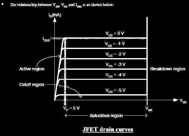
150 Applying KVL through base circuit we can write (I b + I C ) R C + I b R f + V be = V cc Diff. w. r. t. I C we get ( I b / I c ) = - R C / (R f + R C ) Therefore, S Ico (1+ β) 1+ [βr C /(R C + R f )] Which is less than (1+β), signifying better thermal stability 148
151 Merits: Circuit stabilizes the operating point against variations in temperature and β (i.e. replacement of transistor) Demerits: As β -value is fixed (and generally unknown) for a given transistor, this relation can be satisfied either by keeping Rc fairly large or making Rf very low. If Rc is large, a high Vcc is necessary, which increases cost as well as precautions necessary while handling. If Rf is low, the reverse bias of the collector base region is small, which limits the range of collector voltage swing that leaves the transistor in active mode. The resistor Rf causes an AC feedback, reducing the voltage gain of the amplifier. This undesirable effect is a trade-off for greater Q-point stability. Usage: The feedback also decreases the input impedance of the amplifier as seen from the base, which can be advantageous. Due to the gain reduction from feedback, this biasing form is used only when the trade-off for stability is warranted. 149
152 The Potential Divider Bias Circuit This is the most commonly used arrangement for biasing as it provide good bias stability. In this arrangement the emitter resistance RE provides stabilization. The resistance RE cause a voltage drop in a direction so as to reverse bias the emitter junction. Since the emitter-base junction is to be forward biased, the base voltage is obtained from R1-R2 network. The net forward bias across the emitter base junction is equal to VB- dc voltage drop across RE. The base voltage is set by Vcc and R1 and R2. The dc bias circuit is independent of transistor current gain. In case of amplifier, to avoid the loss of ac signal, a capacitor of large capacitance is connected across RE. The capacitor offers a very small reactance to ac signal and so it passes through the condensor. 150


153 The Potential Divider Bias Circuit VCC R 1 R 2 B VCC R C C E R E To find the stability of this circuit we have to convert this circuit into its Thevenin s Equivalent circuit R R *R th = 1 2 & V th = Vcc R 2 R 1 +R 2 R 1 +R 2 151

154 The Potential Divider Bias Circuit Thevenin Equivalent Ckt VCC Applying KVL through input base circuit we can write I b R Th + I E R E + V be = V Th Therefore, I b R Th + (I C + I b ) R E + V BE = V Th Diff. w. r. t. I C & rearranging we get R C ( I b / I c ) = - R E / (R Th + R E ) + _ I b RTh VTh I C C Therefore, 1 SIco B RE 1 IE E RE RE RTh This shows that S Ico is inversely proportional to R E and It is less than (1+β), signifying better thermal stability Thevenin Equivalent Voltage Self-bias Resistor 152
155 Merits: Operating point is almost independent of β variation. Operating point stabilized against shift in temperature. Demerits: As β-value is fixed for a given transistor, this relation can be satisfied either by keeping RE fairly large, or making R1 R2 very low. If RE is of large value, high VCC is necessary. This increases cost as well as precautions necessary while handling. If R1 R2 is low, either R1 is low, or R2 is low, or both are low. A low R1 raises VB closer to VC, reducing the available swing in collector voltage, and limiting how large RC can be made without driving the transistor out of active mode. A low R2 lowers Vbe, reducing the allowed collector current. Lowering both resistor values draws more current from the power supply and lowers the input resistance of the amplifier as seen from the base. AC as well as DC feedback is caused by RE, which reduces the AC voltage gain of the amplifier. A method to avoid AC feedback while retaining DC feedback is discussed below. Usage: The circuit's stability and merits as above make it widely used for linear circuits. 153
156 Summary The Q-point is the best point for operation of a transistor for a given collector current. The purpose of biasing is to establish a stable operating point (Q-point). The linear region of a transistor is the region of operation within saturation and cutoff. Out of all the biasing circuits, potential divider bias circuit provides highest stability to operating point. 154
157 Summary of Biasing Techniques
158 UNIT V Field Effect Transistor and FET Amplifiers


159 The Field Effect Transistor (FET) In 1945, Shockley had an idea for making a solid state device out of semiconductors. He reasoned that a strong electrical field could cause the flow of electricity within a nearby semiconductor. He tried to build one, but it didn't work. Three years later, Brattain & Bardeen built the first working transistor, the germanium point-contact transistor, which was designed as the junction (sandwich) transistor. In 1960 Bell scientist John Atalla developed a new design based on Shockley's original field-effect theories. By the late 1960s, manufacturers converted from junction type integrated circuits to field effect devices.


160 The Field Effect Transistor (FET) Field effect devices are those in which current is controlled by the action of an electron field, rather than carrier injection. Field-effect transistors are so named because a weak electrical signal coming in through one electrode creates an electrical field through the rest of the transistor. The FET was known as a unipolar transistor. The term refers to the fact that current is transported by carriers of one polarity (majority), whereas in the conventional bipolar transistor carriers of both polarities (majority and minority) are involved.
161 The Field Effect Transistor (FET) The family of FET devices may be divided into : Junction FET Depletion Mode MOSFET Enhancement Mode MOSFET

162 Junction FETs (JFETs) JFETs consists of a piece of high-resistivity semiconductor material (usually Si) which constitutes a channel for the majority carrier flow. Conducting semiconductor channel between two ohmic contacts source & drain

163 Junction FETs JFET is a high-input resistance device, while the BJT is comparatively low. If the channel is doped with a donor impurity, n-type material is formed and the channel current will consist of electrons. If the channel is doped with an acceptor impurity, p-type material will be formed and the channel current will consist of holes. N-channel devices have greater conductivity than p- channel types, since electrons have higher mobility than do holes; thus n-channel JFETs are approximately twice as efficient conductors compared to their p-channel counterparts.


164 Junction FETs (JFETs) The magnitude of this current is controlled by a voltage applied to a gate, which is a reverse-biased. The fundamental difference between JFET and BJT devices: when the JFET junction is reverse-biased the gate current is practically zero, whereas the base current of the BJT is always some value greater than zero.


165 Basic structure of JFETs In addition to the channel, a JFET contains two ohmic contacts: the source and the drain. The JFET will conduct current equally well in either direction and the source and drain leads are usually interchangeable.


")
166 Basic structure Source Gate p + G Drain Circuit symbol for n-channel FET S G D S n n-channel D p + Depletion region Cross section p + G n n S n-channel D Channel S G D p + Metal electrode Insulation Depletion n (SiO 2 regions ) n-channel p (b) thickness p + (a)
167 N-channel JFET This transistor is made by forming a channel of N-type material in a P-type substrate. Three wires are then connected to the device. One at each end of the channel. One connected to the substrate. In a sense, the device is a bit like a PN-junction diode, except that there are two wires connected to the N-type side.
168 How JFET Function The gate is connected to the source. Since the pn junction is reverse-biased, little current will flow in the gate connection. The potential gradient established will form a depletion layer, where almost all the electrons present in the n-type channel will be swept away. The most depleted portion is in the high field between the G and the D, and the least-depleted area is between the G and the S.
169 How JFET Function Because the flow of current along the channel from the (+ve) drain to the (-ve) source is really a flow of free electrons from S to D in the n-type Si, the magnitude of this current will fall as more Si becomes depleted of free electrons. There is a limit to the drain current (I D ) which increased V DS can drive through the channel. This limiting current is known as I DSS (Drain-to- Source current with the gate shorted to the source).


170 The output characteristics of an n-channel JFET with the gate short-circuited to the source. The initial rise in I D is related to the buildup of the depletion layer as V DS increases. The curve approaches the level of the limiting current I DSS when I D begins to be pinched off. The physical meaning of this term leads to one definition of pinch-off voltage, V P, which is the value of V DS at which the maximum I DSS flows.

171 With a steady gate-source voltage of 1 V there is always 1 V across the wall of the channel at the source end. A drain-source voltage of 1 V means that there will be 2 V across the wall at the drain end. (The drain is up 1V from the source potential and the gate is 1V down, hence the total difference is 2V.) The higher voltage difference at the drain end means that the electron channel is squeezed down a bit more at this end.

172 When the drain-source voltage is increased to 10V the voltage across the channel walls at the drain end increases to 11V, but remains just 1V at the source end. The field across the walls near the drain end is now a lot larger than at the source end. As a result the channel near the drain is squeezed down quite a lot.

173 Increasing the source-drain voltage to 20V squeezes down this end of the channel still more. As we increase this voltage we increase the electric field which drives electrons along the open part of the channel. However, also squeezes down the channel near the drain end. This reduction in the open channel width makes it harder for electrons to pass. As a result the drain-source current tends to remain constant when we increase the drain-source voltage.


174
175 Increasing V DS increases the widths of depletion layers, which penetrate more into channel and hence result in more channel narrowing toward the drain. The resistance of the n-channel, R AB therefore increases with V DS. The drain current: I DS = V DS /R AB I D versus V DS exhibits a sub linear behavior, see figure for V DS < 5V. The pinch-off voltage, V P is the magnitude of reverse bias needed across the p + n junction to make them just touch at the drain end. Since actual bias voltage across p + n junction at drain end is V GD, the pinch-off occur whenever: V GD = -V P.

176

177 Beyond V DS = V P, there is a short pinchoff channel of length, l po. As V DS increases, most of additional voltage simply drops across as this region is depleted of carriers and hence highly resistive. Voltage drop across channel length, L ch remain as V P. Beyond pinch-off then I D = V P /R AP (V DS >V P ).
.")

178 What happen when negative voltage, says V GS = -2V, is applied to gate with respect to source (with V DS =0). The p + n junction are now reverse biased from the start, the channel is narrower, and channel resistance is now larger than in the V GS = 0 case.
179 The drain current that flows when a small V DS applied (Fig b) is now smaller than in V GS = 0 case. Applied V DS = 3 V to pinch-off the channel (Fig c). When V DS = 3V, V GD across p + n junction at drain end is -5V, which is V P, so channel becomes pinch-off. Beyond pinch-off, I D is nearly saturated just as in the V GS =0 case. Pinch-off occurs at V DS = V DS(sat), V DS(sat) = V P +V GS, where V GS is ve voltage (reducing V P ). For V DS >V D(SAT), I D becomes nearly saturated at value as I DS.
180 Beyond pinch-of, with ve V GS, I DS is Where R AP (V GS ) is the effective resistance of the conducting n-channel from A to P, which depends on channel thickness and hence V GS. When V GS = -V P = -5V with V DS = 0, the two depletion layers touch over the entire channel length and the whole channel is closed. The channel said to be off.


181


182
183 There is a convenient relationship between I DS and V GS. Beyond pinch-off 2 V GS I DS I 1 DSS V GS (off ) Where IDSS is drain current when VGS= 0 and V GS(off) is defined as V P, that is gatesource voltage that just pinches off the channel. The pinch off voltage VP here is a +ve quantity because it was introduced through V DS(sat). V GS(off) however is negative, -V P.


184
185 I-V characteristics
186 I-V characteristics
187 JFET: I-V characteristics
188 The transconductance curve The process for plotting transconductance curve for a given JFET: Plot a point that corresponds to value of V GS(off). Plot that corresponds to value of I DSS. Select 3 or more values of V GS between 0 V and V GS(off). For value of V GS, determine the corresponding value of I D from Plot the point from (3) and connect all the plotted point with a smooth curve.
189
190 MOSFETs and Their Characteristics The metal-oxide semiconductor field effect transistor has a gate, source, and drain just like the JFET. The drain current in a MOSFET is controlled by the gate-source voltage V GS. There are two basic types of MOSFETS: the enhancement-type and the depletion-type. The enhancement-type MOSFET is usually referred to as an E-MOSFET, and the depletion-type, a D-MOSFET. The MOSFET is also referred to as an IGFET because the gate is insulated from the channel.
191 MOSFETs and Their Characteristics
192 MOSFETs and Their Characteristics
193 MOSFETs and Their Characteristics Fig (a) shows the construction of an n-channel, enhancement-type MOSFET. The p-type substrate makes contact with the SiO2 insulator. Because of this, there is no channel for conduction between the drain and source terminals.
194 Unijunction Transistor (UJT) Simple two layer transistor Operates using the principle of avalanche breakdown producing a saw tooth output Used to trigger an SCR or TRIAC Also used within pulse circuitry Output from photocells, thermistors, and other transducers can be used to trigger
195 Unijunction Transistor (UJT)
196 Silicon Controlled Rectifier (SCR)
197 SCR - Continued Three terminals anode - P-layer cathode - N-layer (opposite end) gate - P-layer near the cathode Three junctions - four layers Connect power such that the anode is positive with respect to the cathode - no current will flow NOTE: Blocked by the reverse bias of junction 2
198 SCR - Continued Positive potential applied to the gate Current will flow - TURNED-ON Once turned on, gate potential can be removed and the SCR still conducts CALLED LATCHING Holding current maintains latch
199 Silicon Controlled Rectifier
Chapter 3 Bipolar Junction Transistors (BJT)
") Chapter 3 Bipolar Junction Transistors (BJT) Transistors In analog circuits, transistors are used in amplifiers and linear regulated power supplies. In digital circuits they function as electrical switches,
Chapter 3 Bipolar Junction Transistors (BJT) Transistors In analog circuits, transistors are used in amplifiers and linear regulated power supplies. In digital circuits they function as electrical switches,
FET. Field Effect Transistors ELEKTRONIKA KONTROL. Eka Maulana, ST, MT, M.Eng. Universitas Brawijaya. p + S n n-channel. Gate. Basic structure.
 FET Field Effect Transistors ELEKTRONIKA KONTROL Basic structure Gate G Source S n n-channel Cross section p + p + p + G Depletion region Drain D Eka Maulana, ST, MT, M.Eng. Universitas Brawijaya S Channel
UNIT 3: FIELD EFFECT TRANSISTORS
 FIELD EFFECT TRANSISTOR: UNIT 3: FIELD EFFECT TRANSISTORS The field effect transistor is a semiconductor device, which depends for its operation on the control of current by an electric field. There are
UNIT 3 Transistors JFET
 UNIT 3 Transistors JFET Mosfet Definition of BJT A bipolar junction transistor is a three terminal semiconductor device consisting of two p-n junctions which is able to amplify or magnify a signal. It
Intrinsic Semiconductor
 Semiconductors Crystalline solid materials whose resistivities are values between those of conductors and insulators. Good electrical characteristics and feasible fabrication technology are some reasons
SUMMER 13 EXAMINATION Subject Code: Model Answer Page No: / N
 Important Instructions to examiners: 1) The answers should be examined by key words and not as word-to-word as given in the model answer scheme. 2) The model answer and the answer written by candidate
Module 04.(B1) Electronic Fundamentals
 Electronic Fundamentals") 1.1a. Semiconductors - Diodes. Module 04.(B1) Electronic Fundamentals Question Number. 1. What gives the colour of an LED?. Option A. The active element. Option B. The plastic it is encased in. Option
1.1a. Semiconductors - Diodes. Module 04.(B1) Electronic Fundamentals Question Number. 1. What gives the colour of an LED?. Option A. The active element. Option B. The plastic it is encased in. Option
SRM INSTITUTE OF SCIENCE AND TECHNOLOGY (DEEMED UNIVERSITY)
") SRM INSTITUTE OF SCIENCE AND TECHNOLOGY (DEEMED UNIVERSITY) QUESTION BANK I YEAR B.Tech (II Semester) ELECTRONIC DEVICES (COMMON FOR EC102, EE104, IC108, BM106) UNIT-I PART-A 1. What are intrinsic and
SRM INSTITUTE OF SCIENCE AND TECHNOLOGY (DEEMED UNIVERSITY) QUESTION BANK I YEAR B.Tech (II Semester) ELECTRONIC DEVICES (COMMON FOR EC102, EE104, IC108, BM106) UNIT-I PART-A 1. What are intrinsic and
Chapter Two "Bipolar Transistor Circuits"
 Chapter Two "Bipolar Transistor Circuits" 1.TRANSISTOR CONSTRUCTION:- The transistor is a three-layer semiconductor device consisting of either two n- and one p-type layers of material or two p- and one
Analog Electronics. Electronic Devices, 9th edition Thomas L. Floyd Pearson Education. Upper Saddle River, NJ, All rights reserved.
 Analog Electronics BJT Structure The BJT has three regions called the emitter, base, and collector. Between the regions are junctions as indicated. The base is a thin lightly doped region compared to the
Student Lecture by: Giangiacomo Groppi Joel Cassell Pierre Berthelot September 28 th 2004
 Student Lecture by: Giangiacomo Groppi Joel Cassell Pierre Berthelot September 28 th 2004 Lecture outline Historical introduction Semiconductor devices overview Bipolar Junction Transistor (BJT) Field
PHYS 3050 Electronics I
 PHYS 3050 Electronics I Chapter 4. Semiconductor Diodes and Transistors Earth, Moon, Mars, and Beyond Dr. Jinjun Shan, Associate Professor of Space Engineering Department of Earth and Space Science and
UNIT I - TRANSISTOR BIAS STABILITY
 UNIT I - TRANSISTOR BIAS STABILITY OBJECTIVE On the completion of this unit the student will understand NEED OF BIASING CONCEPTS OF LOAD LINE Q-POINT AND ITS STABILIZATION AND COMPENSATION DIFFERENT TYPES
KOM2751 Analog Electronics :: Dr. Muharrem Mercimek :: YTU - Control and Automation Dept. 1 2 (CONT D - II) DIODE APPLICATIONS
 DIODE APPLICATIONS") KOM2751 Analog Electronics :: Dr. Muharrem Mercimek :: YTU - Control and Automation Dept. 1 2 (CONT D - II) DIODE APPLICATIONS Most of the content is from the textbook: Electronic devices and circuit theory,
KOM2751 Analog Electronics :: Dr. Muharrem Mercimek :: YTU - Control and Automation Dept. 1 2 (CONT D - II) DIODE APPLICATIONS Most of the content is from the textbook: Electronic devices and circuit theory,
AE103 ELECTRONIC DEVICES & CIRCUITS DEC 2014
 Q.2 a. State and explain the Reciprocity Theorem and Thevenins Theorem. a. Reciprocity Theorem: If we consider two loops A and B of network N and if an ideal voltage source E in loop A produces current
EC6202-ELECTRONIC DEVICES AND CIRCUITS YEAR/SEM: II/III UNIT 1 TWO MARKS. 1. Define diffusion current.
 EC6202-ELECTRONIC DEVICES AND CIRCUITS YEAR/SEM: II/III UNIT 1 TWO MARKS 1. Define diffusion current. A movement of charge carriers due to the concentration gradient in a semiconductor is called process
UNIT-VI FIELD EFFECT TRANSISTOR. 1. Explain about the Field Effect Transistor and also mention types of FET s.
 UNIT-I FIELD EFFECT TRANSISTOR 1. Explain about the Field Effect Transistor and also mention types of FET s. The Field Effect Transistor, or simply FET however, uses the voltage that is applied to their
Shankersinh Vaghela Bapu Institute of Technology INDEX
 Shankersinh Vaghela Bapu Institute of Technology Diploma EE Semester III 3330905: ELECTRONIC COMPONENTS AND CIRCUITS INDEX Sr. No. Title Page Date Sign Grade 1 Obtain I-V characteristic of Diode. 2 To
Chapter 8. Field Effect Transistor
 Chapter 8. Field Effect Transistor Field Effect Transistor: The field effect transistor is a semiconductor device, which depends for its operation on the control of current by an electric field. There
Analog Electronic Circuits
 Analog Electronic Circuits Chapter 1: Semiconductor Diodes Objectives: To become familiar with the working principles of semiconductor diode To become familiar with the design and analysis of diode circuits
UNIT-I SEMICONDUCTOR DEVICES
 SEMICONDUCTOR MATERIALS: UNIT-I SEMICONDUCTOR DEVICES INSULATOR: An insulator is a material that offers a very low level of conductivity under Pressure from an applied voltage source. In this material
DEPARTMENT OF ELECTRONICS AND COMMUNICATION ENGINEERING III SEMESTER EC 6304 ELECTRONIC CIRCUITS I. (Regulations 2013)
") DEPARTMENT OF ELECTRONICS AND COMMUNICATION ENGINEERING III SEMESTER EC 6304 ELECTRONIC CIRCUITS I (Regulations 2013 UNIT-1 Part A 1. What is a Q-point? [N/D 16] The operating point also known as quiescent
DEPARTMENT OF ELECTRONICS AND COMMUNICATION ENGINEERING III SEMESTER EC 6304 ELECTRONIC CIRCUITS I (Regulations 2013 UNIT-1 Part A 1. What is a Q-point? [N/D 16] The operating point also known as quiescent
EE70 - Intro. Electronics
 EE70 - Intro. Electronics Course website: ~/classes/ee70/fall05 Today s class agenda (November 28, 2005) review Serial/parallel resonant circuits Diode Field Effect Transistor (FET) f 0 = Qs = Qs = 1 2π
Difference between BJTs and FETs. Junction Field Effect Transistors (JFET)
") Difference between BJTs and FETs Transistors can be categorized according to their structure, and two of the more commonly known transistor structures, are the BJT and FET. The comparison between BJTs
Difference between BJTs and FETs Transistors can be categorized according to their structure, and two of the more commonly known transistor structures, are the BJT and FET. The comparison between BJTs
EXPERIMENTS USING SEMICONDUCTOR DIODES
 EXPERIMENT 9 EXPERIMENTS USING SEMICONDUCTOR DIODES Semiconductor Diodes Structure 91 Introduction Objectives 92 Basics of Semiconductors Revisited 93 A p-n Junction Operation of a p-n Junction A Forward
 Code No: Y0221/R07 Set No. 1 I B.Tech Supplementary Examinations, Apr/May 2013 BASIC ELECTRONIC DEVICES AND CIRCUITS (Electrical & Electronics Engineering) Time: 3 hours Max Marks: 80 Answer any FIVE Questions
Lesson 5. Electronics: Semiconductors Doping p-n Junction Diode Half Wave and Full Wave Rectification Introduction to Transistors-
 Lesson 5 Electronics: Semiconductors Doping p-n Junction Diode Half Wave and Full Wave Rectification Introduction to Transistors- Types and Connections Semiconductors Semiconductors If there are many free
 Electronic Devices 1. Current flowing in each of the following circuits A and respectively are: (Circuit 1) (Circuit 2) 1) 1A, 2A 2) 2A, 1A 3) 4A, 2A 4) 2A, 4A 2. Among the following one statement is not
QUESTION BANK EC6201 ELECTRONIC DEVICES UNIT I SEMICONDUCTOR DIODE PART A. It has two types. 1. Intrinsic semiconductor 2. Extrinsic semiconductor.
 FATIMA MICHAEL COLLEGE OF ENGINEERING & TECHNOLOGY Senkottai Village, Madurai Sivagangai Main Road, Madurai - 625 020. [An ISO 9001:2008 Certified Institution] QUESTION BANK EC6201 ELECTRONIC DEVICES SEMESTER:
Bipolar Junction Transistors
 Bipolar Junction Transistors Invented in 1948 at Bell Telephone laboratories Bipolar junction transistor (BJT) - one of the major three terminal devices Three terminal devices more useful than two terminal
FIELD EFFECT TRANSISTOR (FET) 1. JUNCTION FIELD EFFECT TRANSISTOR (JFET)
 1. JUNCTION FIELD EFFECT TRANSISTOR (JFET)") FIELD EFFECT TRANSISTOR (FET) The field-effect transistor (FET) is a three-terminal device used for a variety of applications that match, to a large extent, those of the BJT transistor. Although there
FIELD EFFECT TRANSISTOR (FET) The field-effect transistor (FET) is a three-terminal device used for a variety of applications that match, to a large extent, those of the BJT transistor. Although there
Subject Code: Model Answer Page No: / N
 Important Instructions to examiners: 1) The answers should be examined by key words and not as word-to-word as given in the model answer scheme. 2) The model answer and the answer written by candidate
EDC UNIT IV- Transistor and FET JFET Characteristics EDC Lesson 4- ", Raj Kamal, 1
 EDC UNIT IV- Transistor and FET Characteristics Lesson-10: JFET Characteristics Qualitative Discussion 2008 EDC Lesson 4- ", Raj Kamal, 1 n-junction FET and p-jfet Symbols D D + D G + V DS V DS V GS S
Department of Electrical Engineering IIT Madras
 Department of Electrical Engineering IIT Madras Sample Questions on Semiconductor Devices EE3 applicants who are interested to pursue their research in microelectronics devices area (fabrication and/or
I E I C since I B is very small
 Figure 2: Symbols and nomenclature of a (a) npn and (b) pnp transistor. The BJT consists of three regions, emitter, base, and collector. The emitter and collector are usually of one type of doping, while
EDC UNIT IV- Transistor and FET Characteristics EDC Lesson 9- ", Raj Kamal, 1
 EDC UNIT IV- Transistor and FET Characteristics Lesson-9: JFET and Construction of JFET 2008 EDC Lesson 9- ", Raj Kamal, 1 1. Transistor 2008 EDC Lesson 9- ", Raj Kamal, 2 Transistor Definition The transferred-resistance
Diode and Bipolar Transistor Circuits
 Diode and Bipolar Transistor Circuits 2 2.1 A Brief Review of Semiconductors Semiconductors are crystalline structures in which each atom shares its valance electrons with the neighboring atoms. The simple
Unit III FET and its Applications. 2 Marks Questions and Answers
 Unit III FET and its Applications 2 Marks Questions and Answers 1. Why do you call FET as field effect transistor? The name field effect is derived from the fact that the current is controlled by an electric
UNIT II JFET, MOSFET, SCR & UJT
 UNIT II JFET, MOSFET, SCR & UJT JFET JFET as an Amplifier and its Output Characteristics JFET Applications MOSFET Working Principles, SCR Equivalent Circuit and V-I Characteristics. SCR as a Half wave
R a) Draw and explain VI characteristics of Si & Ge diode. (8M) b) Explain the operation of SCR & its characteristics (8M)
 Draw and explain VI characteristics of Si & Ge diode. (8M) b) Explain the operation of SCR & its characteristics (8M)") SET - 1 1. a) Define i) transient capacitance ii) Diffusion capacitance (4M) b) Explain Fermi level in intrinsic and extrinsic semiconductor (4M) c) Derive the expression for ripple factor of Half wave
SET - 1 1. a) Define i) transient capacitance ii) Diffusion capacitance (4M) b) Explain Fermi level in intrinsic and extrinsic semiconductor (4M) c) Derive the expression for ripple factor of Half wave
FIELD EFFECT TRANSISTORS MADE BY : GROUP (13)/PM
/PM") FIELD EFFECT TRANSISTORS MADE BY : GROUP (13)/PM THE FIELD EFFECT TRANSISTOR (FET) In 1945, Shockley had an idea for making a solid state device out of semiconductors. He reasoned that a strong electrical
FIELD EFFECT TRANSISTORS MADE BY : GROUP (13)/PM THE FIELD EFFECT TRANSISTOR (FET) In 1945, Shockley had an idea for making a solid state device out of semiconductors. He reasoned that a strong electrical
Field Effect Transistors (npn)
") Field Effect Transistors (npn) gate drain source FET 3 terminal device channel e - current from source to drain controlled by the electric field generated by the gate base collector emitter BJT 3 terminal
Field Effect Transistors (npn) gate drain source FET 3 terminal device channel e - current from source to drain controlled by the electric field generated by the gate base collector emitter BJT 3 terminal
SYED AMMAL ENGINEERING COLLEGE
 SYED AMMAL ENGINEERING COLLEGE (Approved by the AICTE, New Delhi, Govt. of Tamilnadu and Affiliated to Anna University, Chennai) Established in 1998 - An ISO 9001:2008 Certified Institution Dr. E.M.Abdullah
Electronic Circuits I. Instructor: Dr. Alaa Mahmoud
 Electronic Circuits I Instructor: Dr. Alaa Mahmoud alaa_y_emam@hotmail.com Chapter 27 Diode and diode application Outline: Semiconductor Materials The P-N Junction Diode Biasing P-N Junction Volt-Ampere
Figure1: Basic BJT construction.
 Chapter 4: Bipolar Junction Transistors (BJTs) Bipolar Junction Transistor (BJT) Structure The BJT is constructed with three doped semiconductor regions separated by two pn junctions, as in Figure 1(a).
Scheme Q.1 Attempt any SIX of following: 12-Total Marks a) Draw symbol NPN and PNP transistor. 2 M Ans: Symbol Of NPN and PNP BJT (1M each)
 Draw symbol NPN and PNP transistor. 2 M Ans: Symbol Of NPN and PNP BJT (1M each)") Q. No. WINTER 16 EXAMINATION (Subject Code: 17319) Model Answer Important Instructions to examiners: 1) The answers should be examined by key words and not as word-to-word as given in the model answer
Q. No. WINTER 16 EXAMINATION (Subject Code: 17319) Model Answer Important Instructions to examiners: 1) The answers should be examined by key words and not as word-to-word as given in the model answer
Basic Electronics: Diodes and Transistors. October 14, 2005 ME 435
 Basic Electronics: Diodes and Transistors Eşref Eşkinat E October 14, 2005 ME 435 Electric lectricity ity to Electronic lectronics Electric circuits are connections of conductive wires and other devices
UNIT 4 BIASING AND STABILIZATION
 UNIT 4 BIASING AND STABILIZATION TRANSISTOR BIASING: To operate the transistor in the desired region, we have to apply external dec voltages of correct polarity and magnitude to the two junctions of the
Reg. No. : Question Paper Code : B.E./B.Tech. DEGREE EXAMINATION, NOVEMBER/DECEMBER Second Semester
 WK 5 Reg. No. : Question Paper Code : 27184 B.E./B.Tech. DEGREE EXAMINATION, NOVEMBER/DECEMBER 2015. Time : Three hours Second Semester Electronics and Communication Engineering EC 6201 ELECTRONIC DEVICES
1) A silicon diode measures a low value of resistance with the meter leads in both positions. The trouble, if any, is
 A silicon diode measures a low value of resistance with the meter leads in both positions. The trouble, if any, is") 1) A silicon diode measures a low value of resistance with the meter leads in both positions. The trouble, if any, is A [ ]) the diode is open. B [ ]) the diode is shorted to ground. C [v]) the diode is
1) A silicon diode measures a low value of resistance with the meter leads in both positions. The trouble, if any, is A [ ]) the diode is open. B [ ]) the diode is shorted to ground. C [v]) the diode is
Section:A Very short answer question
 Section:A Very short answer question 1.What is the order of energy gap in a conductor, semi conductor, and insulator?. Conductor - no energy gap Semi Conductor - It is of the order of 1 ev. Insulator -
Ch5 Diodes and Diodes Circuits
 Circuits and Analog Electronics Ch5 Diodes and Diodes Circuits 5.1 The Physical Principles of Semiconductor 5.2 Diodes 5.3 Diode Circuits 5.4 Zener Diode References: Floyd-Ch2; Gao-Ch6; 5.1 The Physical
Paper-1 (Circuit Analysis) UNIT-I
 UNIT-I") Paper-1 (Circuit Analysis) UNIT-I AC Fundamentals & Kirchhoff s Current and Voltage Laws 1. Explain how a sinusoidal signal can be generated and give the significance of each term in the equation? 2. Define
Paper-1 (Circuit Analysis) UNIT-I AC Fundamentals & Kirchhoff s Current and Voltage Laws 1. Explain how a sinusoidal signal can be generated and give the significance of each term in the equation? 2. Define
Power Semiconductor Devices
 TRADEMARK OF INNOVATION Power Semiconductor Devices Introduction This technical article is dedicated to the review of the following power electronics devices which act as solid-state switches in the circuits.
UNIT-1 Bipolar Junction Transistors. Text Book:, Microelectronic Circuits 6 ed., by Sedra and Smith, Oxford Press
 UNIT-1 Bipolar Junction Transistors Text Book:, Microelectronic Circuits 6 ed., by Sedra and Smith, Oxford Press Figure 6.1 A simplified structure of the npn transistor. Microelectronic Circuits, Sixth
NAME: Last First Signature
 UNIVERSITY OF CALIFORNIA, BERKELEY College of Engineering Department of Electrical Engineering and Computer Sciences EE 130: IC Devices Spring 2003 FINAL EXAMINATION NAME: Last First Signature STUDENT
CENTURION UNIVERSITY OF TECHNOLOGY AND MANAGEMENT SCHOOL OF ENGINEERING & TECHNOLOGYDEPARTMENT OF ELECTRONICS & COMMUNICATION ENGINEERING
 CENTURION UNIVERSITY OF TECHNOLOGY AND MANAGEMENT SCHOOL OF ENGINEERING & TECHNOLOGYDEPARTMENT OF ELECTRONICS & COMMUNICATION ENGINEERING ELECTRONIC DEVICES Section: ECE SEM: II PART-A 1. a) In a N-type
MODULE-2: Field Effect Transistors (FET)
") FORMAT-1B Definition: MODULE-2: Field Effect Transistors (FET) FET is a three terminal electronic device used for variety of applications that match with BJT. In FET, an electric field is established by
FORMAT-1B Definition: MODULE-2: Field Effect Transistors (FET) FET is a three terminal electronic device used for variety of applications that match with BJT. In FET, an electric field is established by
MAHARASHTRA STATE BOARD OF TECHNICAL EDUCATION (Autonomous) (ISO/IEC Certified) MODEL ANSWER
 (ISO/IEC Certified) MODEL ANSWER") Important Instructions to examiners: 1) The answers should be examined by key words and not as word-to-word as given in the model answer scheme. 2) The model answer and the answer written by candidate
Important Instructions to examiners: 1) The answers should be examined by key words and not as word-to-word as given in the model answer scheme. 2) The model answer and the answer written by candidate
Solid State Devices- Part- II. Module- IV
 Solid State Devices- Part- II Module- IV MOS Capacitor Two terminal MOS device MOS = Metal- Oxide- Semiconductor MOS capacitor - the heart of the MOSFET The MOS capacitor is used to induce charge at the
Review Energy Bands Carrier Density & Mobility Carrier Transport Generation and Recombination
 Review Energy Bands Carrier Density & Mobility Carrier Transport Generation and Recombination Current Transport: Diffusion, Thermionic Emission & Tunneling For Diffusion current, the depletion layer is
Module 2. B.Sc. I Electronics. Developed by: Mrs. Neha S. Joshi Asst. Professor Department of Electronics Willingdon College, Sangli
 Module 2 B.Sc. I Electronics Developed by: Mrs. Neha S. Joshi Asst. Professor Department of Electronics Willingdon College, Sangli BIPOLAR JUNCTION TRANSISTOR SCOPE OF THE CHAPTER- This chapter introduces
(a) BJT-OPERATING MODES & CONFIGURATIONS
 BJT-OPERATING MODES & CONFIGURATIONS") (a) BJT-OPERATING MODES & CONFIGURATIONS 1. The leakage current I CBO flows in (a) The emitter, base and collector leads (b) The emitter and base leads. (c) The emitter and collector leads. (d) The base
(a) BJT-OPERATING MODES & CONFIGURATIONS 1. The leakage current I CBO flows in (a) The emitter, base and collector leads (b) The emitter and base leads. (c) The emitter and collector leads. (d) The base
Basic Electronics. Introductory Lecture Course for. Technology and Instrumentation in Particle Physics Chicago, Illinois June 9-14, 2011
 Basic Electronics Introductory Lecture Course for Technology and Instrumentation in Particle Physics 2011 Chicago, Illinois June 9-14, 2011 Presented By Gary Drake Argonne National Laboratory Session 3
Physics 160 Lecture 5. R. Johnson April 13, 2015
 Physics 160 Lecture 5 R. Johnson April 13, 2015 Half Wave Diode Rectifiers Full Wave April 13, 2015 Physics 160 2 Note that there is no ground connection on this side of the rectifier! Output Smoothing
FREQUENTLY ASKED QUESTIONS
 FREQUENTLY ASKED QUESTIONS UNIT-1 SUBJECT : ELECTRONIC DEVICES AND CIRCUITS SUBJECT CODE : EC6202 BRANCH: EEE PART -A 1. What is meant by diffusion current in a semi conductor? (APR/MAY 2010, 2011, NOV/DEC
TRANSISTOR BIASING AND STABILIZATION
 TRANSISTOR BIASING AND STABILIZATION 4.1 NEED FOR TRANSISTOR BIASING: If the o/p signal must be a faithful reproduction of the i/p signal, the transistor must be operated in active region. That means an
MTLE-6120: Advanced Electronic Properties of Materials. Semiconductor transistors for logic and memory. Reading: Kasap
 MTLE-6120: Advanced Electronic Properties of Materials 1 Semiconductor transistors for logic and memory Reading: Kasap 6.6-6.8 Vacuum tube diodes 2 Thermionic emission from cathode Electrons collected
MAHARASHTRA STATE BOARD OF TECHNICAL EDUCATION (Autonomous) (ISO/IEC Certified) Summer 2016 EXAMINATIONS.
 (ISO/IEC Certified) Summer 2016 EXAMINATIONS.") Summer 2016 EXAMINATIONS Subject Code: 17321 Model Answer Important Instructions to examiners: 1) The answers should be examined by key words and not as word-to-word as given in the answer scheme. 2) The
Summer 2016 EXAMINATIONS Subject Code: 17321 Model Answer Important Instructions to examiners: 1) The answers should be examined by key words and not as word-to-word as given in the answer scheme. 2) The
CHAPTER 1 DIODE CIRCUITS. Semiconductor act differently to DC and AC currents
 CHAPTER 1 DIODE CIRCUITS Resistance levels Semiconductor act differently to DC and AC currents There are three types of resistances 1. DC or static resistance The application of DC voltage to a circuit
Summer 2015 Examination. 1) The answers should be examined by key words and not as word-to-word as given in the model answer scheme.
 The answers should be examined by key words and not as word-to-word as given in the model answer scheme.") Summer 2015 Examination Subject Code: 17213 Model Answer Important Instructions to examiners: 1) The answers should be examined by key words and not as word-to-word as given in the model answer scheme.
Summer 2015 Examination Subject Code: 17213 Model Answer Important Instructions to examiners: 1) The answers should be examined by key words and not as word-to-word as given in the model answer scheme.
Basic Electronics Prof. Dr. Chitralekha Mahanta Department of Electronics and Communication Engineering Indian Institute of Technology, Guwahati
 Basic Electronics Prof. Dr. Chitralekha Mahanta Department of Electronics and Communication Engineering Indian Institute of Technology, Guwahati Module: 2 Bipolar Junction Transistors Lecture-1 Transistor
WINTER 14 EXAMINATION. Model Answer. 1) The answers should be examined by key words and not as word-to-word as given in the
 The answers should be examined by key words and not as word-to-word as given in the") WINTER 14 EXAMINATION Subject Code: 17213 Model Answer Important Instructions to examiners: 1) The answers should be examined by key words and not as word-to-word as given in the model answer scheme. 2)
WINTER 14 EXAMINATION Subject Code: 17213 Model Answer Important Instructions to examiners: 1) The answers should be examined by key words and not as word-to-word as given in the model answer scheme. 2)
INSTITUTE OF AERONAUTICAL ENGINEERING (Autonomous) Dundigal, Hyderabad
 Dundigal, Hyderabad") INSTITUTE OF AERONAUTICAL ENGINEERING (Autonomous) Dundigal, Hyderabad -500 043 COMPUTER SCIENCE AND ENGINEERING TUTORIAL QUESTION BANK Course Name : ELECTRONIC DEVICES AND CIRCUITS Course Code : A30404
INSTITUTE OF AERONAUTICAL ENGINEERING (Autonomous) Dundigal, Hyderabad -500 043 COMPUTER SCIENCE AND ENGINEERING TUTORIAL QUESTION BANK Course Name : ELECTRONIC DEVICES AND CIRCUITS Course Code : A30404
FET(Field Effect Transistor)
") Field Effect Transistor: Construction and Characteristic of JFETs. Transfer Characteristic. CS,CD,CG amplifier and analysis of CS amplifier MOSFET (Depletion and Enhancement) Type, Transfer Characteristic,
Field Effect Transistor: Construction and Characteristic of JFETs. Transfer Characteristic. CS,CD,CG amplifier and analysis of CS amplifier MOSFET (Depletion and Enhancement) Type, Transfer Characteristic,
Section 2.3 Bipolar junction transistors - BJTs
 Section 2.3 Bipolar junction transistors - BJTs Single junction devices, such as p-n and Schottkty diodes can be used to obtain rectifying I-V characteristics, and to form electronic switching circuits
7. Bipolar Junction Transistor
 41 7. Bipolar Junction Transistor 7.1. Objectives - To experimentally examine the principles of operation of bipolar junction transistor (BJT); - To measure basic characteristics of n-p-n silicon transistor
SETH JAI PARKASH POLYTECHNIC, DAMLA
 SETH JAI PARKASH POLYTECHNIC, DAMLA NAME OF FACULTY----------SANDEEP SHARMA DISCIPLINE---------------------- E.C.E (S.F) SEMESTER-------------------------2 ND SUBJECT----------------------------BASIC ELECTRONICS
EDC Lecture Notes UNIT-1
 P-N Junction Diode EDC Lecture Notes Diode: A pure silicon crystal or germanium crystal is known as an intrinsic semiconductor. There are not enough free electrons and holes in an intrinsic semi-conductor
F.Y. Diploma : Sem. II [DE/EJ/IE/IS/EE/MU/ET/EN/EX] Basic Electronics
![F.Y. Diploma : Sem. II [DE/EJ/IE/IS/EE/MU/ET/EN/EX] Basic Electronics](/thumbs/95/124107511.jpg "F.Y. Diploma : Sem. II [DE/EJ/IE/IS/EE/MU/ET/EN/EX] Basic Electronics") F.Y. Diploma : Sem. II [DE/EJ/IE/IS/EE/MU/ET/EN/EX] Basic Electronics Time: 3 Hrs.] Prelim Question Paper Solution [Marks : 70 Q.1 Attempt any FIE of the following : [10] Q.1(a) Draw the symbols for (i)
F.Y. Diploma : Sem. II [DE/EJ/IE/IS/EE/MU/ET/EN/EX] Basic Electronics Time: 3 Hrs.] Prelim Question Paper Solution [Marks : 70 Q.1 Attempt any FIE of the following : [10] Q.1(a) Draw the symbols for (i)
JFET 101, a Tutorial Look at the Junction Field Effect Transistor 8May 2007, edit 2April2016, Wes Hayward, w7zoi
 JFET 101, a Tutorial Look at the Junction Field Effect Transistor 8May 2007, edit 2April2016, Wes Hayward, w7zoi FETs are popular among experimenters, but they are not as universally understood as the
4.2.2 Metal Oxide Semiconductor Field Effect Transistor (MOSFET)
") 4.2.2 Metal Oxide Semiconductor Field Effect Transistor (MOSFET) The Metal Oxide Semitonductor Field Effect Transistor (MOSFET) has two modes of operation, the depletion mode, and the enhancement mode.
4.2.2 Metal Oxide Semiconductor Field Effect Transistor (MOSFET) The Metal Oxide Semitonductor Field Effect Transistor (MOSFET) has two modes of operation, the depletion mode, and the enhancement mode.
EIE209 Basic Electronics. Transistor Devices. Contents BJT and FET Characteristics Operations. Prof. C.K. Tse: T ransistor devices
 EIE209 Basic Electronics Transistor Devices Contents BJT and FET Characteristics Operations 1 What is a transistor? Three-terminal device whose voltage-current relationship is controlled by a third voltage
Downloaded from
 SOLID AND SEMICONDUCTOR DEVICES (EASY AND SCORING TOPIC) 1. Distinction of metals, semiconductor and insulator on the basis of Energy band of Solids. 2. Types of Semiconductor. 3. PN Junction formation
Table of Contents. iii
 Table of Contents Subject Page Experiment 1: Diode Characteristics... 1 Experiment 2: Rectifier Circuits... 7 Experiment 3: Clipping and Clamping Circuits 17 Experiment 4: The Zener Diode 25 Experiment
BJT. Bipolar Junction Transistor BJT BJT 11/6/2018. Dr. Satish Chandra, Assistant Professor, P P N College, Kanpur 1
 BJT Bipolar Junction Transistor Satish Chandra Assistant Professor Department of Physics P P N College, Kanpur www.satish0402.weebly.com The Bipolar Junction Transistor is a semiconductor device which
ELECTRONIC DEVICES AND CIRCUITS
 ELECTRONIC DEVICES AND CIRCUITS 1. As compared to a full wave rectifier using 2 diodes, the four diode bridge rectifier has the dominant advantage of (a) Higher current carrying (b) lower peak inverse
13. SEMICONDUCTOR DEVICES
 Synopsis: 13. SEMICONDUCTOR DEVICES 1. Solids are classified into two categories. a) Crystalline solids b) Amorphous solids 2. Crystalline solids : Crystalline solids have orderly arrangement of atoms
MAHARASHTRA STATE BOARD OF TECHNICAL EDUCATION (Autonomous) (ISO/IEC Certified) Subject Code: Model Answer Page No: 1/
 (ISO/IEC Certified) Subject Code: Model Answer Page No: 1/") MAHARASHTRA STATE BOARD OF TECHNICAL EDUCATION (Autonomous) (ISO/IEC 27001 2005 Certified) SUMMER 13 EXAMINATION Subject Code: 12025 Model Answer Page No: 1/ Important Instructions to examiners: 1) The
MAHARASHTRA STATE BOARD OF TECHNICAL EDUCATION (Autonomous) (ISO/IEC 27001 2005 Certified) SUMMER 13 EXAMINATION Subject Code: 12025 Model Answer Page No: 1/ Important Instructions to examiners: 1) The
Chapter Semiconductor Electronics
 Chapter Semiconductor Electronics Q1. p-n junction is said to be forward biased, when [1988] (a) the positive pole of the battery is joined to the p- semiconductor and negative pole to the n- semiconductor
Q1 A) Attempt any six: i) Draw the neat symbol of N-channel and P-channel FET
 Attempt any six: i) Draw the neat symbol of N-channel and P-channel FET") Subject Code:17319 Model Answer Page1 of 27 Important Instructions to examiners: 1) The answers should be examined by key words and not as word-to-word as given in the model answer scheme. 2) The model
Subject Code:17319 Model Answer Page1 of 27 Important Instructions to examiners: 1) The answers should be examined by key words and not as word-to-word as given in the model answer scheme. 2) The model
ELECTRONIC DEVICES AND CIRCUITS
 ELECTRONIC DEVICES AND CIRCUITS 1. At room temperature the current in an intrinsic semiconductor is due to A. holes B. electrons C. ions D. holes and electrons 2. Work function is the maximum energy required
VALLIAMMAI ENGINEERING COLLEGE SRM Nagar, Kattankulathur
 VALLIAMMAI ENGINEERING COLLEGE SRM Nagar, Kattankulathur 603 203. DEPARTMENT OF ELECTRONICS & COMMUNICATION ENGINEERING SUBJECT QUESTION BANK : EC6201 ELECTRONIC DEVICES SEM / YEAR: II / I year B.E.ECE
Three Terminal Devices
 Three Terminal Devices - field effect transistor (FET) - bipolar junction transistor (BJT) - foundation on which modern electronics is built - active devices - devices described completely by considering
This tutorial will suit all beginners who want to learn the fundamental concepts of transistors and transistor amplifier circuits.
 About the Tutorial An electronic signal contains some information which cannot be utilized if doesn t have proper strength. The process of increasing the signal strength is called as Amplification. Almost
Questions on JFET: 1) Which of the following component is a unipolar device?
 Which of the following component is a unipolar device?") Questions on JFET: 1) Which of the following component is a unipolar device? a) BJT b) FET c) DJT d) EFT 2) Current Conduction in FET takes place due e) Majority charge carriers only f) Minority charge
Questions on JFET: 1) Which of the following component is a unipolar device? a) BJT b) FET c) DJT d) EFT 2) Current Conduction in FET takes place due e) Majority charge carriers only f) Minority charge
 SEMICONDUCTOR EECTRONICS MATERIAS, DEVICES AND SIMPE CIRCUITS Important Points: 1. In semiconductors Valence band is almost filled and the conduction band is almost empty. The energy gap is very small
KOM2751 Analog Electronics :: Dr. Muharrem Mercimek :: YTU - Control and Automation Dept. 1 1 (CONT D) DIODES
 DIODES") KOM2751 Analog Electronics :: Dr. Muharrem Mercimek :: YTU - Control and Automation Dept. 1 1 (CONT D) DIODES Most of the content is from the textbook: Electronic devices and circuit theory, Robert L.
KOM2751 Analog Electronics :: Dr. Muharrem Mercimek :: YTU - Control and Automation Dept. 1 1 (CONT D) DIODES Most of the content is from the textbook: Electronic devices and circuit theory, Robert L.
Lecture 3: Transistors
 Lecture 3: Transistors Now that we know about diodes, let s put two of them together, as follows: collector base emitter n p n moderately doped lightly doped, and very thin heavily doped At first glance,
Basic Electronics Prof. Dr. Chitralekha Mahanta Department of Electronics and Communication Engineering Indian Institute of Technology, Guwahati
 Basic Electronics Prof. Dr. Chitralekha Mahanta Department of Electronics and Communication Engineering Indian Institute of Technology, Guwahati Module: 3 Field Effect Transistors Lecture-7 High Frequency