Basic Electronics: Diodes and Transistors. October 14, 2005 ME 435
|
|
|
- Elisabeth Ferguson
- 5 years ago
- Views:
Transcription
1 Basic Electronics: Diodes and Transistors Eşref Eşkinat E October 14, 2005 ME 435
2 Electric lectricity ity to Electronic lectronics Electric circuits are connections of conductive wires and other devices whereby the uniform flow of electrons occurs. Electronic circuits add a new dimension to electric circuits in that some means of control is exerted over the flow of electrons by another electrical signal, either a flow of electrons by another electrical signal, either a voltage or a current. Electronics technology experienced a revolution in 1948 with the invention of the transistor. Transistors control the flow of electrons through solid semiconductor substances. T solid-state state electronics.. Transistor technology is often referred to as
3 Active versus passive devices Active versus passive devices An active device is any type of circuit component with the ability to electrically control electron flow (electricity controlling electricity). In order for a circuit to be properly called electronic,, it must contain at least one active device. Components incapable of controlling current by means of another electrical signal are called passive devices. Resistors, capacitors, inductors, transformers, and even diodes are all passive devices. Active devices include, vacuum tubes, transistors, silicon-controlled rectifiers ( controlled rectifiers (SCRs SCRs), and TRIAC s
4 Amplifiers The practical benefit of active devices is their amplifying ability. An n active device allows a small amount of electricity to control a large amount of electricity. Devices utilizing a voltage as the controlling signal are called voltage- controlled devices. Devices working on the principle of one current controlling another current are known as current-controlled controlled devices.

5 Semiconductors Semiconductors have had a monumental impact. You find semiconductors at the heart of microprocessor chips as well as transistors. Anything that's computerized or uses radio waves depends on semiconductors. Today, most semiconductor chips and transistors are created with silicon.. You may have heard expressions like "Silicon Valley" and the "silicon economy," and that's why -- silicon is the heart of any electronic device. Clockwise from top: A chip, an LED and a transistor are all made from semiconductor material.
6 Understanding Silicon Understanding Silicon Silicon is a very common element.. It I t is the main element in sand. Silicon ilicon" " in the periodic table, is next to Aluminum luminum,, below carbon and above germanium. Carbon, silicon and germanium have a unique property in their electron structure -- each has four electrons in its outer orbital.. This allows them to form nice crystals. The four electrons form perfect covalent bonds with four neighboring atoms, creating a lattice.. In carbon, we know the crystalline form as diamond. In silicon, the crystalline form is a silvery, metallic- looking substance. Metals tend to be good conductors of electricity because they usually have "free electrons" that can move easily between atoms, and electricity involves the flow of electrons. All of the outer electrons in a silicon crystal are involved in perfect covalent bonds,, so they can't move around. A pure silicon crystal is nearly an insulator
7 Doping Silicon Doping Silicon You can change the behavior of silicon and turn it into a conductor by doping an impurity into the silicon crystal. N-type - In N-type N doping, phosphorus or arsenic is added to the silicon in small quantities. Phosphorus and arsenic each have five outer electrons. The fifth electron has nothing to bond to, so it's free to move around. N-type N silicon is a good conductor. Electrons have a negative charge, hence the name N-type. doping it. In doping, you mix a small amount of P-type - In P-type P doping, boron or gallium is the dopant. Boron and gallium each have only three outer electrons. When mixed into the silicon lattice, they form "holes" in the lattice where a silicon electron has nothing to bond to. The absence of an electron creates the effect of a positive charge, hence the name P-type. P Holes can conduct current. A hole accepts an electron from a neighbor, moving the hole over a space. P-type P silicon is a good conductor. N-type and P-type P silicon are not that amazing by themselves; but when you put them together, you get some very interesting behavior at the junction.
8 P-N N Junction The free electrons in the N-type silicon are repelled by the negative terminal of the battery. The holes in the P-type silicon are repelled by the positive terminal. At the junction between the N-type and P- type silicon, holes and free electrons meet. The electrons fill the holes. Those holes and free electrons cease to exist, and new holes and electrons spring up to take their place. The effect is that current flows through the junction. The negative electrons in the N-type silicon get attracted to the positive terminal of the battery. The positive holes in the P-type silicon get attracted to the negative terminal of the battery. No current flows across the junction because the holes and the electrons are each moving in the wrong direction.

9 Junction Diodes Junction Diodes A PN junction passes current only in one direction. A diode is an electrical device allowing current to move through it in one direction with far greater ease than in the other.
10 Diode Operation Diode Operation When the diode is forward- biased and conducting current, there is a small voltage dropped across it, leaving most of the battery voltage dropped across the lamp. When the battery's polarity is reversed and the diode becomes reverse- biased, it drops all of the battery's voltage and leaves none for the lamp.
11 Diode Characteristic Curve Diode Characteristic Curve A real diode requires about 0.7 V to enable significant current flow.
12 Review A diode is an electrical component acting as a one-way valve for current. When voltage is applied across a diode in such a way that the diode allows current, the diode is said to be forward forward-biased biased. When voltage is applied across a diode in such a way that the diode prohibits current, the diode is said to be reverse-biased biased. The voltage dropped across a conducting, forward-biased diode is called the forward voltage.. Forward voltage for a diode varies only slightly for changes in forward current and temperature, and is fixed principally by the chemical composition of the P-N P junction. Silicon diodes have a forward voltage of approximately 0.7 volts
13 Half Wave Rectifier Circuit Half Wave Rectifier Circuit Application : Light dimming When V i is positive, diode is reverse biased and is equivalent to open circuit. Therefore V 0 =V i. When Vi is negative, diode is forward biased and is equivalent to short circuit. Therefore V 0 =0 V.
14 Full Wave Rectifier Full Wave Rectifier If we need to rectify AC power so as to obtain the full use of both half-cycles of the sine wave, a different rectifier circuit configuration must be used. Such a circuit is called a full-wave rectifier.
15 Full rectifier Full rectifier

16 Inductive Kick Inductive Kick The switch attempts to change the current instantaneously. Inductors generate voltage to oppose current changes. The diode allows the voltage to dissipate through the resistor.
17 without Flyback diode Flyback diode with
18 Peak Detector Peak Detector When a time varying signal V in is applied at the input, the output V out retains the maximum positive value of the input signal. In the actual circuit there is some decrease of Vout in time because of the capacitor leakage.
19 Zener Diodes Zener Diodes When a diode is reverse biased with large voltage, it allows a large reverse current to flow : Breakdown. Special diodes with well defined breakdown voltages maintain constant voltage over a wide range of currents. They are Zener diodes and used as voltage regulators. Zener diode should be reverse biased with a voltage in excess of its zener voltage V z. Typically : V z = V.
20 Zener Diode as Voltage regulator Zener Diode as Voltage regulator In the above circuit, output voltage of the source, V z, is kept relatively constant, because of the breakdown characteristic of the Zener diode. Zener diodes are often rated by their power dissipation, which is: P Zmax = i Zmax V Z
21 Optoelectronic diodes Optoelectronic diodes Light emitting diode : LED Photodiode light detector circuit.

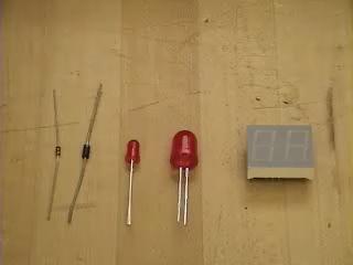
22 LED (Light Emitting Diodes) LED (Light Emitting Diodes) While all diodes release light, most don't do it very effectively. In an ordinary diode, the semiconductor material itself ends up absorbing a lot of the light energy. LEDs are specially constructed to release a large number of photons outward. of photons outward. LED LED s form the numbers on digital clocks,, transmit information from remote controls,, light up watches and tell you when your appliances are turned on. Collected together, they can form images on a jumbo television screen or illuminate a traffic light.
23 Diode Video Diode Video
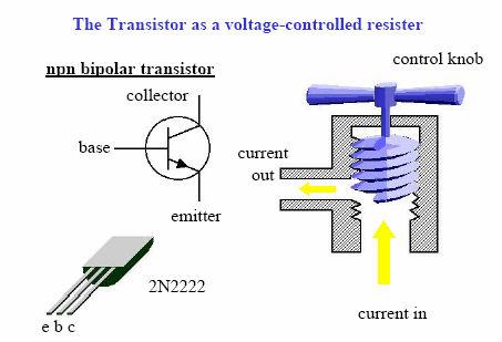
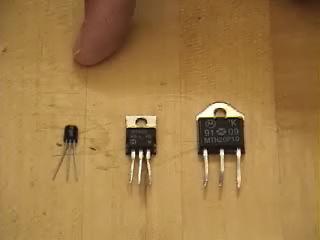
24 Transistors and Chips Transistors and Chips A transistor is created by using three layers rather than the two layers used in a diode. You can create either an NPN or a PNP sandwich. A transistor can act as a switch or an amplifier you apply a small current to the center layer of the sandwich, a much larger current can flow through the sandwich as a whole. This gives a transistor its switching behavior. A small current A transistor can act as a switch or an amplifier. When can turn a larger current on and off. A silicon chip is a piece of silicon that can hold thousands of transistors. With transistors acting as switches, you can create Boolean gates,, and with Boolean gates you can create microprocessor chips. The natural progression from silicon to doped silicon to transistors to chips is what has made microprocessors and other electronic devices so inexpensive. The fundamental principles are surprisingly simple. Today oday,, tens of millions of transistors can be inexpensively formed onto a single chip.
25 Transistors Transistors consist of multiple layers of Transistors consist of multiple layers of n- and p- silicon, examples are npn configuration or a pnp configuration in the bipolar junction transistor (BJT). A small amount of current introduced at the base (center) of the transistor will cause the overall device to be forward biased and allow current rent to flow from collector to emitter October 14, 2005 ME 435
26
27 BJT Transistor (NPN) BJT Transistor (NPN) I E =I C +I B V BE = V B -V E V CE = V C -V E V C > V B > V E I C = β I B Typically β 100.
28 Transistor Video Transistor Video
29 Simple Transistor Application Simple Transistor Application +10V Mechanical Switch Lamp 1K 10V 0.1A
30 Example Applications Example Applications
31 Characteristics of a common emitter Characteristics of a common emitter NPN BJT Cutoff : V BE < 0.7 V, i B =0 i C 0, V CE > 0. Active : V BE = 0.7 V i C =βi B, V CE > 0.7 V Saturation : i B >i C /β and V BE = 0.7 V V CE = V SAT = 0.2 V.
32 Power dissipation in Transistors Power dissipation in Transistors
33 The common emitter transistor circuit for a npn transistor. The transistor is forward biased when the base-to to-emitter voltage is V. When designing a transistor switch, the transistor must be in saturation when it is on (otherwise it will heat up and might fail) For BJT s,, the V CE at saturation is about 0.2V.2V. I C R C I B + - V BE - + V CE
34 Guaranteeing that the transistor is in saturation Guaranteeing that the transistor is in saturation Given a typical signal transistor, 2N3904 specifications : Max. collector current, I C (max) = 200mA, V CE at saturation = 0.2V, β= 100 Find the necessary input voltage to ensure saturation: Since V CE is 0.2 V, I C =10-0.2/10kΩ = 9.8 ma. Thus, the base current must be at least 9.8/β or ma and I B =(Vin-.7)/10kΏ : Vin = = 1.68 V. Remember these guidelines for a transistor switch: The base-to-emitter voltage must be 0.7 V to be on. Maximum values of I C, I B and V CE must be observed and maintained. There must be sufficient base current to ensure saturation (I B > I C /β, and V CE = 0.2 V)) Collector current is independent of base current at saturation.
35 This is a very poor amplifier. Clips the negative values of I B
36 We shall not study amplifiers in this course. We shall not study amplifiers in this course.
37 Darlington Pair Darlington Pair
38 And Gate And Gate
39 OR gate OR gate

40 FIELD EFFECT TRANSISTORS FIELD EFFECT TRANSISTORS n Three terminals : Gate, Drain, Source. BJT is current controlled amplifier, FET is voltage (V D ) controlled. i D ~ V G FET s have very high input impedance, therefore : I G = 0. This simplifies circuit design FET s require less operating power compared to BJT. Have better high frequency characteristics than BJT : up to 200kHz. However, they are sensitice to static electricity. Therefore, elctrical insulation is very important for FET s.
41 JFET s With no voltage applied between gate and source, the channel is an a open path for electrons to flow If f a voltage is applied between gate and source of such polarity that it reverse- biases the PN junction, the flow between source and drain connections becomes limited. This behavior is due to the depletion region of the PN junction. This action may be likened to reducing the flow of a liquid through a flexible hose by squeezing it: with enough force, the hose will be constricted enough to completely block the flow.
42 Behavior of FET s Saturation Cutoff : V GS < V T, i G =0 i C 0, V DS V DD. V T = 1-2 V. Active (Ohmic Region) : V GS > V T i D ~ (V GS -V T ) 2, V DS > V GS -V T Saturation : V GS >> V T i D = V DD /R D : constant V DS i D R ON V GS
43 I o 10mA 5mA MOSFET Characteristics MOSFET Characteristics V GS = 5V 4V 3V 2V V os V GS = 5V 30V 150 µa 4V R os = 1/g m I o 100 µa 3V 50 µa 2V V os (V)
44 Applications of MOSFET s When V G -V T V DD, the mosfet enters into saturation, resulting nearly full voltage V DD across the load (R on is small). If the load is inductive, a flyback diode is necessary to prevent damage to the mosfet, when switched off. Mosfet power switch circuit.
Diode conducts when V anode > V cathode. Positive current flow. Diodes (and transistors) are non-linear device: V IR!
 are non-linear device: V IR!") Diodes: What do we use diodes for? Lecture 5: Diodes and Transistors protect circuits by limiting the voltage (clipping and clamping) turn AC into DC (voltage rectifier) voltage multipliers (e.g. double
Diodes: What do we use diodes for? Lecture 5: Diodes and Transistors protect circuits by limiting the voltage (clipping and clamping) turn AC into DC (voltage rectifier) voltage multipliers (e.g. double
PHYS 3050 Electronics I
 PHYS 3050 Electronics I Chapter 4. Semiconductor Diodes and Transistors Earth, Moon, Mars, and Beyond Dr. Jinjun Shan, Associate Professor of Space Engineering Department of Earth and Space Science and
Student Lecture by: Giangiacomo Groppi Joel Cassell Pierre Berthelot September 28 th 2004
 Student Lecture by: Giangiacomo Groppi Joel Cassell Pierre Berthelot September 28 th 2004 Lecture outline Historical introduction Semiconductor devices overview Bipolar Junction Transistor (BJT) Field
Lecture 3: Transistors
 Lecture 3: Transistors Now that we know about diodes, let s put two of them together, as follows: collector base emitter n p n moderately doped lightly doped, and very thin heavily doped At first glance,
SUMMER 13 EXAMINATION Subject Code: Model Answer Page No: / N
 Important Instructions to examiners: 1) The answers should be examined by key words and not as word-to-word as given in the model answer scheme. 2) The model answer and the answer written by candidate
Lesson 5. Electronics: Semiconductors Doping p-n Junction Diode Half Wave and Full Wave Rectification Introduction to Transistors-
 Lesson 5 Electronics: Semiconductors Doping p-n Junction Diode Half Wave and Full Wave Rectification Introduction to Transistors- Types and Connections Semiconductors Semiconductors If there are many free
UNIT 3 Transistors JFET
 UNIT 3 Transistors JFET Mosfet Definition of BJT A bipolar junction transistor is a three terminal semiconductor device consisting of two p-n junctions which is able to amplify or magnify a signal. It
Electronic Circuits I. Instructor: Dr. Alaa Mahmoud
 Electronic Circuits I Instructor: Dr. Alaa Mahmoud alaa_y_emam@hotmail.com Chapter 27 Diode and diode application Outline: Semiconductor Materials The P-N Junction Diode Biasing P-N Junction Volt-Ampere
UNIT-VI FIELD EFFECT TRANSISTOR. 1. Explain about the Field Effect Transistor and also mention types of FET s.
 UNIT-I FIELD EFFECT TRANSISTOR 1. Explain about the Field Effect Transistor and also mention types of FET s. The Field Effect Transistor, or simply FET however, uses the voltage that is applied to their
Mechatronics and Measurement. Lecturer:Dung-An Wang Lecture 2
 Mechatronics and Measurement Lecturer:Dung-An Wang Lecture 2 Lecture outline Reading:Ch3 of text Today s lecture Semiconductor 2 Diode 3 4 Zener diode Voltage-regulator diodes. This family of diodes exhibits
Mathematics and Science in Schools in Sub-Saharan Africa
 Mathematics and Science in Schools in Sub-Saharan Africa SEMICONDUCTORS What is a Semiconductor? What is a Semiconductor? Microprocessors LED Transistors Capacitors Range of Conduciveness The semiconductors
Questions on JFET: 1) Which of the following component is a unipolar device?
 Which of the following component is a unipolar device?") Questions on JFET: 1) Which of the following component is a unipolar device? a) BJT b) FET c) DJT d) EFT 2) Current Conduction in FET takes place due e) Majority charge carriers only f) Minority charge
Questions on JFET: 1) Which of the following component is a unipolar device? a) BJT b) FET c) DJT d) EFT 2) Current Conduction in FET takes place due e) Majority charge carriers only f) Minority charge
UNIT 3: FIELD EFFECT TRANSISTORS
 FIELD EFFECT TRANSISTOR: UNIT 3: FIELD EFFECT TRANSISTORS The field effect transistor is a semiconductor device, which depends for its operation on the control of current by an electric field. There are
Pre-certification Electronics Questions. Answer the following with the MOST CORRECT answer.
 Electronics Questions Answer the following with the MOST CORRECT answer. 1. The cathode end terminal of a semiconductor diode can be identified by: a. the negative sign marked on the case b. a circular
SRM INSTITUTE OF SCIENCE AND TECHNOLOGY (DEEMED UNIVERSITY)
") SRM INSTITUTE OF SCIENCE AND TECHNOLOGY (DEEMED UNIVERSITY) QUESTION BANK I YEAR B.Tech (II Semester) ELECTRONIC DEVICES (COMMON FOR EC102, EE104, IC108, BM106) UNIT-I PART-A 1. What are intrinsic and
SRM INSTITUTE OF SCIENCE AND TECHNOLOGY (DEEMED UNIVERSITY) QUESTION BANK I YEAR B.Tech (II Semester) ELECTRONIC DEVICES (COMMON FOR EC102, EE104, IC108, BM106) UNIT-I PART-A 1. What are intrinsic and
THE METAL-SEMICONDUCTOR CONTACT
 THE METAL-SEMICONDUCTOR CONTACT PROBLEM 1 To calculate the theoretical barrier height, built-in potential barrier, and maximum electric field in a metal-semiconductor diode for zero applied bias. Consider
ME 4447 / 6405 Student Lecture. Transistors. Abiodun Otolorin Michael Abraham Waqas Majeed
 ME 4447 / 6405 Student Lecture Transistors Abiodun Otolorin Michael Abraham Waqas Majeed Lecture Overview Transistor? History Underlying Science Properties Types of transistors Bipolar Junction Transistors
CHAPTER SEMI-CONDUCTING DEVICES QUESTION & PROBLEM SOLUTIONS
 Solutions--Ch. 15 (Semi-conducting Devices) CHAPTER 15 -- SEMI-CONDUCTING DEVICES QUESTION & PROBLEM SOLUTIONS 15.1) What is the difference between a conductor and a semi-conductor? Solution: A conductor
Reg. No. : Question Paper Code : B.E./B.Tech. DEGREE EXAMINATION, NOVEMBER/DECEMBER Second Semester
 WK 5 Reg. No. : Question Paper Code : 27184 B.E./B.Tech. DEGREE EXAMINATION, NOVEMBER/DECEMBER 2015. Time : Three hours Second Semester Electronics and Communication Engineering EC 6201 ELECTRONIC DEVICES
This tutorial will suit all beginners who want to learn the fundamental concepts of transistors and transistor amplifier circuits.
 About the Tutorial An electronic signal contains some information which cannot be utilized if doesn t have proper strength. The process of increasing the signal strength is called as Amplification. Almost
Module 04.(B1) Electronic Fundamentals
 Electronic Fundamentals") 1.1a. Semiconductors - Diodes. Module 04.(B1) Electronic Fundamentals Question Number. 1. What gives the colour of an LED?. Option A. The active element. Option B. The plastic it is encased in. Option
1.1a. Semiconductors - Diodes. Module 04.(B1) Electronic Fundamentals Question Number. 1. What gives the colour of an LED?. Option A. The active element. Option B. The plastic it is encased in. Option
EE 5611 Introduction to Microelectronic Technologies Fall Thursday, September 04, 2014 Lecture 02
 EE 5611 Introduction to Microelectronic Technologies Fall 2014 Thursday, September 04, 2014 Lecture 02 1 Lecture Outline Review on semiconductor materials Review on microelectronic devices Example of microelectronic
Intrinsic Semiconductor
 Semiconductors Crystalline solid materials whose resistivities are values between those of conductors and insulators. Good electrical characteristics and feasible fabrication technology are some reasons
 Electronic Devices 1. Current flowing in each of the following circuits A and respectively are: (Circuit 1) (Circuit 2) 1) 1A, 2A 2) 2A, 1A 3) 4A, 2A 4) 2A, 4A 2. Among the following one statement is not
SEMICONDUCTOR ELECTRONICS: MATERIALS, DEVICES AND SIMPLE CIRCUITS. Class XII : PHYSICS WORKSHEET
 SEMICONDUCT ELECTRONICS: MATERIALS, DEVICES AND SIMPLE CIRCUITS Class XII : PHYSICS WKSHEET 1. How is a n-p-n transistor represented symbolically? (1) 2. How does conductivity of a semiconductor change
Semiconductors, ICs and Digital Fundamentals
 Semiconductors, ICs and Digital Fundamentals The Diode The semiconductor phenomena. Diode performance with ac and dc currents. Diode types: General purpose LED Zener The Diode The semiconductor phenomena
Scheme Q.1 Attempt any SIX of following 12-Total Marks 1 A) Draw symbol of P-N diode, Zener diode. 2 M Ans: P-N diode
 Draw symbol of P-N diode, Zener diode. 2 M Ans: P-N diode") Q. No. WINTER 16 EXAMINATION (Subject Code: 17321) Model Answer Important Instructions to examiners: 1) The answers should be examined by key words and not as word-to-word as given in themodel answer scheme.
Q. No. WINTER 16 EXAMINATION (Subject Code: 17321) Model Answer Important Instructions to examiners: 1) The answers should be examined by key words and not as word-to-word as given in themodel answer scheme.
Sonoma State University Department of Engineering Science Fall 2017
 ES-110 Laboratory Introduction to Engineering & Laboratory Experience Saeid Rahimi, Ph.D. Lab 7 Introduction to Transistors Introduction As we mentioned before, diodes have many applications which are
KOM2751 Analog Electronics :: Dr. Muharrem Mercimek :: YTU - Control and Automation Dept. 1 2 (CONT D - II) DIODE APPLICATIONS
 DIODE APPLICATIONS") KOM2751 Analog Electronics :: Dr. Muharrem Mercimek :: YTU - Control and Automation Dept. 1 2 (CONT D - II) DIODE APPLICATIONS Most of the content is from the textbook: Electronic devices and circuit theory,
KOM2751 Analog Electronics :: Dr. Muharrem Mercimek :: YTU - Control and Automation Dept. 1 2 (CONT D - II) DIODE APPLICATIONS Most of the content is from the textbook: Electronic devices and circuit theory,
 Energy band diagrams Metals: 9. ELECTRONIC DEVICES GIST ρ= 10-2 to 10-8 Ω m Insulators: ρ> 10 8 Ω m Semiconductors ρ= 1 to 10 5 Ω m 109 A. Intrinsic semiconductors At T=0k it acts as insulator At room
Introduction to Solid State Electronics
 Introduction to Solid State Electronics Semiconductors: These are the materials, which do not have free electrons to support the flow of electrical current through them at room temperature. However, valence
Mechatronics Chapter 3-1 Semiconductor devices Diode
 MEMS1082 Mechatronics Chapter 3-1 Semiconductor devices Diode Semiconductor: Si Semiconductor N-type and P-type Semiconductors There are two types of impurities: N-type - In N-type doping, phosphorus or
Sharjah Indian School, Sharjah ELECTRONIC DEVICES - Class XII (Boys Wing) Page 01
 Page 01") ELECTRONIC DEVICES - Class XII (Boys Wing) Page 01 Electronics is the fast developing branch of Physics. Before the discovery of transistors in 1948, vacuum tubes (thermionic valves) were used as the building
ELECTRONIC DEVICES - Class XII (Boys Wing) Page 01 Electronics is the fast developing branch of Physics. Before the discovery of transistors in 1948, vacuum tubes (thermionic valves) were used as the building
Class XII - Physics Semiconductor Electronics. Chapter-wise Problems
 lass X - Physics Semiconductor Electronics Materials, Device and Simple ircuit hapter-wise Problems Multiple hoice Question :- 14.1 The conductivity of a semiconductor increases with increase in temperature
WINTER 14 EXAMINATION. Model Answer. 1) The answers should be examined by key words and not as word-to-word as given in the
 The answers should be examined by key words and not as word-to-word as given in the") WINTER 14 EXAMINATION Subject Code: 17213 Model Answer Important Instructions to examiners: 1) The answers should be examined by key words and not as word-to-word as given in the model answer scheme. 2)
WINTER 14 EXAMINATION Subject Code: 17213 Model Answer Important Instructions to examiners: 1) The answers should be examined by key words and not as word-to-word as given in the model answer scheme. 2)
Chapter 3 Bipolar Junction Transistors (BJT)
") Chapter 3 Bipolar Junction Transistors (BJT) Transistors In analog circuits, transistors are used in amplifiers and linear regulated power supplies. In digital circuits they function as electrical switches,
Chapter 3 Bipolar Junction Transistors (BJT) Transistors In analog circuits, transistors are used in amplifiers and linear regulated power supplies. In digital circuits they function as electrical switches,
SEMICONDUCTORS Part 1
 Reading 24 Ron Bertrand VK2DQ http://www.radioelectronicschool.com SEMICONDUCTORS Part 1 The objective of this reading and the following, is to provide a basic coverage of the most generally employed solid
Field Effect Transistors (npn)
") Field Effect Transistors (npn) gate drain source FET 3 terminal device channel e - current from source to drain controlled by the electric field generated by the gate base collector emitter BJT 3 terminal
Field Effect Transistors (npn) gate drain source FET 3 terminal device channel e - current from source to drain controlled by the electric field generated by the gate base collector emitter BJT 3 terminal
COLLECTOR DRAIN BASE GATE EMITTER. Applying a voltage to the Gate connection allows current to flow between the Drain and Source connections.
 MOSFETS Although the base current in a transistor is usually small (< 0.1 ma), some input devices (e.g. a crystal microphone) may be limited in their output. In order to overcome this, a Field Effect Transistor
Field Effect Transistors
 Field Effect Transistors Purpose In this experiment we introduce field effect transistors (FETs). We will measure the output characteristics of a FET, and then construct a common-source amplifier stage,
Transistor Characteristics
 Transistor Characteristics Topics covered in this presentation: Transistor Construction Transistor Operation Transistor Characteristics 1 of 15 The Transistor The transistor is a semiconductor device that
QUESTION BANK EC6201 ELECTRONIC DEVICES UNIT I SEMICONDUCTOR DIODE PART A. It has two types. 1. Intrinsic semiconductor 2. Extrinsic semiconductor.
 FATIMA MICHAEL COLLEGE OF ENGINEERING & TECHNOLOGY Senkottai Village, Madurai Sivagangai Main Road, Madurai - 625 020. [An ISO 9001:2008 Certified Institution] QUESTION BANK EC6201 ELECTRONIC DEVICES SEMESTER:
UNIT IX ELECTRONIC DEVICES
 UNT X ELECTRONC DECES Weightage Marks : 07 Semiconductors Semiconductors diode-- characteristics in forward and reverse bias, diode as rectifier. - characteristics of LED, Photodiodes, solarcell and Zener
4 Transistors. 4.1 IV Relations
 4 Transistors Due date: Sunday, September 19 (midnight) Reading (Bipolar transistors): HH sections 2.01-2.07, (pgs. 62 77) Reading (Field effect transistors) : HH sections 3.01-3.03, 3.11-3.12 (pgs. 113
(a) BJT-OPERATING MODES & CONFIGURATIONS
 BJT-OPERATING MODES & CONFIGURATIONS") (a) BJT-OPERATING MODES & CONFIGURATIONS 1. The leakage current I CBO flows in (a) The emitter, base and collector leads (b) The emitter and base leads. (c) The emitter and collector leads. (d) The base
(a) BJT-OPERATING MODES & CONFIGURATIONS 1. The leakage current I CBO flows in (a) The emitter, base and collector leads (b) The emitter and base leads. (c) The emitter and collector leads. (d) The base
Basic Fabrication Steps
 Basic Fabrication Steps and Layout Somayyeh Koohi Department of Computer Engineering Adapted with modifications from lecture notes prepared by author Outline Fabrication steps Transistor structures Transistor
EDC UNIT IV- Transistor and FET Characteristics EDC Lesson 9- ", Raj Kamal, 1
 EDC UNIT IV- Transistor and FET Characteristics Lesson-9: JFET and Construction of JFET 2008 EDC Lesson 9- ", Raj Kamal, 1 1. Transistor 2008 EDC Lesson 9- ", Raj Kamal, 2 Transistor Definition The transferred-resistance
MAHARASHTRA STATE BOARD OF TECHNICAL EDUCATION (Autonomous) (ISO/IEC Certified) Subject Code: Model Answer Page No: 1/
 (ISO/IEC Certified) Subject Code: Model Answer Page No: 1/") MAHARASHTRA STATE BOARD OF TECHNICAL EDUCATION (Autonomous) (ISO/IEC 27001 2005 Certified) SUMMER 13 EXAMINATION Subject Code: 12025 Model Answer Page No: 1/ Important Instructions to examiners: 1) The
MAHARASHTRA STATE BOARD OF TECHNICAL EDUCATION (Autonomous) (ISO/IEC 27001 2005 Certified) SUMMER 13 EXAMINATION Subject Code: 12025 Model Answer Page No: 1/ Important Instructions to examiners: 1) The
Objective Type Questions 1. Why pure semiconductors are insulators at 0 o K? 2. What is effect of temperature on barrier voltage? 3.
 Objective Type Questions 1. Why pure semiconductors are insulators at 0 o K? 2. What is effect of temperature on barrier voltage? 3. What is difference between electron and hole? 4. Why electrons have
Diode Limiters or Clipper Circuits
 Diode Limiters or Clipper Circuits Circuits which are used to clip off portions of signal voltages above or below certain levels are called limiters or clippers. Types of Clippers Positive Clipper Negative
Basic Electronics. Introductory Lecture Course for. Technology and Instrumentation in Particle Physics Chicago, Illinois June 9-14, 2011
 Basic Electronics Introductory Lecture Course for Technology and Instrumentation in Particle Physics 2011 Chicago, Illinois June 9-14, 2011 Presented By Gary Drake Argonne National Laboratory Session 3
FIELD EFFECT TRANSISTOR (FET) 1. JUNCTION FIELD EFFECT TRANSISTOR (JFET)
 1. JUNCTION FIELD EFFECT TRANSISTOR (JFET)") FIELD EFFECT TRANSISTOR (FET) The field-effect transistor (FET) is a three-terminal device used for a variety of applications that match, to a large extent, those of the BJT transistor. Although there
FIELD EFFECT TRANSISTOR (FET) The field-effect transistor (FET) is a three-terminal device used for a variety of applications that match, to a large extent, those of the BJT transistor. Although there
EXPERIMENTS USING SEMICONDUCTOR DIODES
 EXPERIMENT 9 EXPERIMENTS USING SEMICONDUCTOR DIODES Semiconductor Diodes Structure 91 Introduction Objectives 92 Basics of Semiconductors Revisited 93 A p-n Junction Operation of a p-n Junction A Forward
Physics 481 Experiment 3
 Physics 481 Experiment 3 LAST Name (print) FIRST Name (print) TRANSISTORS (BJT & FET) npn BJT n-channel MOSFET 1 Experiment 3 Transistors: BJT & FET In this experiment transistor properties and transistor
EIE209 Basic Electronics. Transistor Devices. Contents BJT and FET Characteristics Operations. Prof. C.K. Tse: T ransistor devices
 EIE209 Basic Electronics Transistor Devices Contents BJT and FET Characteristics Operations 1 What is a transistor? Three-terminal device whose voltage-current relationship is controlled by a third voltage
Analog Electronics. Electronic Devices, 9th edition Thomas L. Floyd Pearson Education. Upper Saddle River, NJ, All rights reserved.
 Analog Electronics BJT Structure The BJT has three regions called the emitter, base, and collector. Between the regions are junctions as indicated. The base is a thin lightly doped region compared to the
1) A silicon diode measures a low value of resistance with the meter leads in both positions. The trouble, if any, is
 A silicon diode measures a low value of resistance with the meter leads in both positions. The trouble, if any, is") 1) A silicon diode measures a low value of resistance with the meter leads in both positions. The trouble, if any, is A [ ]) the diode is open. B [ ]) the diode is shorted to ground. C [v]) the diode is
1) A silicon diode measures a low value of resistance with the meter leads in both positions. The trouble, if any, is A [ ]) the diode is open. B [ ]) the diode is shorted to ground. C [v]) the diode is
Lesson 08. Name and affiliation of the author: Professor L B D R P Wijesundera Department of Physics, University of Kelaniya.
 Lesson 08 Title of the Experiment: Identification of active components in electronic circuits and characteristics of a Diode, Zener diode and LED (Activity number of the GCE Advanced Level practical Guide
Chapter 3-2 Semiconductor devices Transistors and Amplifiers-BJT Department of Mechanical Engineering
 MEMS1082 Chapter 3-2 Semiconductor devices Transistors and Amplifiers-BJT Bipolar Transistor Construction npn BJT Transistor Structure npn BJT I = I + E C I B V V BE CE = V = V B C V V E E Base-to-emitter
Department of Electrical Engineering IIT Madras
 Department of Electrical Engineering IIT Madras Sample Questions on Semiconductor Devices EE3 applicants who are interested to pursue their research in microelectronics devices area (fabrication and/or
I E I C since I B is very small
 Figure 2: Symbols and nomenclature of a (a) npn and (b) pnp transistor. The BJT consists of three regions, emitter, base, and collector. The emitter and collector are usually of one type of doping, while
Experiment (1) Principles of Switching
 Principles of Switching") Experiment (1) Principles of Switching Introduction When you use microcontrollers, sometimes you need to control devices that requires more electrical current than a microcontroller can supply; for this,
Experiment (1) Principles of Switching Introduction When you use microcontrollers, sometimes you need to control devices that requires more electrical current than a microcontroller can supply; for this,
Chapter 3. Bipolar Junction Transistors
 Chapter 3. Bipolar Junction Transistors Outline: Fundamental of Transistor Common-Base Configuration Common-Emitter Configuration Common-Collector Configuration Introduction The transistor is a three-layer
Circuit Components Lesson 4 From: Emergency Management Ontario
 4.1 Amplifier Fundamentals The role of a amplifier is to produce an output which is an enlarged reproduction of the features of the signal fed into the input. The increase in signal by an amplifier is
ELECTRONIC DEVICES MARKS WEIGHTAGE 7 marks
 ELECTRONIC DEVICES MARKS WEIGHTAGE 7 marks QUICK REVISION (Important Concepts & Formulas) Electronics It is the branch of science, which deals with the study of flow and control of electrons through a
R a) Draw and explain VI characteristics of Si & Ge diode. (8M) b) Explain the operation of SCR & its characteristics (8M)
 Draw and explain VI characteristics of Si & Ge diode. (8M) b) Explain the operation of SCR & its characteristics (8M)") SET - 1 1. a) Define i) transient capacitance ii) Diffusion capacitance (4M) b) Explain Fermi level in intrinsic and extrinsic semiconductor (4M) c) Derive the expression for ripple factor of Half wave
SET - 1 1. a) Define i) transient capacitance ii) Diffusion capacitance (4M) b) Explain Fermi level in intrinsic and extrinsic semiconductor (4M) c) Derive the expression for ripple factor of Half wave
Learning Outcomes. Spiral 2-6. Current, Voltage, & Resistors DIODES
 26.1 26.2 Learning Outcomes Spiral 26 Semiconductor Material MOS Theory I underst why a diode conducts current under forward bias but does not under reverse bias I underst the three modes of operation
Laboratory #5 BJT Basics and MOSFET Basics
 Laboratory #5 BJT Basics and MOSFET Basics I. Objectives 1. Understand the physical structure of BJTs and MOSFETs. 2. Learn to measure I-V characteristics of BJTs and MOSFETs. II. Components and Instruments
Chapter Semiconductor Electronics
 Chapter Semiconductor Electronics Q1. p-n junction is said to be forward biased, when [1988] (a) the positive pole of the battery is joined to the p- semiconductor and negative pole to the n- semiconductor
Chapter 14 Semiconductor Electronics Materials Devices And Simple Circuits
 Class XII Chapter 14 Semiconductor Electronics Materials Devices And Simple Circuits Physics Question 14.1: In an n-type silicon, which of the following statement is true: (a) Electrons are majority carriers
Lecture - 18 Transistors
 Electronic Materials, Devices and Fabrication Dr. S. Prarasuraman Department of Metallurgical and Materials Engineering Indian Institute of Technology, Madras Lecture - 18 Transistors Last couple of classes
Table of Contents. iii
 Table of Contents Subject Page Experiment 1: Diode Characteristics... 1 Experiment 2: Rectifier Circuits... 7 Experiment 3: Clipping and Clamping Circuits 17 Experiment 4: The Zener Diode 25 Experiment
ELECTRONIC DEVICES AND CIRCUITS
 ELECTRONIC DEVICES AND CIRCUITS 1. At room temperature the current in an intrinsic semiconductor is due to A. holes B. electrons C. ions D. holes and electrons 2. Work function is the maximum energy required
Chapter 6: Field-Effect Transistors
 Chapter 6: Field-Effect Transistors FETs vs. BJTs Similarities: Amplifiers Switching devices Impedance matching circuits Differences: FETs are voltage controlled devices. BJTs are current controlled devices.
FET(Field Effect Transistor)
") Field Effect Transistor: Construction and Characteristic of JFETs. Transfer Characteristic. CS,CD,CG amplifier and analysis of CS amplifier MOSFET (Depletion and Enhancement) Type, Transfer Characteristic,
Field Effect Transistor: Construction and Characteristic of JFETs. Transfer Characteristic. CS,CD,CG amplifier and analysis of CS amplifier MOSFET (Depletion and Enhancement) Type, Transfer Characteristic,
FINALTERM EXAMINATION. Spring PHY301- Circuit Theory
 Date 14/2/2013 Eini FINALTERM EXAMINATION Spring 2010 PHY301- Circuit Theory Time: 90 min Marks: 60 Question No: 1 If we connect 3 capacitors in parallel, the combined effect of all these capacitors will
KOM2751 Analog Electronics :: Dr. Muharrem Mercimek :: YTU - Control and Automation Dept. 1 6 FIELD-EFFECT TRANSISTORS
 KOM2751 Analog Electronics :: Dr. Muharrem Mercimek :: YTU - Control and Automation Dept. 1 6 FIELD-EFFECT TRANSISTORS Most of the content is from the textbook: Electronic devices and circuit theory, Robert
Emitter base bias. Collector base bias Active Forward Reverse Saturation forward Forward Cut off Reverse Reverse Inverse Reverse Forward
 SEMICONDUCTOR PHYSICS-2 [Transistor, constructional characteristics, biasing of transistors, transistor configuration, transistor as an amplifier, transistor as a switch, transistor as an oscillator] Transistor
Q1. Explain the construction and principle of operation of N-Channel and P-Channel Junction Field Effect Transistor (JFET).
.") Q. Explain the construction and principle of operation of N-Channel and P-Channel Junction Field Effect Transistor (JFET). Answer: N-Channel Junction Field Effect Transistor (JFET) Construction: Drain(D)
Q. Explain the construction and principle of operation of N-Channel and P-Channel Junction Field Effect Transistor (JFET). Answer: N-Channel Junction Field Effect Transistor (JFET) Construction: Drain(D)
EDC Lecture Notes UNIT-1
 P-N Junction Diode EDC Lecture Notes Diode: A pure silicon crystal or germanium crystal is known as an intrinsic semiconductor. There are not enough free electrons and holes in an intrinsic semi-conductor
AE53/AC53/AT53/AE103 ELECT. DEVICES & CIRCUITS DEC 2015
 Q.2 a. By using Norton s theorem, find the current in the load resistor R L for the circuit shown in Fig.1. (8) Fig.1 IETE 1 b. Explain Z parameters and also draw an equivalent circuit of the Z parameter
Physics 160 Lecture 5. R. Johnson April 13, 2015
 Physics 160 Lecture 5 R. Johnson April 13, 2015 Half Wave Diode Rectifiers Full Wave April 13, 2015 Physics 160 2 Note that there is no ground connection on this side of the rectifier! Output Smoothing
Summer 2015 Examination. 1) The answers should be examined by key words and not as word-to-word as given in the model answer scheme.
 The answers should be examined by key words and not as word-to-word as given in the model answer scheme.") Summer 2015 Examination Subject Code: 17213 Model Answer Important Instructions to examiners: 1) The answers should be examined by key words and not as word-to-word as given in the model answer scheme.
Summer 2015 Examination Subject Code: 17213 Model Answer Important Instructions to examiners: 1) The answers should be examined by key words and not as word-to-word as given in the model answer scheme.
L MOSFETS, IDENTIFICATION, CURVES. PAGE 1. I. Review of JFET (DRAW symbol for n-channel type, with grounded source)
") L.107.4 MOSFETS, IDENTIFICATION, CURVES. PAGE 1 I. Review of JFET (DRAW symbol for n-channel type, with grounded source) 1. "normally on" device A. current from source to drain when V G = 0 no need to
L.107.4 MOSFETS, IDENTIFICATION, CURVES. PAGE 1 I. Review of JFET (DRAW symbol for n-channel type, with grounded source) 1. "normally on" device A. current from source to drain when V G = 0 no need to
The Common Source JFET Amplifier
 The Common Source JFET Amplifier Small signal amplifiers can also be made using Field Effect Transistors or FET's for short. These devices have the advantage over bipolar transistors of having an extremely
Concepts to be Covered
 Introductory Medical Device Prototyping Analog Circuits Part 2 Semiconductors, http://saliterman.umn.edu/ Department of Biomedical Engineering, University of Minnesota Concepts to be Covered Semiconductors
BJT. Bipolar Junction Transistor BJT BJT 11/6/2018. Dr. Satish Chandra, Assistant Professor, P P N College, Kanpur 1
 BJT Bipolar Junction Transistor Satish Chandra Assistant Professor Department of Physics P P N College, Kanpur www.satish0402.weebly.com The Bipolar Junction Transistor is a semiconductor device which
Intro to Electricity. Introduction to Transistors. Example Circuit Diagrams. Water Analogy
 Introduction to Transistors Transistors form the basic building blocks of all computer hardware. Invented by William Shockley, John Bardeen and Walter Brattain in 1947, replacing previous vaccuumtube technology
The Discussion of this exercise covers the following points:
 Exercise 1 The Diode EXERCISE OBJECTIVE When you have completed this exercise, you will be familiar with the operation of a diode. DISCUSSION OUTLINE The Discussion of this exercise covers the following
EE70 - Intro. Electronics
 EE70 - Intro. Electronics Course website: ~/classes/ee70/fall05 Today s class agenda (November 28, 2005) review Serial/parallel resonant circuits Diode Field Effect Transistor (FET) f 0 = Qs = Qs = 1 2π
BJT Amplifier. Superposition principle (linear amplifier)
") BJT Amplifier Two types analysis DC analysis Applied DC voltage source AC analysis Time varying signal source Superposition principle (linear amplifier) The response of a linear amplifier circuit excited
BJT Amplifier Two types analysis DC analysis Applied DC voltage source AC analysis Time varying signal source Superposition principle (linear amplifier) The response of a linear amplifier circuit excited
Lesson Plan. Week Theory Practical Lecture Day. Topic (including assignment / test) Day. Thevenin s theorem, Norton s theorem
 Day. Thevenin s theorem, Norton s theorem") Name of the faculty: GYANENDRA KUMAR YADAV Discipline: APPLIED SCIENCE(C.S.E,E.E.ECE) Year : 1st Subject: FEEE Lesson Plan Lesson Plan Duration: 31 weeks (from July, 2018 to April, 2019) Week Theory Practical
Name of the faculty: GYANENDRA KUMAR YADAV Discipline: APPLIED SCIENCE(C.S.E,E.E.ECE) Year : 1st Subject: FEEE Lesson Plan Lesson Plan Duration: 31 weeks (from July, 2018 to April, 2019) Week Theory Practical
 SEMICONDUCTOR EECTRONICS MATERIAS, DEVICES AND SIMPE CIRCUITS Important Points: 1. In semiconductors Valence band is almost filled and the conduction band is almost empty. The energy gap is very small
Component Testing Technical Manual
 Technical Manual Introduction: Digital multimeters can test a variety of electronic components. That s primarily what they re used for. Any technician worth their salt knows how to use a meter to test
Diode and Bipolar Transistor Circuits
 Diode and Bipolar Transistor Circuits 2 2.1 A Brief Review of Semiconductors Semiconductors are crystalline structures in which each atom shares its valance electrons with the neighboring atoms. The simple
TRANSISTOR TRANSISTOR
 It is made up of semiconductor material such as Si and Ge. Usually, it comprises of three terminals namely, base, emitter and collector for providing connection to the external circuit. Today, some transistors
Chapter 8. Field Effect Transistor
 Chapter 8. Field Effect Transistor Field Effect Transistor: The field effect transistor is a semiconductor device, which depends for its operation on the control of current by an electric field. There
INTRODUCTION TO MOS TECHNOLOGY
 INTRODUCTION TO MOS TECHNOLOGY 1. The MOS transistor The most basic element in the design of a large scale integrated circuit is the transistor. For the processes we will discuss, the type of transistor
Power Semiconductor Devices
 TRADEMARK OF INNOVATION Power Semiconductor Devices Introduction This technical article is dedicated to the review of the following power electronics devices which act as solid-state switches in the circuits.
SYED AMMAL ENGINEERING COLLEGE
 SYED AMMAL ENGINEERING COLLEGE (Approved by the AICTE, New Delhi, Govt. of Tamilnadu and Affiliated to Anna University, Chennai) Established in 1998 - An ISO 9001:2008 Certified Institution Dr. E.M.Abdullah