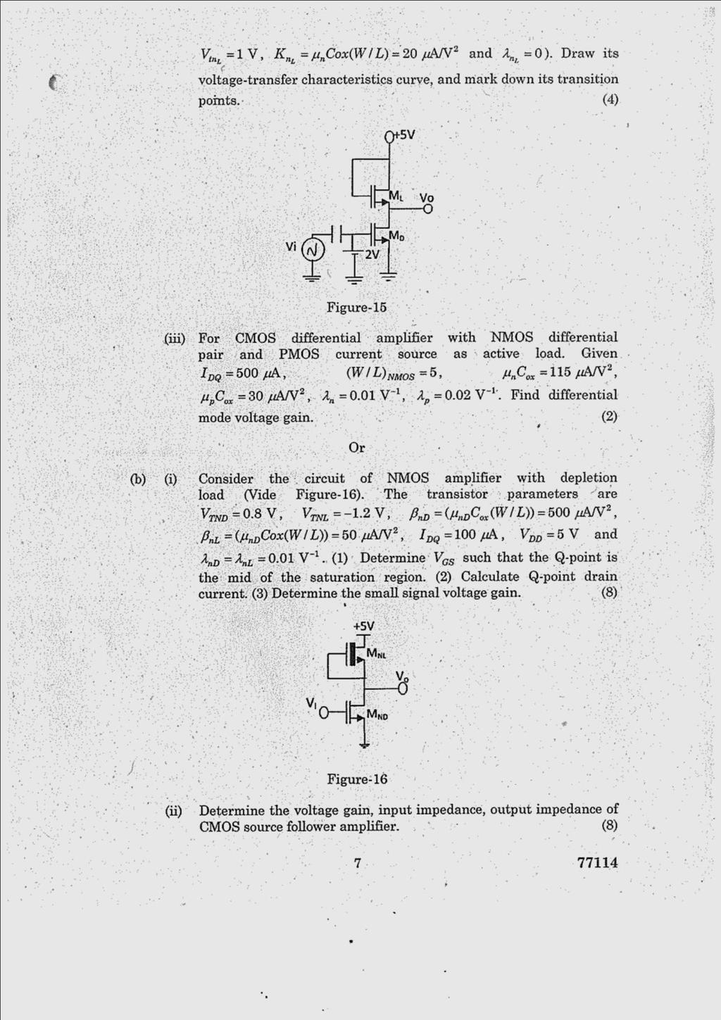
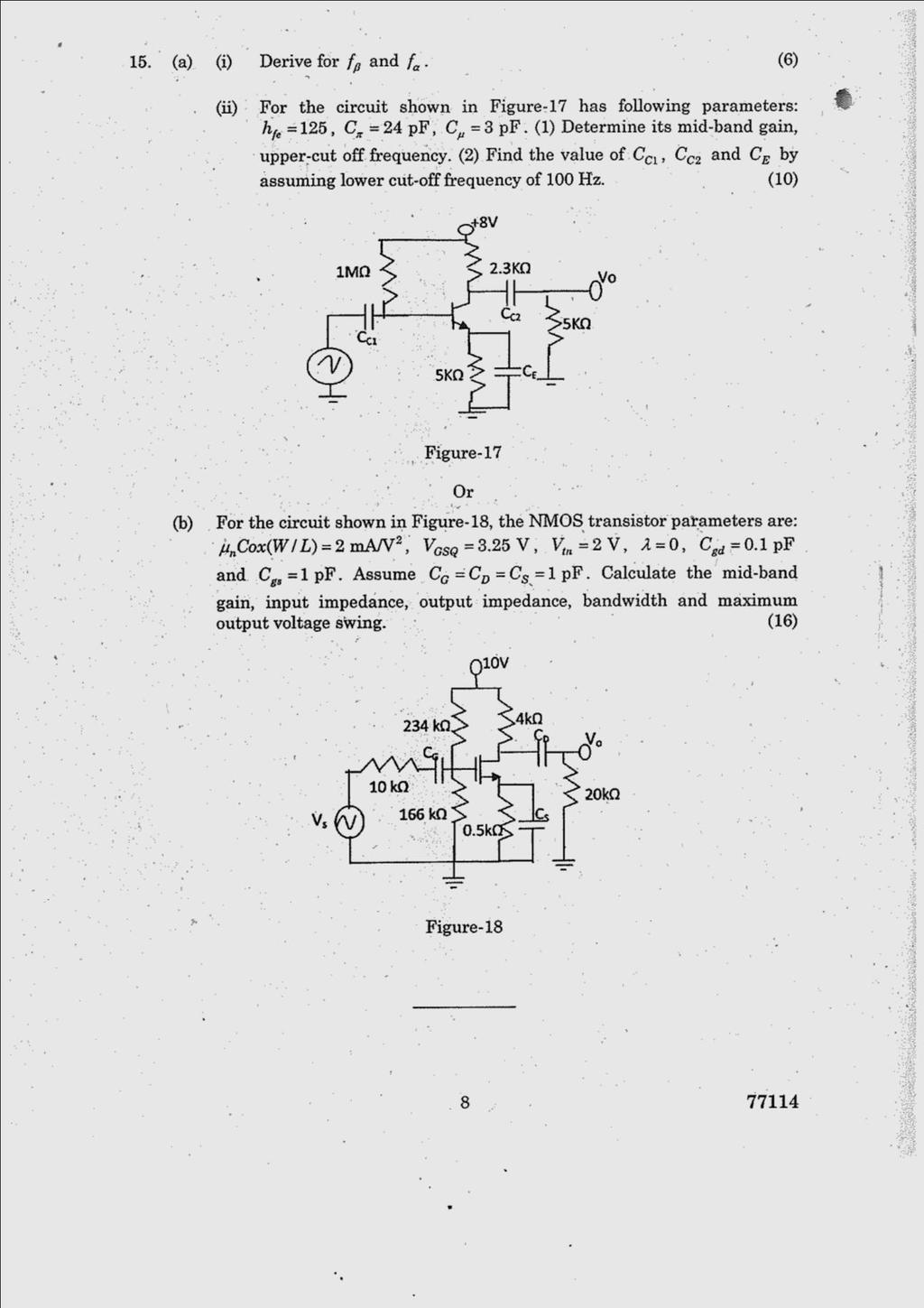
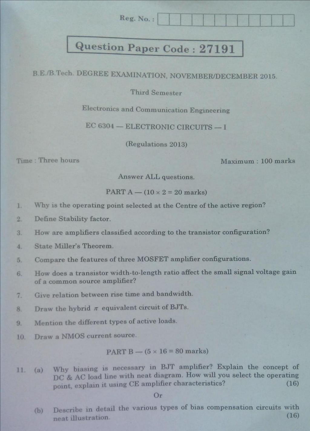
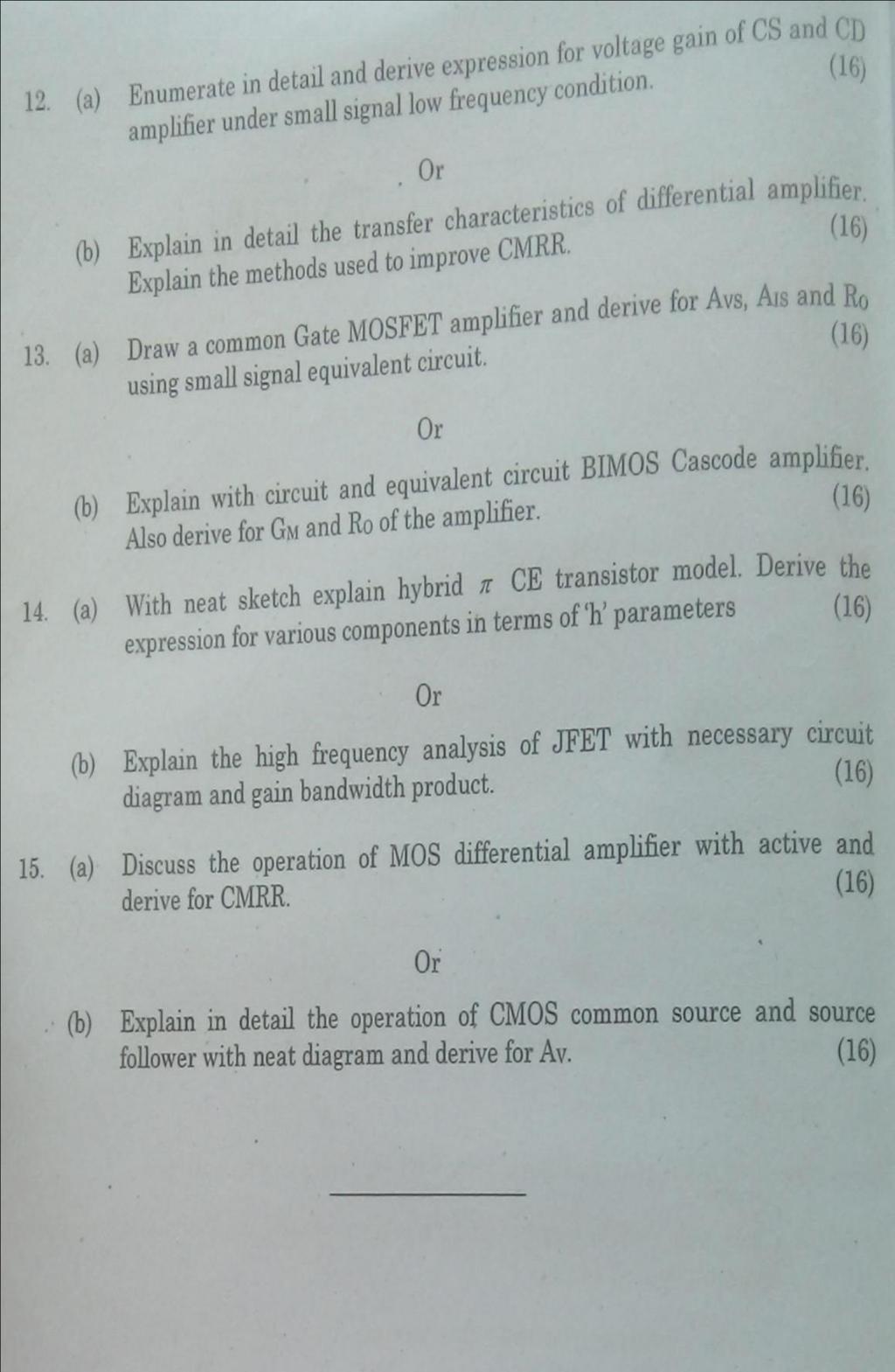
Vel Tech High Tech Dr.Ranagarajan Dr.Sakunthala Engineering College Department of ECE
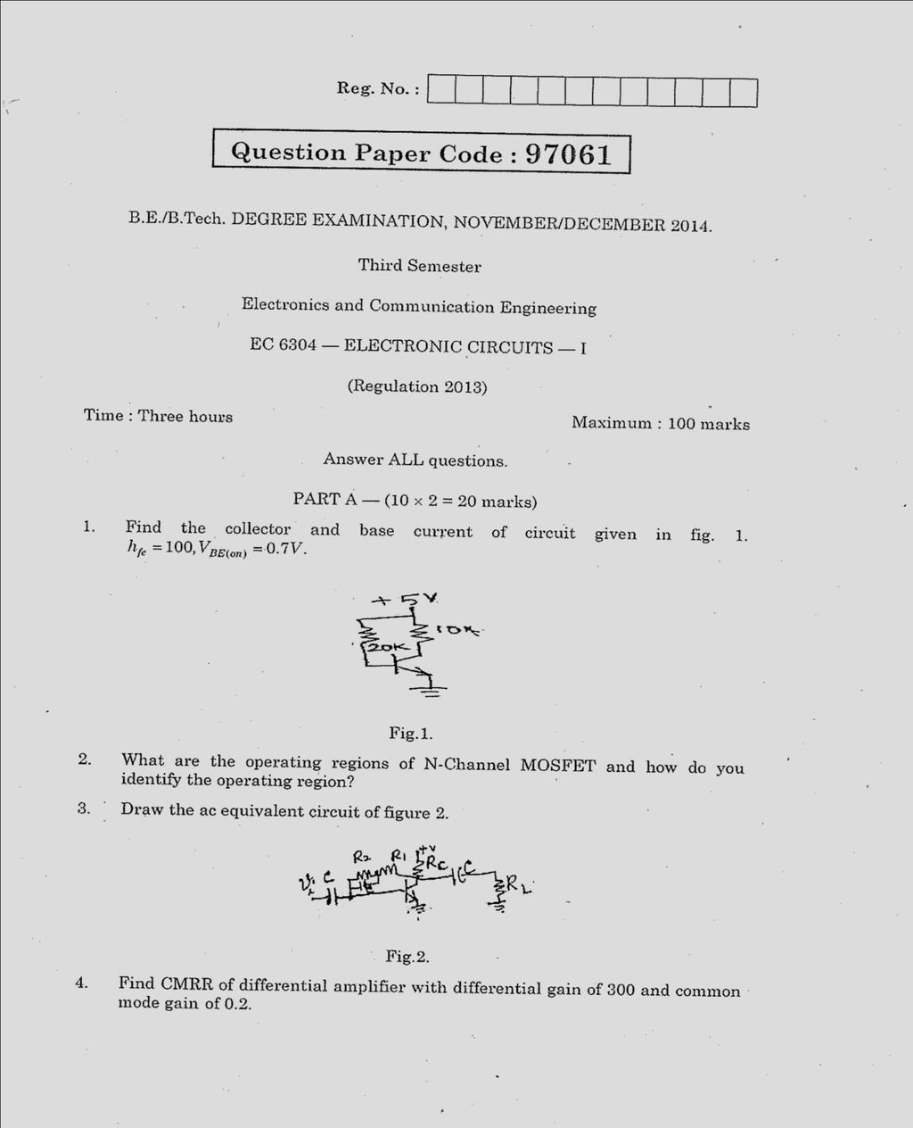
|
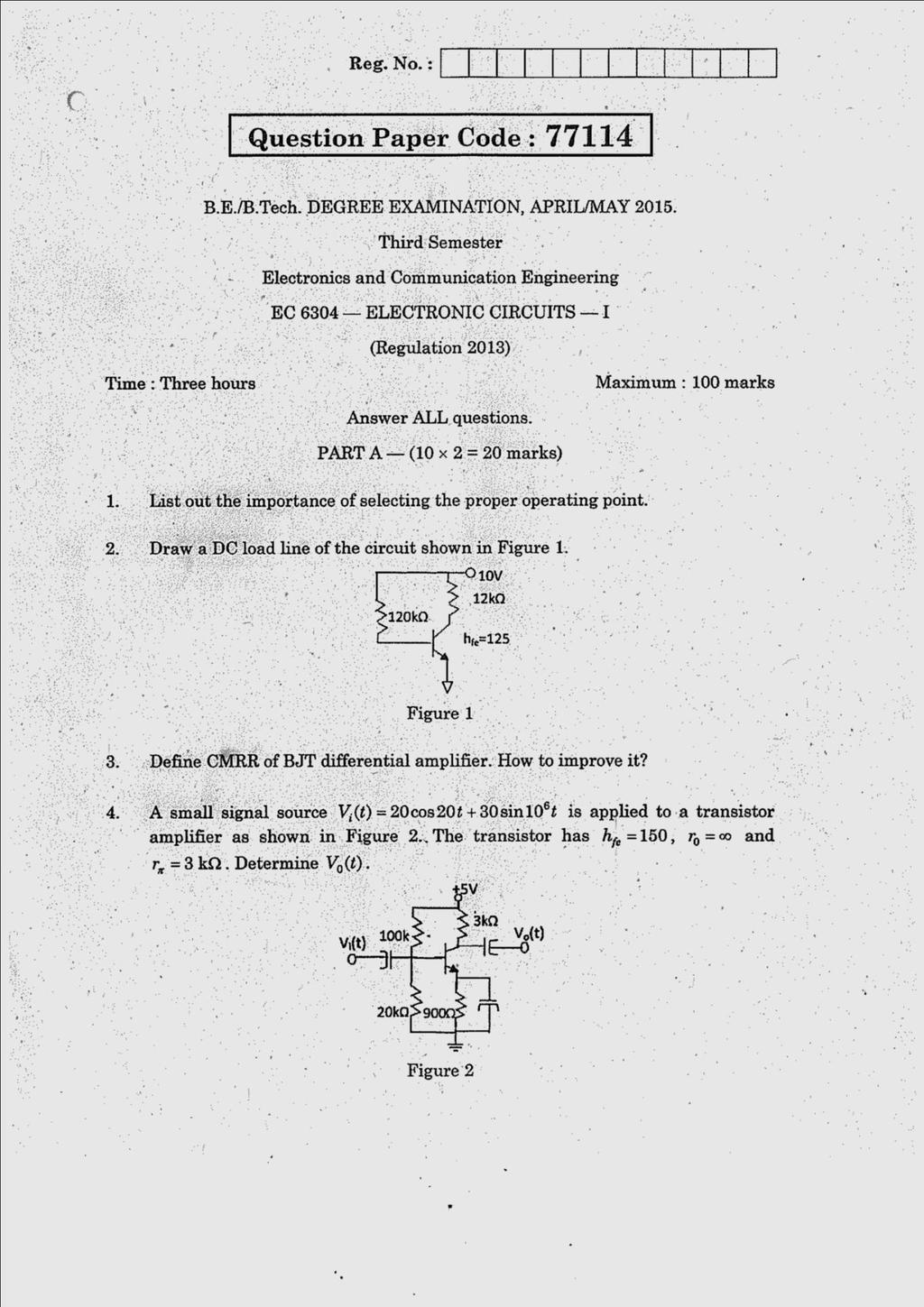
|
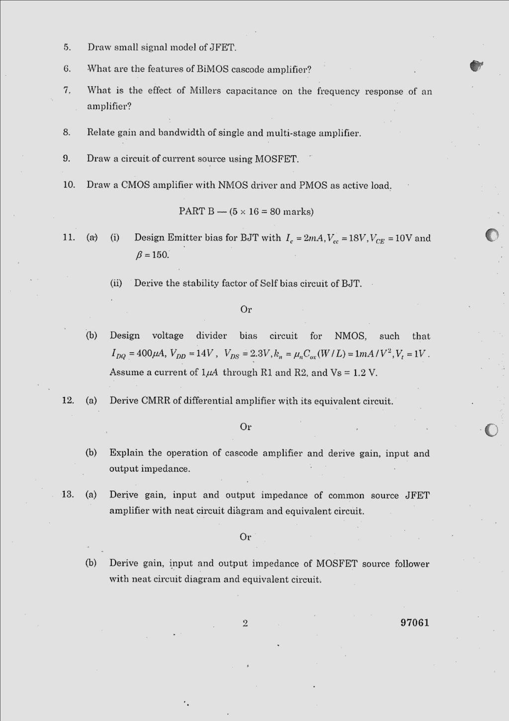
|
- Barbra Haynes
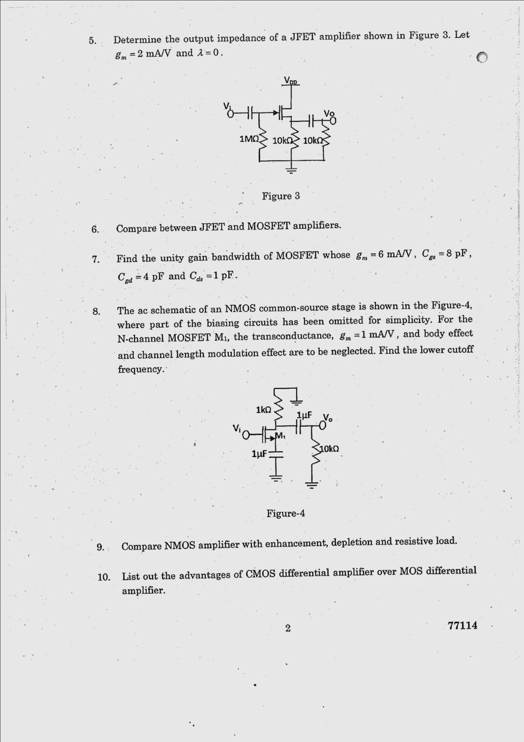
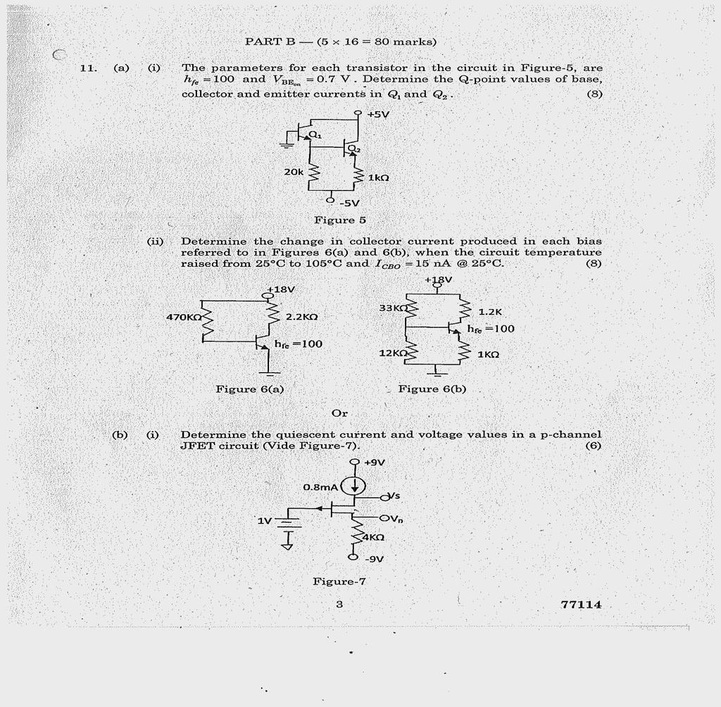
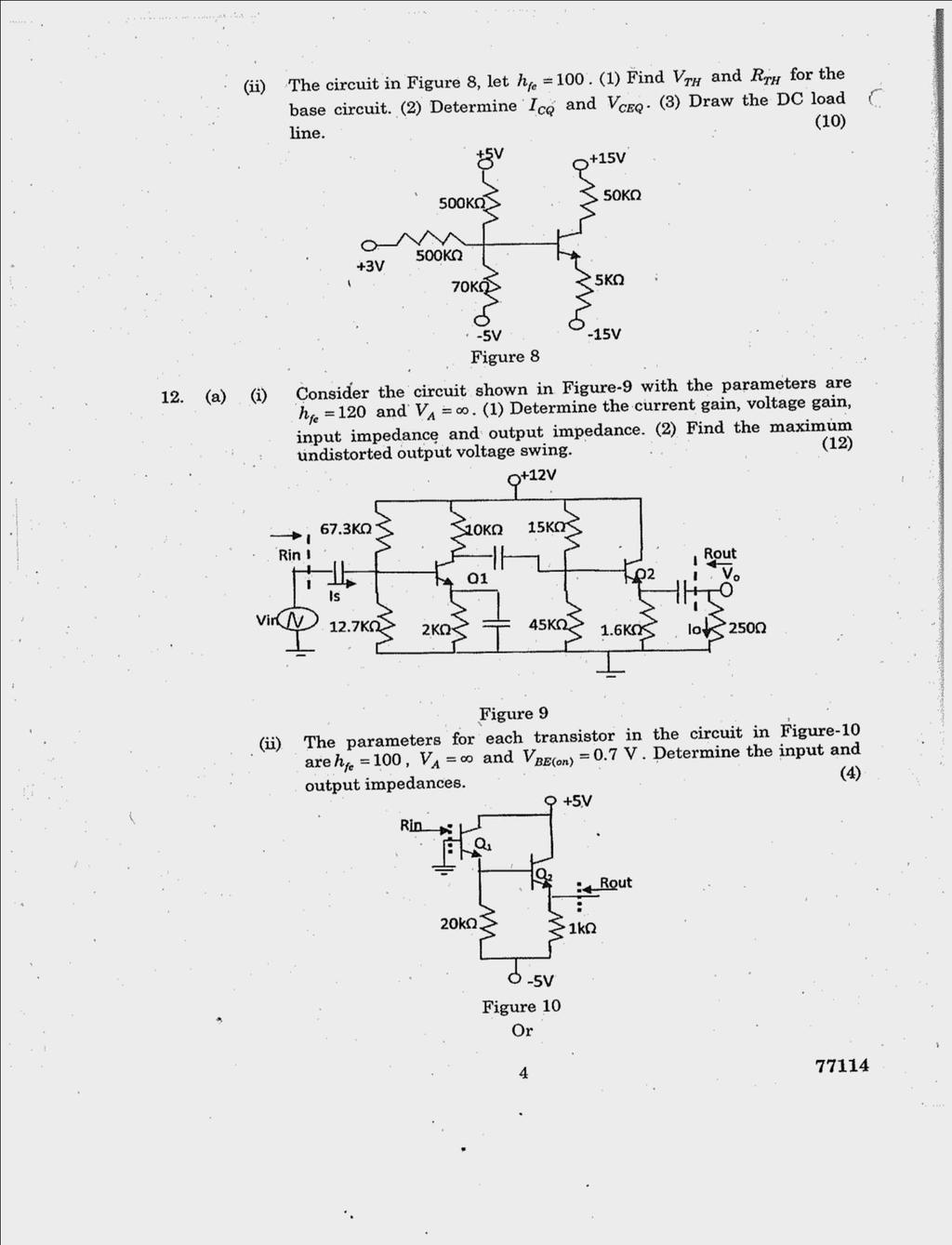
- 5 years ago
- Views:
Transcription
1 Course Code: EC8351 Course Name: ELECTRONIC CIRCUITS I L-3 : T-0 : P-0 : Credits - 3 COURSE OBJECTIVES: To understand the methods of biasing transistors To design and analyze single stage and multistage amplifier circuits To analyze the frequency response of small signal amplifiers To design and analyze the regulated DC power supplies. To troubleshoot and fault analysis of power supplies. COURSE OUTCOMES: At the end of the course, the student will be able to: CO No Course Outcomes Knowledge Level C203.1 Acquire knowledge of Working principles, characteristics and applications of BJT. K2 C203.2 Acquire knowledge of Working principles, characteristics and applications of FET. K2 C203.3 Frequency response characteristics of BJT and FET amplifiers K4 C203.4 Analyze the performance of small signal BJT and FET amplifiers - single stage and multi stage amplifiers K4 C203.5 Apply the knowledge gained in the design of Electronic circuits MAPPING OF COURSE OUTCOMES WITH PROGRAM OUTCOMES: K3 CO No. PO1 PO2 PO3 PO4 PO5 PO6 PO7 PO8 PO9 PO10 PO11 PO12 C C C C C CO No. PO1 PO2 PO3 PO4 PO5 PO6 PO7 PO8 PO9 PO10 PO11 PO12 C Mapping Relevancy 3 Substantial (Highly relevant) 2 Moderate (Medium) 1 Slight (Low) COURSE DELIVERY METHODS Class room lecture - Black board PPTs, Videos Lab Demonstrations Activities like In Plant Training, Live Demonstrations and Guest Lecture ASSESSMENT METHODS DIRECT ASSESSMENT Continuous Internal Assessment(CIA) End Semester Examination Assignments Seminars COURSE SYLLABUS Course Exit Survey Periodical Feedback INDIRECT ASSESSMENT UNIT I BIASING OF DISCRETE BJT, JFET AND MOSFET 9 BJT Need for biasing - DC Load Line and Bias Point DC analysis of Transistor circuits - Various biasing methods of BJT Bias Circuit Design - Thermal stability - Stability factors - Bias compensation techniques using Diode, thermistor and sensistor Biasing BJT Switching Circuits- JFET - DC Load Line and Bias Point - Various biasing methods of JFET - JFET Bias Circuit Design - MOSFET Biasing - Biasing FET Switching Circuits. UNIT II BJT AMPLIFIERS 9 Small Signal Hybrid π equivalent circuit of BJT Early effect - Analysis of CE, CC and CB amplifiers using Hybrid π equivalent circuits - AC Load Line Analysis- Darlington Amplifier - Bootstrap technique - Cascade, Cascode configurations - Differential amplifier, Basic BJT differential pair Small signal analysis and CMRR. UNIT III SINGLE STAGE FET, MOSFET AMPLIFIERS 9 Page 1
2 Amplifier frequency response Frequency response of transistor amplifiers with circuit capacitors BJT frequency response short circuit current gain - cut off frequency fα, fβ and unity gain bandwidth Miller effect - frequency response of FET - High frequency analysis of CE and MOSFET CS amplifier - Transistor Switching Times. UNIT IV FREQUENCY RESPONSE OF AMPLIFIERS 9 Amplifier frequency response Frequency response of transistor amplifiers with circuit capacitors BJT frequency response short circuit current gain - cut off frequency fα, fβ and unity gain bandwidth Miller effect - frequency response of FET - High frequency analysis of CE and MOSFET CS amplifier - Transistor Switching Times. UNIT V POWER SUPPLIES AND ELECTRONIC DEVICE TESTING 9 Linear mode power supply - Rectifiers - Filters - Half-Wave Rectifier Power Supply - Full- Wave Rectifier Power Supply - Voltage regulators: Voltage regulation - Linear series, shunt and switching Voltage Regulators - Over voltage protection - BJT and MOSFET Switched mode power supply (SMPS) - Power Supply Performance and Testing - Troubleshooting and Fault Analysis, Design of Regulated DC Power Supply. TEXT BOOKS: TB1. Donald. A. Neamen, Electronic Circuits Analysis and Design, 3rd Edition, Mc Graw Hill Education (India) Private Ltd., (Unit I-IV) TB2. Robert L. Boylestad and Louis Nasheresky, Electronic Devices and Circuit Theory, 11th Edition, Pearson Education, (Unit V) REFERENCES: RB1. Millman J, Halkias.C.and Sathyabrada Jit, Electronic Devices and Circuits, 4th Edition, Mc Graw Hill Education (India) Private Ltd., RB2. Salivahanan and N. Suresh Kumar, Electronic Devices and Circuits, 4th Edition,, Mc Graw Hill Education (India) Private Ltd., RB3. Floyd, Electronic Devices, Ninth Edition, Pearson Education, RB4. David A. Bell, Electronic Devices & Circuits, 5th Edition, Oxford University Press, RB5. Rashid M, Microelectronics Circuits, Thomson Learning, 2007 DEPARTMENT OF ECE COURSE DELIVERY PLAN COURSE INSTRUCTOR Dr.J.Veerappan FACULTY ID HTS1067 CURSE NAME ELECTRONIC CIRCUITS I COURSE CODE EC8351 YEAR/SEM II/III MONTH & YEAR JUNE S.No Date Unit Topic Text/ Reference Books Teaching Methodology Course Outcome I BJT Need for biasing C I DC Load Line and Bias Point Class room lecture - Black board C I DC analysis of Transistor circuits C203.1 Slip Test I Various biasing methods of BJT C I Bias Circuit Design -Thermal stability PPT Presentation C203.1 Stability factors - Bias compensation I RB1 C203.1 techniques I II II II Slip Test 2 I I Slip Test 3 II Slip Test 4 thermistor and sensistor Biasing BJT Switching Class room lecture - JFET - DC Load Line and Bias Point - Black board JFET C203.1 C203.1 MOSFET Biasing - Biasing FET Switching Circuits. PPT Presentation C203.1 Small Signal Hybrid π equivalent circuit of BJT Early effect - Analysis of CE, CC and CB amplifiers amplifiers using Hybrid π equivalent circuits AC Load Line Analysis- Darlington Amplifier - RB1 Class room lecture - Black board Class room lecture - Black board PPT C203.2 C203.2 C203.2 C203.2 Page 2
3 14 II Bootstrap technique Cascade configurations C II Cascode configurations C203.2 Slip Test 5 Differential amplifier, Basic BJT II Class room lecture - C203.2 differential pair Black board& Lab II Small signal analysis Demo C II CMRR CIA-1(UT-1&2) III Amplifier frequency response III Frequency response of transistor amplifiers PPT Presentation & Lab Demo Class room lecture - Black board C203.2 C203.3 C III BJT frequency response C203.3 Slip Test 6 short circuit current gain - cut off III C203.3 frequency fα, fβ Class room lecture III unity gain bandwidth Miller effect Black board C203.3 RB III frequency response of FET C III Slip Test 7 III High frequency analysis of CE amplifier MOSFET CS amplifier - Transistor Switching PPT & Videos C203.3 C III Transistor Switching Times. C203.3 Slip Test IV Amplifier frequency response C short circuit current gain - cut off 31 IV C203.4 frequency fα, fβ RB2 Class room lecture IV unity gain bandwidth Miller effect Black board C203.4 IV IV CIA-2(UT-1,2&3) Frequency response of transistor amplifiers with circuit capacitors BJT frequency response Class room lecture - Black board C203.4 C IV High frequency analysis of CE C IV Slip Test 9 High frequency analysis of MOSFET CS amplifier - Class room lecture - Black board C IV Transistor Switching PPT & Videos C IV V V V V Slip Test 10 Slip Test 11 Transistor Switching Times. Linear mode power supply - Rectifiers - Filters - Half-Wave Rectifier Power Supply - FullWave Rectifier Power Supply - Voltage regulator Voltage regulation - Linear series, shunt RB2 Class room lecture - Black board PPT & Videos Class room lecture - Black board C203.4 C203.5 C203.5 C203.5 C203.5 Page 3
4 V switching Voltage Regulators C V Over voltage protection - BJT and MOSFET C203.5 Slip Test V Switched mode power supply (SMPS C V V Power Supply Performance and Testing Troubleshooting, Design Regulated Power Supply. Class room lecture - Black board C203.5 C203.5 CIA-3(UT-4&5) CIA-4(ALL 5 UNITS) CO 1,2,3,4,5 UNIT -1 BIASING OF DISCRETE BJT AND MOSFET 1) Why do we choose Q point at the center of the load line. (NOV 2016) (APR 2015) (NOV 2015) The operating point of a transistor is kept fixed usually at the center of the active region in order that the input signal is well amplified. If the point is fixed in the saturation region or the cut off region the positive and negative half cycle gets clipped off respectively. 2) Name the two techniques used in the stability of the Q point. Stabilization technique: This refers to the use of resistive biasing circuit which allows IB to vary so as to keep IC relatively constant with variations in Ico,_, and VBE. Compensation techniques: This refers to the use of temperature sensitive devices such as thermistors diodes. They provide compensating voltages ¤ts to maintain operating point constant. 3) Give the expression for the stability factor 4) List out the difference types of biasing. Voltage divider bias Base bias Emitter feed back bias Collector feedback bias 5) What do you mean by thermal runway? Due to the self heating at the collector junction, the collector current rises. This causes damage to the device. This phenomenon is called thermal runway. 6) What is Biasing To use the transistor in any application it is necessary to provide sufficient voltage and current to operate the transistor. This is called biasing. 7) What is stability factor? (NOV 2015) Stability factor is defined as the rate of change of collector current with respect to the rate of change of reverse saturation current. 8) What are the advantages of fixed bias circuit. This is simple circuit which uses a few components. The operating point can be fixed any where on the Centre of the active region 9) List the advantage of Transistor? Low operating voltage High Frequency Page 4
 Define DC Biasing In order to operate transistor in the desired region we have to apply external DC voltage of correct polarity and magnitude to the two junctions of the transistor.")
5 Small Size and ruggedness Does not require filament power. 10 ) Define DC Biasing In order to operate transistor in the desired region we have to apply external DC voltage of correct polarity and magnitude to the two junctions of the transistor. 11 what are the factors against which an amplifier need to be stabilized? The stability factor indicates the degree of charge in operating point due to variation in β,ic 0 and V BE 12) Define Stability Factor. (APR 2017) Stability factor is defined as the rate of change of collector current with respect to the rate of change of reverse saturation current. 13) Why thermal runaway is not there in FETs? FET is temperature dependent. In FET, as temperature increases drain resistance also increases, reducing the drain current. So thermal runaway does not occur in FET. 14) What is meant by compensating techniques? (MAY/JUNE-2006) Use of temperature-sensitive devices such as diodes, transistors, thermistors, etc., which provide compensating voltages and currents to maintain the operating point stable. 15) Write short notes on zero current drift in FET (APRIL/MAY-2008) In JFET, the drain current varies with changes in the temperature due to two factors. One factor increases drain current and other factor decreases drain current with increase in temperature. Therefore, it is possible to design biasing circuit which compensates these tow factors so that there is no c hange of drain current with temperature. Such biasing is called biasing for zero current drift. 16) Draw the fixed bias & Self bias circuit? 17) For the circuit shown in figure determine the operating point with B= ) What is reverse saturation current? The current due to the minority carriers is called the reverse saturation current. Page 5
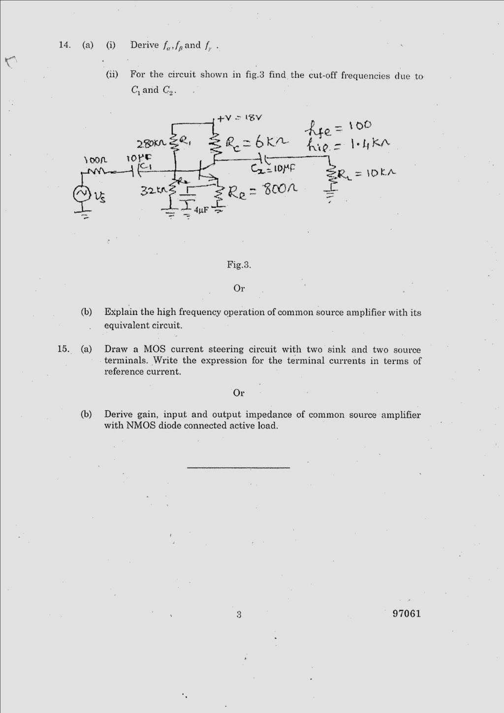
6 19) How are amplifier classified according to the input? Small signal Amplifiers Large signal Amplifiers 20) What is operating point. The operating point of a device, also known as bias point, quiescent point, or Q-point, is the steady-state voltage or current at a specified terminal of an active device (a transistor or vacuum tube) with no input signal applied. Part B (16 Marks) 1) Explain the voltage divider bias method & derive an expression for stability factors. 2. Why biasing is necessary in BJT amplifier? Explain the concept of DC & AC load line with neat diagram. How will you select the operating point, explain it using CE amplifier characteristics? 3. Explain the collector feedback bias amplifier & derive an expression for stability factors. 4. Explain the fixed bias method & derive an expression for stability factors. 5. Derive an expression for all stability factors & CE configuration S equation. 6. Explain about common source self- bias & voltage divider bias for FET. 7. Explain in details about biasing MOSFET. 8. Discuss the various types of bias compensation. 9. The fixed bias circuit as shown in figure is subjected to an increase in junction temperature from 25oC to 75oC. If β is 125 at 75oC. Determine the percentage change in Q point values (Vce, Ic) over temperature change. Neglect any change in VBE. 10. A self bias circuit has RE=1 kω, R1=130 kω, R2=10 kω. If Vcc and Rc are adjusted to give Ic=1mA at 10oC. Calculate the variation in Ic over temperature change of 10oC to 100oC. The transistor used has the parameters given below Parameters o 100 o C Ico (µa) C VBE(v) β Page 6
7 11. Design a collector to base bias circuit to have operating point (10v, 4mA). The circuit is supplied with 20v and uses a silicon transistor of hfe is Design a voltage divider bias circuit for the specified conditions. VCC=12v, VCE=6v, IC=1mA, S=20, β=100 and VE=1v UNIT -2 BJT AMPLIFIERS 1) What is the overall current gain for a cascade connection? The overall current gain of cascade connection is 2 ) What does Bootstrapping Mean? When AV=1 it is called bootstrapping. The name arises from the fact that, if one end of the resistor R3 changes in voltage, the other end of R3 moves through the same potential difference; it is as if R3 is pulling itself up by its bootstraps. 3) State Miller s Theorem.(NOV/DEC-2006),(APRIL/MAY-2008) (APR 2017) (NOV 2015) Miller s theorem states that, the effect of resistance Z on the input circuit is a ratio of input voltage Vi to the current I which flows from the input to the output. Miller s theorem states that, the effect of resistance Z on the output circuit is a ratio of output voltage Vo to the current I which flows from the output to the input. 4) What are the techniques used to improve input impedance. 5) Give the advantages of h- parameters. Real numbers at audio frequencies Easy to measure Can be obtained from the transistor static characteristic curves Convenient to use in circuit analysis and design. Page 7
8 Most of the transistor manufacturers specify the h-parameter. 6) Define CMRR? (NOV 2016) (APR 2015) The ability of a differential amplifier to reject a common mode signal is expressed by a ratio called common mode rejection ratio denoted as CMRR. It is defined as the ratio of the differential voltage gain Ad to common mode voltage gain Ac CMRR= (Ad / Ac) 7) State the equation of Ad & Ac. Ad(db) = 20 log 10 [vo/vd] 8) How CMRR can be improved. To improve the CMRR, the common mode gain Ac must be reduced. The common mode gain Ac approaches zero as RE tends to infinity. This is because RE introduces a negative feedback in the common mode operation which reduces the common mode gain Ac. Thus higher the value of RE, lesser is the value of Ac and higher is the value of CMRR. The differential gain Ad is not dependent on RE. 9) State the methods of coupling multistage amplifiers. (NOV 2016) RC coupling Transformer coupling Direct coupling 10) State the advantages of RC Coupled Amplifier. Wide frequency response Most convenient coupling No core distortion High fidelity Amplifier 11)State the application of Transformer Coupled Amplifier. For Impedance Matching For amplification of RF Signal In Power Amplifiers Transforming power to low impedance load 12) Draw the Darling ton pair connection diagram? 13) State the advantages of Darlington emitter follower. Page 8
 What do you mean by faithful amplification?")
9 14) State the features of Darlington emitter follower. Very high current gain Very low voltage gain Very high input resistance Very low output resistance 15) What do you mean by faithful amplification? The shape of the output voltage is exactly same as that of input. That means no waveform distortion has taken place. The process of raising the strength of a weak signal without any change in its general shape is known as faithful amplification. 16) State the various two stages cascaded amplifiers. CE-CE CASCADE CC-CE CASCADE CE-CC CASCADE CE-CB CASCADE CB-CC CASCADE CC-CB CASCADE 17. Define class C operation of power amplifier? In a class C amplifier the transistor bias and amplitude of the input signal are selected such that the output current flows the transistor is ON for less than one half cycle of the input ac signal. 18. Why class A amplifier must not be operated under no signal conditions? When there is no input signal the power dissipation must be zero, but here the power dissipation is present due to this reason the class A power amplifier is not used under any signal condition. 19.Which power amplifier gives minimum distortion and Why? Class A Power amplifier is distortion free Collector current flows for the whole that is for 360 degree of the input cycle. 20. When does inter modulation distortion occur? Why should it be minimized in audio amplifier? Inter modulation distortion an amplifier arises when the input signal consists of two different frequencies f1 and f2. If the active device is nonlinear the output consists of fundamental the harmonic components f1+f2 and f1-f2. These frequencies are called inter modulation distortion. It may not to be eliminated. 21. What is the drawback of class B amplifier? How is this minimized? In class B amplifier only a half cycle is obtained at the output for full input cycle the output signal is distorted in this mode of operation. to eliminate this distortion two transistor are used in the alternate half cycle of the input signal. Thus the overall full cycle of output is obtained across the load because each transistor conducts for half cycle. 22. What are the advantages of push pull amplifier? Page 9
10 Efficiency is much higher than the class A operation When there is no input signal the power dissipation is zero The even harmonics get cancelled. this reduces the harmonic distortion 23. What is cross over distortion? How it can be eliminated. In class B amplifier the transistor is supposed to operate for full half cycle of the input. But Because of the cut in voltage, the transistor starts conducting only after 0.7V. the distortion caused by this is called cross over distortion. This can be eliminated by using two complementary transistor to conduct in alternate half cycle. PART B ( 16 MARKS) 1) Draw a CE amplifier & its small signal equivalent. Derive its Avs, Ai, Rin, Ro. 2. Explain with circuit diagram of Darlington connection and derive the expression for Ai, Av, Ri &Ro. 3. Explain Bootstrap emitter follower circuit. Compare CE, CB, CC amplifiers. 4. Derive expression for voltage gain of CS & CD amplifier under small signal low frequency condition. 5. Explain the emitter coupled differential amplifier with neat diagram & Derive expression for CMRR. 6. Discuss transfer characteristics of differential amplifier. Explain the methods used to improve CMRR. 7. Write short notes on multistage amplifiers & Draw a two stage RC coupled amplifier and explain. Compare cascade and cascode amplifier? 8. Derive the expressions for the voltage gain, current gain, input and output impedance of emitter follower amplifier. 9. Derive the expressions for the common mode and differential mode gains of a differentia amplifier in terms of h-parameters. 10. Consider a single stage CE amplifier with Rs=1kΩ, R1=50KΩ, R2=2KΩ, RC=2KΩ, RL=2KΩ, hfe=50, hie=1.1 KΩ, hoe=25µmho, hre= Find Ai,Ri,Av,Ais,Avs and R The Darlington amplifier has the following parameters, Rs=3kΩ, RE=3kΩ, hie=1.1 KΩ, hfe=50, hre= , hoe=25µmho. Then calculate Ai, Ri, Av and R0. Page 10
11 12. The dual input balanced output differential amplifier having Rs=100Ω, RC=4.7KΩ, RE=6.8KΩ, hfe=100, Vcc=+15v and VEE=-15v. Calculate operating point values, differential & common mode gain, CMRR, and output if VS1= 70mV(p-p) at 1 KHz & VS2= 40mV(p-p) at 1 KHz 13 Explain in detail class A power amplifier with a neat sketch 14 Explain in detail class B & C power amplifier with a neat sketch 1) List the different types of FET biasing circuits. Fixed Bias Self Bias Voltage Divider Bias UNIT III JFET AND MOSFET AMPLIFIERS 2) State the general procedure for analysis of a JFET biasing Circuit. Calculate VGs by applying KVL to the gate circuit Calculate IDg by using Shockleys equations Calculate VDSq by applying KVL to the drawn loop 3) Draw the source self bias circuit for FET. 4) Draw the voltage divider bias circuit for FET. Page 11
12 5) State the basic configuration of an E-MOSFET. Common source Common gate Common drain 6) Why thermal runaway is not there in FETs? Thermal runaway is not there in FET because the FET has a positive temperature coefficient of resistivity it means increase in temperature the resistance of an FET increases and hence the current through it decreases so the power dissipation decreases so it prevents thermal runaway. 7) Explain the use of JFET as a variable voltage resistor. The FET can be used as variable voltage resistor in the region called ohmic. Since the drain to source resistance VDs in this region dependent on the gate to source voltage. 8) Draw the small signal equivalent circuit of FET. (NOV 2014) 9) State the application of CS Amplifier. Pre Amplifier in audio circuits P.A System Voltage Amplifier 10) Draw the diagram of JFET Common Drain Configuration. 11) State the features of Common Drain Amplifier. Low voltage gain Very high input resistance Very low output resistance 12) State the procedure to be followed for the small signal analysis. Replace all the capacitors in the given circuit by short circuits. Replace all the DC voltage source by short circuit Replace the JFET in the circuit by its AC equivalent Calculate the Amplifier Parameters Page 12
13 13) State the formula to calculate transconductance. 14) Draw the circuit diagram of CSJFET Amplifier with self Bias. 15) Draw the source follower configuration circuit. 16) Two amplifiers having gain 20db & 40db are cascaded find the overall gain in db. Overall gain = = 60 Db 17) Draw the small signal equivalent of NMOS cascade circuit Page 13
14 18) Draw the circuit diagram of multistage Amplifier cascade common. 19) Draw the voltage divider bias circuit. 20) Draw the diagram of AGC Amplifier. 21) What is the use of bypass source capacitor in CS amplifier? (APR 2017) For improving the voltage gain PART B 16 MARKS 1. Describe the operation and analyze the basic JFET amplifier circuits. 2. Derive the small signal analysis of common source amplifier. Page 14
15 3. Develop a small signal model of JFET device and analyze basic JFET amplifiers. 4. Explain graphically the amplification process in a simple MOSFET amplifier circuit. 5. Describe the small signal equivalent circuit of the MOSFET and determine the values of small signal parameters? 6. Sketch the small signal high frequency circuit of a common source amplifier & derive the expression for a voltage gain, input & output admittance and input capacitance. 7. Sketch a simple source-follower amplifier circuit and discuss the general ac circuit characteristics. 8. Characterize the voltage gain and output resistance of a common-gate amplifier. 9.Calculate the small signal voltage gain of a common source amplifier such as shown in the figure assuming gm=1ma/v, ro=50 K and Rd=10 K, Assume RSi = 2k & R1parallel R2=50K. 10.The parameters of the MOSFET in the Circuit are VTN=0.8 V,Kn=0.85mA/V2 & λ=0.02 V Determine the values of Rs & Rd such that IDq=0.1ma and a maximum symmetrical 1 V peak sinusoidal signal occurs at the output find the small signal transistor parameters 11.Explain in detail BIMOS Cascade Amplifier. 12.Compare CS,CD,CG Configuration. 13.With the help of neat circuit diagram and waveform explain the operation of a CD or Souce amplifier of JFET UNIT IV FREQUENCY ANALYSIS OF BJT & MOSFET AMPLIFIER 1)What is bandwidth of an amplifier? Band width of an amplifier is defined as the difference between f1 and f2. Here f2 is in the high frequency region and f1 is in the low frequency region. These two frequencies are also referred to as the half power frequencies. 2) How the rise time and bandwidth are interrelated?(apr 2017) (NOV 2014) (NOV 2015) Bw = FH FL~ FH BW = 0.35/ tr 3) How the frequency response of an amplifier be improved? The frequency response can be improved by connecting the compensating network externally to the system. Such Techniques are as follows i) Dominant pole Compensation ii) Pole zero Compensation Page 15
16 4) Define the rise time of an amplifier. It is defined as the time that indicates how fast the amplifiers can response to the discontinuity in the input voltage. 5 ) Define Slew Rate? Slew rate can be defined as the maximum rate of change of output voltage of op-amp with respect to time. 6) What are high frequency effects. When the frequency is increased sufficiently the internal capacitances which affects the voltage gain. In high frequency range the coupling and bypass capacitor offer a very low reactance and they can be treated as short wave. 7 ) Define duty cycle in an amplifier. Duty cycle is the fraction of one complete cycle for which the amplifier is in active region operation. 8) What are the effects of coupling capacitors on the bandwidth of the amplifier? The capacitor C! & C2 are coupling capacitors used for blocking the DC part and allowing only AC part of the signal. The capacitive reactance will increase with decrease in frequency and it will decrease with increase in frequency. 9) Define Dominant network. The RC network having the highest critical frequency of the three networks is refered to as dominant network. 11) State the relation Fβ & Fα. Fα=(1+hfe)Fβ 12) Briefly explain why dominant pole high frequency compensation method used in amplifiers. As the noise frequency components are outside the smaller bandwidth, The noise immunity of the system improves. Adjusting value of fd adequate phase margin and stability of the system is assured. 13) C a l c u l a t e t h e ov e r a l l l o w e r c u t o f f fre q u e n c y. ( NOV 2016) 14 D r a w t h e c i r c u i t of R C C o u p l e d J F E T A m p li f i e r. 15) Define sag in an amplifier The lower 3 db frequency can be eliminated from the output by measuring the sag 16.State the expression for unity gain frequency. Page 16
17 17.State the effect of bypass capacitor in FET Amplifier. The bypass capacitor is present in FET amplifier as it bypasses the resistance connected in the source terminal of the FET. 18.Define the benefits of H-parameters. Real numbers at audio frequencies Easy to measure Can be obtained from the transistor static characteristic curves Convenient to use in circuit analysis and design. Most of the transistor manufacturers specify the h-parameter. 19. Define Decibel. To compare two power on a log scale rather than on a linear scale. It is known as decibel (db) 20. Write short note on gain bandwidth product. The gain bandwidth product is Gain X BW + Constant 21 Relation between bandwidth and rise time. (APR 2017) The rise time is the time required for a signal to change from 10% value to a 90% of its value. Bandwidth=0.35/t r Part B (16 Marks) 1. With neat sketch explain hybrid π CE transistor model. Derive the expression for various components in terms of h parameters. 2. Discuss the frequency response of multistage amplifiers. Calculate the overall upper & lower cutoff frequencies. 3. Discuss the low frequency response & the high frequency response of an amplifier. Derive its cutoff frequencies. 4. Discuss the terms rise time and sag. 5. Write short notes on high frequency amplifier. 6. Derive the gain bandwidth for high frequency FET amplifiers. 7. Derive the expression for the CE short circuit current gain of transistor at high frequency. 8. What is the effect of Cb e on the input circuit of a BJT amplifier at High frequencies? Derive the equation for gm which gives the relation between gm, Ic and temperature. 9. Explain the high frequency analysis of JFET with necessary circuit diagram & gain bandwidth product. Page 17
18 10. Discuss the frequency response of MOSFET CS amplifier. 11. Determine the bandwidth of CE amplifier with the following specifications. R1=100kΩ, R2=10kΩ, RC=9kΩ, RE=2kΩ, C1= C2=25µF, CE=50µF, rbb =100Ω, rb e=1.1kω, hfe=225,cb e=3pf and Cb c=100pf. 12. At Ic=1mA & VCE=10v, a certain transistor data shows Cc=Cb c=3pf, hfe=200, & ωt=-500m rad/sec. Calculate gm, rb e, Ce=Cb e & ωβ. 13. Derive the expression of Fβ & Fα 14. Derive the expression for CE short circuit gain using Hybrid π model 15. Explain the briefly the various stages of Multistage amplifiers 16. for the FET Amplifier the component value are Rd =2.2 K, Rl =4.7K Rg=10M,Rs=600cgd=2PF cgs=4pf gm=4ms. Determine high frequency of amplifier UNIT V MOSFET AMPLIFIER 1) Draw the circuit for a basic MOSFET constant circuit source. (NOV 2014) (NOV 2015) 2) State the basic gain cell in Ic. 3) Draw the small signal analysis circuit for determine voltage gain & Av. 4) Draw the circuit design of PMOSFET CS Amplifier. Page 18
19 5 ) Why do we amplify a signal? The signal is to small to due to load to overcome the noise of a subsequent stage we need to amplify the signal in order to obtain high f=gain factor 6) Draw the source follower amplifier circuit 7) State the advantages of differential pair. Less sensitive to noise Bias is provided without need for by pass 8) Define current steering. (APR 2017) On an Ic Chip with a number of amplifier stages, a constant dc current is generated at one location and then replicated at various other locations for biasing the various amplifiers stages through a process known as current steering. 9) Draw the general MOS differential Amplifier 10) Draw the small signal mode of Differential amplifier. 11) What is the need of constant current in differential amplifier. The necessary for constant current source for differential amplifier to increase the CMRR without changing quiescent current and without lowering the forward current gain. 12) List the application of MOSFET power amplifier.. It is used in amplification process 13) What is distortion in power Amplifier? Page 19
20 In an ideal amplifier all frequency components of the signal amplifies proportionally hence the output signal is the exact repetition of the input signal. 14) Define active load and list the types of active load. (APR 2017) (NOV 2014) (APR 2015) (NOV 2015) The MOS transistor used as a load device is referred to as active load. Three types of load devices are n- channel enhancement load device, n channel depletion load device and p channel enhancement load device. 15) State the advantages of current steering. (APR 2017) Effort expended on generating a predictable and stable reference current usually utilizing a precision resistor external to the chip need not be repeated for every amplifier stage. The bias currents of the various stages track each other in case of changes in power supply voltage or in temperature. 16) Draw the basic MOSFET constant current source. 17) Define voltage gain. The ratio of output voltage to input voltage is called voltage gain Av of the amplifier Av=V2/V1 18) List the features of Differential Amplifiers. High differential voltage gain Low common mode gain High CMRR Two input terminals High input impedance Large bandwidth 19) What are the other methods to improve CMRR without RE? (APR 2015) Constant current bias method Current mirror method 20 ) List the application of Differential Amplifier. Limiter Amplitude Modulation PART B ( 16 MARKS) Page 20
21 1. Describe the operation of an NMOS amplifier with either an enhancement load, a depletion load, or a PMOS load. 2. Explain the basic MOSFET two transistor current circuits and discuss its operation. 3. Draw the MOSFET Cascode current source circuit, explain and discuss the advantage of this design. 4. Sketch and describe the advantages of a MOSFET Cascode current source used with a MOSFET differential amplifier. 5. Design a CMOS differential amplifier with an output gain stage to meet a set of specifications. The magnitude of voltage gain of each stage is to be at least 600. Bias currents are to be IQ=IREF=100µA, and biasing of the circuit is to be V+=2.5 v and V-=2.5 v. 6. Explain CMOS differential amplifier and derive CMRR. 7. Draw a Widlar current source and explain the operation. 8. Describe the operation of a PMOS amplifier with an enhancement load, a depletion load. 9. Explain the CMOS common source and source follower with neat diagram. 10.Explain the various current steering circuit used in MOSFET 11. Explain and derive the expression of Current of PMOS 12.Explain with a neat diagram PMOS Current Source 13. Derive the parameter of NMOS Amplifier with active load in Enhancement mode 14. Derive the parameters of PMOS amplifier in depletion mode 15. Compare IC Biasing current steering circuit with differential amplifier 16. Calculate the coupling capacitor Cc required to provide a low frequency 3db p out at 125 H if Rs = 600,Fie=1K,hfe=60,R1=5K,R2=1.25K. For an ideal by pass capacitor a practical by pass capacitor Rce+25 Page 21
22 Page 22
23 Page 23
24 Page 24
25 Page 25
26 Page 26
27 Page 27
28 Page 28
29 Page 29
30 Page 30
31 Page 31
32 Page 32
33 Page 33
34 Page 34
35 Page 35
36 Page 36
37 Page 37
38 Page 38
39 Page 39
40 Page 40
41 Page 41
42 Page 42
UNIT I BIASING OF DISCRETE BJT AND MOSFET PART A
 UNIT I BIASING OF DISCRETE BJT AND MOSFET PART A 1. Why do we choose Q point at the center of the load line? 2. Name the two techniques used in the stability of the q point.explain. 3. Give the expression
DEPARTMENT OF ELECTRONICS AND COMMUNICATION ENGINEERING III SEMESTER EC 6304 ELECTRONIC CIRCUITS I. (Regulations 2013)
") DEPARTMENT OF ELECTRONICS AND COMMUNICATION ENGINEERING III SEMESTER EC 6304 ELECTRONIC CIRCUITS I (Regulations 2013 UNIT-1 Part A 1. What is a Q-point? [N/D 16] The operating point also known as quiescent
DEPARTMENT OF ELECTRONICS AND COMMUNICATION ENGINEERING III SEMESTER EC 6304 ELECTRONIC CIRCUITS I (Regulations 2013 UNIT-1 Part A 1. What is a Q-point? [N/D 16] The operating point also known as quiescent
 Pg: 1 VALLIAMMAI ENGINEERING COLLEGE SRM Nagar, Kattankulathur 603 203 Department of Electronics & Communication Engineering Regulation: 2013 Acadamic Year : 2015 2016 EC6304 Electronic Circuits I Question
Unit- I- Biasing Of Discrete BJT and MOSFET
 Part- A QUESTIONS: Unit- I- Biasing Of Discrete BJT and MOSFET 1. Describe about BJT? BJT consists of 2 PN junctions. It has three terminals: emitter, base and collector. Transistor can be operated in
SKP Engineering College
 SKP Engineering College Tiruvannamalai 606611 A Course Material on Electronic Circuits I By M.Jerin Jose Assistant Professor Electronics and Communication Engineering Department Electronics and Communication
BJT Circuits (MCQs of Moderate Complexity)
") BJT Circuits (MCQs of Moderate Complexity) 1. The current ib through base of a silicon npn transistor is 1+0.1 cos (1000πt) ma. At 300K, the rπ in the small signal model of the transistor is i b B C r
BJT Circuits (MCQs of Moderate Complexity) 1. The current ib through base of a silicon npn transistor is 1+0.1 cos (1000πt) ma. At 300K, the rπ in the small signal model of the transistor is i b B C r
EC1203: ELECTRONICS CIRCUITS-I UNIT-I TRANSISTOR BIASING PART-A
 SHRI ANGALAMMAN COLLEGE OF ENGG & TECH., TRICHY 621105 (Approved by AICTE, New Delhi and Affiliated to Anna University Chennai/Trichy) ( ISO 9001:2008 Certified Institution) DEPARTMENT OF ELECTRONICS &
FREQUENTLY ASKED QUESTIONS
 FREQUENTLY ASKED QUESTIONS UNIT-1 SUBJECT : ELECTRONIC DEVICES AND CIRCUITS SUBJECT CODE : EC6202 BRANCH: EEE PART -A 1. What is meant by diffusion current in a semi conductor? (APR/MAY 2010, 2011, NOV/DEC
Small signal ac equivalent circuit of BJT
 UNIT-2 Part A 1. What is an ac load line? [N/D 16] A dc load line gives the relationship between the q-point and the transistor characteristics. When capacitors are included in a CE transistor circuit,
Skyup's Media ELECTRONIC CIRCUIT ANALYSIS
 ELECTRONIC CIRCUIT ANALYSIS MALLAREDDY COLLEGE OF ENGINEERING AND TECHNOLOGY DEPARTMENT OF ELECTROINICS AND COMMUNICATION ENGINEERING Answer all the following questions: PART A: B.TECH II YEAR II SEMESTER
Document Name: Electronic Circuits Lab. Facebook: Twitter:
 Document Name: Electronic Circuits Lab www.vidyathiplus.in Facebook: www.facebook.com/vidyarthiplus Twitter: www.twitter.com/vidyarthiplus Copyright 2011-2015 Vidyarthiplus.in (VP Group) Page 1 CIRCUIT
INSTITUTE OF AERONAUTICAL ENGINEERING (AUTONOMUS) Dundigal, Hyderabad
 Dundigal, Hyderabad") INSTITUTE OF AERONAUTICAL ENGINEERING (AUTONOMUS) Dundigal, Hyderabad - 00 0 ELECTRONICS AND COMMUNICATION ENGINEERING ASSIGNMENT Name : ELECTRONIC CIRCUIT ANALYSIS Code : A0 Class : II - B. Tech nd semester
INSTITUTE OF AERONAUTICAL ENGINEERING (AUTONOMUS) Dundigal, Hyderabad - 00 0 ELECTRONICS AND COMMUNICATION ENGINEERING ASSIGNMENT Name : ELECTRONIC CIRCUIT ANALYSIS Code : A0 Class : II - B. Tech nd semester
 UNIVERSITY PART-A ANSWERS Unit-1 1. What is an amplifier? An amplifier is a device which produces a large electrical output of similar characteristics to that of the input parameters. 2. What are transistors?
UNIT 4 BIASING AND STABILIZATION
 UNIT 4 BIASING AND STABILIZATION TRANSISTOR BIASING: To operate the transistor in the desired region, we have to apply external dec voltages of correct polarity and magnitude to the two junctions of the
II/IV B. TECH. DEGREE EXAMINATIONS, NOVEMBER Second Semester EC/EE ELECTRONIC CIRCUIT ANALYSIS. Time : Three Hours Max.
 Total No. of Questions : 9] [Total No. of Pages : 02 B.Tech. II/ IV YEAR DEGREE EXAMINATION, APRIL/MAY - 2014 (Second Semester) EC/EE/EI Electronic Circuit Analysis Time : 03 Hours Maximum Marks : 70 Q1)
(a) BJT-OPERATING MODES & CONFIGURATIONS
 BJT-OPERATING MODES & CONFIGURATIONS") (a) BJT-OPERATING MODES & CONFIGURATIONS 1. The leakage current I CBO flows in (a) The emitter, base and collector leads (b) The emitter and base leads. (c) The emitter and collector leads. (d) The base
(a) BJT-OPERATING MODES & CONFIGURATIONS 1. The leakage current I CBO flows in (a) The emitter, base and collector leads (b) The emitter and base leads. (c) The emitter and collector leads. (d) The base
SIDDHARTH GROUP OF INSTITUTIONS :: PUTTUR (AUTONOMOUS) Siddharth Nagar, Narayanavanam Road QUESTION BANK
 Siddharth Nagar, Narayanavanam Road QUESTION BANK") SIDDHARTH GROUP OF INSTITUTIONS :: PUTTUR (AUTONOMOUS) Siddharth Nagar, Narayanavanam Road 517583 QUESTION BANK Subject with Code : Electronic Circuit Analysis (16EC407) Year & Sem: II-B.Tech & II-Sem
SIDDHARTH GROUP OF INSTITUTIONS :: PUTTUR (AUTONOMOUS) Siddharth Nagar, Narayanavanam Road 517583 QUESTION BANK Subject with Code : Electronic Circuit Analysis (16EC407) Year & Sem: II-B.Tech & II-Sem
EC6202-ELECTRONIC DEVICES AND CIRCUITS YEAR/SEM: II/III UNIT 1 TWO MARKS. 1. Define diffusion current.
 EC6202-ELECTRONIC DEVICES AND CIRCUITS YEAR/SEM: II/III UNIT 1 TWO MARKS 1. Define diffusion current. A movement of charge carriers due to the concentration gradient in a semiconductor is called process
Scheme Q.1 Attempt any SIX of following: 12-Total Marks a) Draw symbol NPN and PNP transistor. 2 M Ans: Symbol Of NPN and PNP BJT (1M each)
 Draw symbol NPN and PNP transistor. 2 M Ans: Symbol Of NPN and PNP BJT (1M each)") Q. No. WINTER 16 EXAMINATION (Subject Code: 17319) Model Answer Important Instructions to examiners: 1) The answers should be examined by key words and not as word-to-word as given in the model answer
Q. No. WINTER 16 EXAMINATION (Subject Code: 17319) Model Answer Important Instructions to examiners: 1) The answers should be examined by key words and not as word-to-word as given in the model answer
UNIT I - TRANSISTOR BIAS STABILITY
 UNIT I - TRANSISTOR BIAS STABILITY OBJECTIVE On the completion of this unit the student will understand NEED OF BIASING CONCEPTS OF LOAD LINE Q-POINT AND ITS STABILIZATION AND COMPENSATION DIFFERENT TYPES
Linear electronic. Lecture No. 1
 1 Lecture No. 1 2 3 4 5 Lecture No. 2 6 7 8 9 10 11 Lecture No. 3 12 13 14 Lecture No. 4 Example: find Frequency response analysis for the circuit shown in figure below. Where R S =4kR B1 =8kR B2 =4k R
UNIT-1 Bipolar Junction Transistors. Text Book:, Microelectronic Circuits 6 ed., by Sedra and Smith, Oxford Press
 UNIT-1 Bipolar Junction Transistors Text Book:, Microelectronic Circuits 6 ed., by Sedra and Smith, Oxford Press Figure 6.1 A simplified structure of the npn transistor. Microelectronic Circuits, Sixth
Index. Small-Signal Models, 14 saturation current, 3, 5 Transistor Cutoff Frequency, 18 transconductance, 16, 22 transit time, 10
 Index A absolute value, 308 additional pole, 271 analog multiplier, 190 B BiCMOS,107 Bode plot, 266 base-emitter voltage, 16, 50 base-emitter voltages, 296 bias current, 111, 124, 133, 137, 166, 185 bipolar
DHANALAKSHMI COLLEGE OF ENGINEERING DEPARTMENT OF ELECTRICAL AND ELECTRONICS ENGINEERING EC6202 ELECTRONIC DEVICES AND CIRCUITS
 DHANALAKSHMI COLLEGE OF ENGINEERING DEPARTMENT OF ELECTRICAL AND ELECTRONICS ENGINEERING EC6202 ELECTRONIC DEVICES AND CIRCUITS UNIT-I - PN DIODEAND ITSAPPLICATIONS 1. What is depletion region in PN junction?
Electronics Lab. (EE21338)
") Princess Sumaya University for Technology The King Abdullah II School for Engineering Electrical Engineering Department Electronics Lab. (EE21338) Prepared By: Eng. Eyad Al-Kouz October, 2012 Table of
Princess Sumaya University for Technology The King Abdullah II School for Engineering Electrical Engineering Department Electronics Lab. (EE21338) Prepared By: Eng. Eyad Al-Kouz October, 2012 Table of
Solid State Devices & Circuits. 18. Advanced Techniques
 ECE 442 Solid State Devices & Circuits 18. Advanced Techniques Jose E. Schutt-Aine Electrical l&c Computer Engineering i University of Illinois jschutt@emlab.uiuc.edu 1 Darlington Configuration - Popular
EE LINEAR INTEGRATED CIRCUITS & APPLICATIONS
 UNITII CHARACTERISTICS OF OPAMP 1. What is an opamp? List its functions. The opamp is a multi terminal device, which internally is quite complex. It is a direct coupled high gain amplifier consisting of
Subject Code: Model Answer Page No: / N
 Important Instructions to examiners: 1) The answers should be examined by key words and not as word-to-word as given in the model answer scheme. 2) The model answer and the answer written by candidate
EXPT NO: 1.A. COMMON EMITTER AMPLIFIER (Software) PRELAB:
 PRELAB:") EXPT NO: 1.A COMMON EMITTER AMPLIFIER (Software) PRELAB: 1. Study the operation and working principle of CE amplifier. 2. Identify all the formulae you will need in this Lab. 3. Study the procedure of
EXPT NO: 1.A COMMON EMITTER AMPLIFIER (Software) PRELAB: 1. Study the operation and working principle of CE amplifier. 2. Identify all the formulae you will need in this Lab. 3. Study the procedure of
Code: 9A Answer any FIVE questions All questions carry equal marks *****
 II B. Tech II Semester (R09) Regular & Supplementary Examinations, April/May 2012 ELECTRONIC CIRCUIT ANALYSIS (Common to EIE, E. Con. E & ECE) Time: 3 hours Max Marks: 70 Answer any FIVE questions All
Unit III FET and its Applications. 2 Marks Questions and Answers
 Unit III FET and its Applications 2 Marks Questions and Answers 1. Why do you call FET as field effect transistor? The name field effect is derived from the fact that the current is controlled by an electric
Gechstudentszone.wordpress.com
 UNIT 4: Small Signal Analysis of Amplifiers 4.1 Basic FET Amplifiers In the last chapter, we described the operation of the FET, in particular the MOSFET, and analyzed and designed the dc response of circuits
VALLIAMMAI ENGINEERING COLLEGE
 VALLIAMMAI ENGINEERING COLLEGE SRM NAGAR, KATTANKULATHUR 60320 DEPARTMENT OF ELECTRONICS AND COMMUNICATION ENGINEERING QUESTION BANK Academic Year: 2018 2019 Odd Semester Subject: EC8353 - ELECTRON DEVICES
Electronic Circuits II - Revision
 Electronic Circuits II - Revision -1 / 16 - T & F # 1 A bypass capacitor in a CE amplifier decreases the voltage gain. 2 If RC in a CE amplifier is increased, the voltage gain is reduced. 3 4 5 The load
ELC224 Final Review (12/10/2009) Name:
 Name:") ELC224 Final Review (12/10/2009) Name: Select the correct answer to the problems 1 through 20. 1. A common-emitter amplifier that uses direct coupling is an example of a dc amplifier. 2. The frequency
ELC224 Final Review (12/10/2009) Name: Select the correct answer to the problems 1 through 20. 1. A common-emitter amplifier that uses direct coupling is an example of a dc amplifier. 2. The frequency
Paper-1 (Circuit Analysis) UNIT-I
 UNIT-I") Paper-1 (Circuit Analysis) UNIT-I AC Fundamentals & Kirchhoff s Current and Voltage Laws 1. Explain how a sinusoidal signal can be generated and give the significance of each term in the equation? 2. Define
Paper-1 (Circuit Analysis) UNIT-I AC Fundamentals & Kirchhoff s Current and Voltage Laws 1. Explain how a sinusoidal signal can be generated and give the significance of each term in the equation? 2. Define
ECE 442 Solid State Devices & Circuits. 15. Differential Amplifiers
 ECE 442 Solid State Devices & Circuits 15. Differential Amplifiers Jose E. Schutt-Aine Electrical & Computer Engineering University of Illinois jschutt@emlab.uiuc.edu ECE 442 Jose Schutt Aine 1 Background
AE103 ELECTRONIC DEVICES & CIRCUITS DEC 2014
 Q.2 a. State and explain the Reciprocity Theorem and Thevenins Theorem. a. Reciprocity Theorem: If we consider two loops A and B of network N and if an ideal voltage source E in loop A produces current
Improving Amplifier Voltage Gain
 15.1 Multistage ac-coupled Amplifiers 1077 TABLE 15.3 Three-Stage Amplifier Summary HAND ANALYSIS SPICE RESULTS Voltage gain 998 1010 Input signal range 92.7 V Input resistance 1 M 1M Output resistance
UNIT I PN JUNCTION DEVICES
 UNIT I PN JUNCTION DEVICES 1. Define Semiconductor. 2. Classify Semiconductors. 3. Define Hole Current. 4. Define Knee voltage of a Diode. 5. What is Peak Inverse Voltage? 6. Define Depletion Region in
INSTITUTE OF AERONAUTICAL ENGINEERING (Autonomous) Dundigal, Hyderabad
 Dundigal, Hyderabad") INSTITUTE OF AERONAUTICAL ENGINEERING (Autonomous) Dundigal, Hyderabad -500 043 COMPUTER SCIENCE AND ENGINEERING TUTORIAL QUESTION BANK Course Name : ELECTRONIC DEVICES AND CIRCUITS Course Code : A30404
INSTITUTE OF AERONAUTICAL ENGINEERING (Autonomous) Dundigal, Hyderabad -500 043 COMPUTER SCIENCE AND ENGINEERING TUTORIAL QUESTION BANK Course Name : ELECTRONIC DEVICES AND CIRCUITS Course Code : A30404
Lab 4 : Transistor Oscillators
 Objective: Lab 4 : Transistor Oscillators In this lab, you will learn how to design and implement a colpitts oscillator. In part II you will implement a RC phase shift oscillator Hardware Required : Pre
BJT Amplifier. Superposition principle (linear amplifier)
") BJT Amplifier Two types analysis DC analysis Applied DC voltage source AC analysis Time varying signal source Superposition principle (linear amplifier) The response of a linear amplifier circuit excited
BJT Amplifier Two types analysis DC analysis Applied DC voltage source AC analysis Time varying signal source Superposition principle (linear amplifier) The response of a linear amplifier circuit excited
CIRCUIT DIAGRAM Half Wave Rectifier. Half Wave Rectifier with filter 2012/ODD/III/ECE/EC I/LM 1
 CIRCUIT DIAGRAM Half Wave Rectifier Half Wave Rectifier with filter 2012/ODD/III/ECE/EC I/LM 1 Ex.No. 1 Date: / /2012 Power supply circuit using Half Wave rectifiers AIM To Build and understand the operation
MAHARASHTRA STATE BOARD OF TECHNICAL EDUCATION (Autonomous) (ISO/IEC Certified) Summer 2016 EXAMINATIONS.
 (ISO/IEC Certified) Summer 2016 EXAMINATIONS.") Summer 2016 EXAMINATIONS Subject Code: 17321 Model Answer Important Instructions to examiners: 1) The answers should be examined by key words and not as word-to-word as given in the answer scheme. 2) The
Summer 2016 EXAMINATIONS Subject Code: 17321 Model Answer Important Instructions to examiners: 1) The answers should be examined by key words and not as word-to-word as given in the answer scheme. 2) The
 VALLIAMMAI ENGINEERING COLLEGE SRM NAGAR, KATTANKULATHUR- 603 203 DEPARTMENT OF ELECTRONICS AND COMMUNICATION ENGINEERING EC6202- ELECTRONIC DEVICES AND CIRCUITS UNIT I PN JUNCTION DEVICES 1. Define Semiconductor.
ANALOG FUNDAMENTALS C. Topic 4 BASIC FET AMPLIFIER CONFIGURATIONS
 AV18-AFC ANALOG FUNDAMENTALS C Topic 4 BASIC FET AMPLIFIER CONFIGURATIONS 1 ANALOG FUNDAMENTALS C AV18-AFC Overview This topic identifies the basic FET amplifier configurations and their principles of
UNIT II MIDBAND ANALYSIS OF SMALL SIGNAL AMPLIFIERS
 UNIT II MIDBAND ANALYSIS OF SMALL SIGNAL AMPLIFIERS CE, CB and CC amplifiers. Method of drawing small-signal equivalent circuit. Midband analysis of various types of single stage amplifiers to obtain gain,
EC2205 Electronic Circuits-1 UNIT III FREQUENCY RESPONSE OF AMPLIFIERS
 EC2205 Electronic Circuits-1 UNIT III FREQUENCY RESPONSE OF AMPLIFIERS PART A (2 MARK QUESTIONS) 1. Two amplifiers having gain 20 db and 40 db are cascaded. Find the overall gain in db. (NOV/DEC 2009)
4.2.2 Metal Oxide Semiconductor Field Effect Transistor (MOSFET)
") 4.2.2 Metal Oxide Semiconductor Field Effect Transistor (MOSFET) The Metal Oxide Semitonductor Field Effect Transistor (MOSFET) has two modes of operation, the depletion mode, and the enhancement mode.
4.2.2 Metal Oxide Semiconductor Field Effect Transistor (MOSFET) The Metal Oxide Semitonductor Field Effect Transistor (MOSFET) has two modes of operation, the depletion mode, and the enhancement mode.
Chapter 5 Transistor Bias Circuits
 Chapter 5 Transistor Bias Circuits Objectives Discuss the concept of dc biasing of a transistor for linear operation Analyze voltage-divider bias, base bias, and collector-feedback bias circuits. Basic
Code No: R Set No. 1
 Code No: R059210404 Set No. 1 II B.Tech I Semester Supplimentary Examinations, February 2008 ELECTRONIC CIRCUIT ANALYSIS ( Common to Electronics & Communication Engineering and Electronics & Telematics)
GUJARAT TECHNOLOGICAL UNIVERSITY BE - SEMESTER III EXAMINATION SUMMER 2013
 Seat No.: Enrolment No. GUJARAT TECHNOLOGICAL UNIVERSITY BE - SEMESTER III EXAMINATION SUMMER 2013 Subject Code: 131101 Date: 31-05-2013 Subject Name: Basic Electronics Time: 02.30 pm - 05.00 pm Total
Shankersinh Vaghela Bapu Institute of Technology INDEX
 Shankersinh Vaghela Bapu Institute of Technology Diploma EE Semester III 3330905: ELECTRONIC COMPONENTS AND CIRCUITS INDEX Sr. No. Title Page Date Sign Grade 1 Obtain I-V characteristic of Diode. 2 To
R.B.V.R.R. WOMEN S COLLEGE (AUTONOMOUS) Narayanaguda, Hyderabad. ELECTRONIC PRINCIPLES AND APPLICATIONS
 Narayanaguda, Hyderabad. ELECTRONIC PRINCIPLES AND APPLICATIONS") R.B.V.R.R. WOMEN S COLLEGE (AUTONOMOUS) Narayanaguda, Hyderabad. DEPARTMENT OF PHYSICS QUESTION BANK FOR SEMESTER V PHYSICS PAPER VI (A) ELECTRONIC PRINCIPLES AND APPLICATIONS UNIT I: SEMICONDUCTOR DEVICES
R.B.V.R.R. WOMEN S COLLEGE (AUTONOMOUS) Narayanaguda, Hyderabad. DEPARTMENT OF PHYSICS QUESTION BANK FOR SEMESTER V PHYSICS PAPER VI (A) ELECTRONIC PRINCIPLES AND APPLICATIONS UNIT I: SEMICONDUCTOR DEVICES
Integrated Circuit: Classification:
 Integrated Circuit: It is a miniature, low cost electronic circuit consisting of active and passive components that are irreparably joined together on a single crystal chip of silicon. Classification:
Lab 2: Discrete BJT Op-Amps (Part I)
") Lab 2: Discrete BJT Op-Amps (Part I) This is a three-week laboratory. You are required to write only one lab report for all parts of this experiment. 1.0. INTRODUCTION In this lab, we will introduce and
Lab 2: Discrete BJT Op-Amps (Part I) This is a three-week laboratory. You are required to write only one lab report for all parts of this experiment. 1.0. INTRODUCTION In this lab, we will introduce and
Two stage Cascade BJT Amplifier
 Two stage Cascade BJT Amplifier N K Kaphungkui Assistant professor, Electronics & Communication Department, Dibrugarh University, Assam, India ---------------------------------------------------------------------***---------------------------------------------------------------------
SMALL SINGLE LOW FREQUENCY TRANSISTOR AMPLIFIERS
 UNIT VI SMALL SINGLE LOW FREQUENCY TRANSISTOR 6.1 Introduction AMPLIFIERS V-I characteristics of an active device such as BJT are non-linear. The analysis of a non- linear device is complex. Thus to simplify
Chapter 5. Operational Amplifiers and Source Followers. 5.1 Operational Amplifier
 Chapter 5 Operational Amplifiers and Source Followers 5.1 Operational Amplifier In single ended operation the output is measured with respect to a fixed potential, usually ground, whereas in double-ended
Linear IC s and applications
 Questions and Solutions PART-A Unit-1 INTRODUCTION TO OP-AMPS 1. Explain data acquisition system Jan13 DATA ACQUISITION SYSYTEM BLOCK DIAGRAM: Input stage Intermediate stage Level shifting stage Output
LINEAR IC APPLICATIONS
 1 B.Tech III Year I Semester (R09) Regular & Supplementary Examinations December/January 2013/14 1 (a) Why is R e in an emitter-coupled differential amplifier replaced by a constant current source? (b)
INSTITUTE OF AERONAUTICAL ENGINEERING (Autonomous) Dundigal, Hyderabad
 Dundigal, Hyderabad") INSTITUTE OF AERONAUTICAL ENGINEERING (Autonomous) Dundigal, yderabad -500 043 INFORMATION TECNOLOGY Course Title Course Code Regulation Course Structure Course Coordinator Team of Instructors COURSE DESCRIPTION
INSTITUTE OF AERONAUTICAL ENGINEERING (Autonomous) Dundigal, yderabad -500 043 INFORMATION TECNOLOGY Course Title Course Code Regulation Course Structure Course Coordinator Team of Instructors COURSE DESCRIPTION
INSTITUTE OF AERONAUTICAL ENGINEERING (Autonomous) Dundigal, Hyderabad ELECTRICAL AND ELECTRONICS ENGINEERING
 Dundigal, Hyderabad ELECTRICAL AND ELECTRONICS ENGINEERING") INSTITUTE OF AERONAUTICAL ENGINEERING (Autonomous) Dundigal, Hyderabad - 500 043 ELECTRICAL AND ELECTRONICS ENGINEERING BANK Course Title Course Code Regulation Course Structure Course Coordinator Team
INSTITUTE OF AERONAUTICAL ENGINEERING (Autonomous) Dundigal, Hyderabad - 500 043 ELECTRICAL AND ELECTRONICS ENGINEERING BANK Course Title Course Code Regulation Course Structure Course Coordinator Team
ES 330 Electronics II Fall 2016
 ES 330 Electronics II Fall 2016 Sect Lectures Location Instructor Office Office Hours Email Tel 001 001 9:00 am to 9:50 am Wednesday 10:00 am to 10 :50 am 2001 2001 Dr. Donald Estreich Dr. Donald Estreich
The Common Source JFET Amplifier
 The Common Source JFET Amplifier Small signal amplifiers can also be made using Field Effect Transistors or FET's for short. These devices have the advantage over bipolar transistors of having an extremely
Q1 A) Attempt any six: i) Draw the neat symbol of N-channel and P-channel FET
 Attempt any six: i) Draw the neat symbol of N-channel and P-channel FET") Subject Code:17319 Model Answer Page1 of 27 Important Instructions to examiners: 1) The answers should be examined by key words and not as word-to-word as given in the model answer scheme. 2) The model
Subject Code:17319 Model Answer Page1 of 27 Important Instructions to examiners: 1) The answers should be examined by key words and not as word-to-word as given in the model answer scheme. 2) The model
SAMPLE FINAL EXAMINATION FALL TERM
 ENGINEERING SCIENCES 154 ELECTRONIC DEVICES AND CIRCUITS SAMPLE FINAL EXAMINATION FALL TERM 2001-2002 NAME Some Possible Solutions a. Please answer all of the questions in the spaces provided. If you need
Difference between BJTs and FETs. Junction Field Effect Transistors (JFET)
") Difference between BJTs and FETs Transistors can be categorized according to their structure, and two of the more commonly known transistor structures, are the BJT and FET. The comparison between BJTs
Difference between BJTs and FETs Transistors can be categorized according to their structure, and two of the more commonly known transistor structures, are the BJT and FET. The comparison between BJTs
Unit WorkBook 4 Level 4 ENG U19 Electrical and Electronic Principles LO4 Digital & Analogue Electronics 2018 Unicourse Ltd. All Rights Reserved.
 Pearson BTEC Levels 4 Higher Nationals in Engineering (RQF) Unit 19: Electrical and Electronic Principles Unit Workbook 4 in a series of 4 for this unit Learning Outcome 4 Digital & Analogue Electronics
Course Number Section. Electronics I ELEC 311 BB Examination Date Time # of pages. Final August 12, 2005 Three hours 3 Instructor
 Course Number Section Electronics ELEC 311 BB Examination Date Time # of pages Final August 12, 2005 Three hours 3 nstructor Dr. R. Raut M aterials allowed: No Yes X (Please specify) Calculators allowed:
VALLIAMMAI ENGINEERING COLLEGE
 VALLIAMMAI ENGINEERING COLLEGE SRM Nagar, Kattankulathur 603 203 DEPARTMENT OF ELECTRONICS AND INSTRUMENTATION ENGINEERING QUESTION BANK III SEMESTER EC6202 ELECTRONIC DEVICES AND CIRCUITS Regulation 2013
R a) Draw and explain VI characteristics of Si & Ge diode. (8M) b) Explain the operation of SCR & its characteristics (8M)
 Draw and explain VI characteristics of Si & Ge diode. (8M) b) Explain the operation of SCR & its characteristics (8M)") SET - 1 1. a) Define i) transient capacitance ii) Diffusion capacitance (4M) b) Explain Fermi level in intrinsic and extrinsic semiconductor (4M) c) Derive the expression for ripple factor of Half wave
SET - 1 1. a) Define i) transient capacitance ii) Diffusion capacitance (4M) b) Explain Fermi level in intrinsic and extrinsic semiconductor (4M) c) Derive the expression for ripple factor of Half wave
UNIT 3: FIELD EFFECT TRANSISTORS
 FIELD EFFECT TRANSISTOR: UNIT 3: FIELD EFFECT TRANSISTORS The field effect transistor is a semiconductor device, which depends for its operation on the control of current by an electric field. There are
VALLIAMMAI ENGINEERING COLLEGE
 VALLIAMMAI ENGINEERING COLLEGE SRM Nagar, Kattankulathur 603 203 DEPARTMENT OF ELECTRICAL AND ELECTRONICS ENGINEERING QUESTION BANK III SEMESTER EC6202 - Electronic Devices and Circuits Regulation 2013
ESE319 Introduction to Microelectronics High Frequency BJT Model & Cascode BJT Amplifier
 High Frequency BJT Model & Cascode BJT Amplifier 1 Gain of 10 Amplifier Non-ideal Transistor C in R 1 V CC R 2 v s Gain starts dropping at > 1MHz. Why! Because of internal transistor capacitances that
 Code No: Y0221/R07 Set No. 1 I B.Tech Supplementary Examinations, Apr/May 2013 BASIC ELECTRONIC DEVICES AND CIRCUITS (Electrical & Electronics Engineering) Time: 3 hours Max Marks: 80 Answer any FIVE Questions
Created by PDFTiger. Unregistered Version. Created by PDFTiger. Unregistered Version. Created by PDFTiger
 DEPARTMENT OF ELECTRONICS AND COMMUNICATION ENGINEERING QUESTION BANK Subject Code: EC1203 Subject Name: ELECTRONIC CIRCUITS I Year/Sem: II/III UNIT-1 TRANSISTOR BIAS STABILITY 1. How transistors do amplification?
Code No: R Set No. 1
 Code No: R05010204 Set No. 1 I B.Tech Supplimentary Examinations, Aug/Sep 2007 ELECTRONIC DEVICES AND CIRCUITS ( Common to Electrical & Electronic Engineering, Electronics & Communication Engineering,
Small signal Amplifier stages. Figure 5.2 Classification of power amplifiers
 5.1 Introduction When the power requirement to drive the load is in terms of several Watts rather than mili-watts the power amplifiers are used. Power amplifiers form the last stage of multistage amplifiers.
Amplifier Frequency Response, Feedback, Oscillations; Op-Amp Block Diagram and Gain-Bandwidth Product
 Amplifier Frequency Response, Feedback, Oscillations; Op-Amp Block Diagram and Gain-Bandwidth Product Physics116A,12/4/06 Draft Rev. 1, 12/12/06 D. Pellett 2 Negative Feedback and Voltage Amplifier AB
VALLIAMMAI ENGINEERING COLLEGE SRM Nagar, Kattankulathur
 VALLIAMMAI ENGINEERING COLLEGE SRM Nagar, Kattankulathur 603 203. DEPARTMENT OF ELECTRONICS & COMMUNICATION ENGINEERING QUESTION BANK SUBJECT : EC 6202 Electronic Devices and Circuits SEM / YEAR: III /
Federal Urdu University of Arts, Science & Technology Islamabad Pakistan THIRD SEMESTER ELECTRONICS - II BASIC ELECTRICAL & ELECTRONICS LAB
 THIRD SEMESTER ELECTRONICS - II BASIC ELECTRICAL & ELECTRONICS LAB DEPARTMENT OF ELECTRICAL ENGINEERING Prepared By: Checked By: Approved By: Engr. Saqib Riaz Engr. M.Nasim Khan Dr.Noman Jafri Lecturer
EC8351-ELECTRON DEVICES AND CIRCUITS TWO MARK QUESTIONS AND ANSWERS UNIT-I PN JUNCTION DEVICES
 TWO MARK QUESTIONS AND ANSWERS UNIT-I PN JUNCTION DEVICES 1) Define semiconductor. Semiconductor is a substance, which has resistivity in between Conductors and insulators. Eg. Germanium, Silicon. 2) Define
AN 1651 Analysis and design Of Analog Integrated Circuits. Two Mark Questions & Answers. Prepared By M.P.Flower queen Lecturer,EEE Dept.
 AN 1651 Analysis and design Of Analog Integrated Circuits Two Mark Questions & Answers Prepared By M.P.Flower queen Lecturer,EEE Dept. 1.write the poissons equation. UNIT I = charge density = electron
Roll No. B.Tech. SEM I (CS-11, 12; ME-11, 12, 13, & 14) MID SEMESTER EXAMINATION, ELECTRONICS ENGINEERING (EEC-101)
 MID SEMESTER EXAMINATION, ELECTRONICS ENGINEERING (EEC-101)") F:/Academic/22 Refer/WI/ACAD/10 SHRI RAMSWAROOP MEMORIAL COLLEGE OF ENGG. & MANAGEMENT (Following Paper-ID and Roll No. to be filled by the student in the Answer Book) PAPER ID: 3301 Roll No. B.Tech. SEM
F:/Academic/22 Refer/WI/ACAD/10 SHRI RAMSWAROOP MEMORIAL COLLEGE OF ENGG. & MANAGEMENT (Following Paper-ID and Roll No. to be filled by the student in the Answer Book) PAPER ID: 3301 Roll No. B.Tech. SEM
BHARATHIDASAN ENGINEERING COLLEGE
 BHARATHIDASAN ENGINEERING COLLEGE DEPARTMENT OF ELECTRONICS AND COMMUNICATION ENGINEERING EC6401 - ELECTRONIC CIRCUITS - II QUESTION BANK II- YEAR IV SEM ACDEMIC YEAR: 2016-2017 EVEN SEMESTER EC6401 ELECTRONIC
Transistor Biasing and Operational amplifier fundamentals. OP-amp Fundamentals and its DC characteristics. BJT biasing schemes
 Lab 1 Transistor Biasing and Operational amplifier fundamentals Experiment 1.1 Experiment 1.2 BJT biasing OP-amp Fundamentals and its DC characteristics BJT biasing schemes 1.1 Objective 1. To sketch potential
GATE SOLVED PAPER - IN
 YEAR 202 ONE MARK Q. The i-v characteristics of the diode in the circuit given below are : v -. A v 0.7 V i 500 07 $ = * 0 A, v < 0.7 V The current in the circuit is (A) 0 ma (C) 6.67 ma (B) 9.3 ma (D)
 EC 6411 CIRCUITS AND SIMULATION INTEGRATED LABORATORY LABORATORY MANUAL INDEX EXPT.NO NAME OF THE EXPERIMENT PAGE NO 1 HALF WAVE AND FULL WAVE RECTIFIER 3 2 FIXED BIAS AMPLIFIER CIRCUIT USING BJT 3 BJT
Chapter 15 Goals. ac-coupled Amplifiers Example of a Three-Stage Amplifier
 Chapter 15 Goals ac-coupled multistage amplifiers including voltage gain, input and output resistances, and small-signal limitations. dc-coupled multistage amplifiers. Darlington configuration and cascode
QUESTION BANK for Analog Electronics 4EC111 *
 OpenStax-CNX module: m54983 1 QUESTION BANK for Analog Electronics 4EC111 * Bijay_Kumar Sharma This work is produced by OpenStax-CNX and licensed under the Creative Commons Attribution License 4.0 Abstract
Microelectronic Circuits
 SECOND EDITION ISHBWHBI \ ' -' Microelectronic Circuits Adel S. Sedra University of Toronto Kenneth С Smith University of Toronto HOLT, RINEHART AND WINSTON HOLT, RINEHART AND WINSTON, INC. New York Chicago
ECE 255, MOSFET Basic Configurations
 ECE 255, MOSFET Basic Configurations 8 March 2018 In this lecture, we will go back to Section 7.3, and the basic configurations of MOSFET amplifiers will be studied similar to that of BJT. Previously,
EE301 Electronics I , Fall
 EE301 Electronics I 2018-2019, Fall 1. Introduction to Microelectronics (1 Week/3 Hrs.) Introduction, Historical Background, Basic Consepts 2. Rewiev of Semiconductors (1 Week/3 Hrs.) Semiconductor materials
Chapter 8 Differential and Multistage Amplifiers
 1 Chapter 8 Differential and Multistage Amplifiers Operational Amplifier Circuit Components 2 1. Ch 7: Current Mirrors and Biasing 2. Ch 9: Frequency Response 3. Ch 8: Active-Loaded Differential Pair 4.
In a cascade configuration, the overall voltage and current gains are given by:
 ECE 3274 Two-Stage Amplifier Project 1. Objective The objective of this lab is to design and build a direct coupled two-stage amplifier, including a common-source gain stage and a common-collector buffer
MAHALAKSHMI ENGINEERING COLLEGE TIRUCHIRAPALLI
 MAHALAKSHMI ENGINEERING COLLEGE TIRUCHIRAPALLI-621213. QUESTION BANK DEPARTMENT: EEE SUBJECT CODE: EE2203 SEMESTER : III SUBJECT NAME: ELECTRONIC DEVICES &CIRCUITS UNIT 4-AMPLIFIERS AND OSCILLATORS PART
Page 1. Telecommunication Electronics ETLCE - A2 06/09/ DDC 1. Politecnico di Torino ICT School. Amplifiers
 Politecnico di Torino ICT School Amplifiers Telecommunication Electronics A2 Transistor amplifiers» Bias point and circuits,» Small signal models» Gain and bandwidth» Limits of linear analysis Op Amp amplifiers
MAHARASHTRA STATE BOARD OF TECHNICAL EDUCATION (Autonomous) (ISO/IEC Certified) MODEL ANSWER
 (ISO/IEC Certified) MODEL ANSWER") Important Instructions to examiners: 1) The answers should be examined by key words and not as word-to-word as given in the model answer scheme. 2) The model answer and the answer written by candidate
Important Instructions to examiners: 1) The answers should be examined by key words and not as word-to-word as given in the model answer scheme. 2) The model answer and the answer written by candidate